Synchronizations Phenomena in Two Coupled Chaotic Circuits Containing Time Delay Coupling
Naoto Kageyama
Dept. of Electrical and Electronic Eng., Tokushima University,
2-1 Minami-Josanjima, Tokushima, 770-8506 JAPAN Email: [email protected]
Yoko Uwate
Dept. of Electrical and Electronic Eng., Tokushima University,
2-1 Minami-Josanjima, Tokushima, 770-8506 JAPAN Email: [email protected]
Yoshifumi Nishio
Dept. of Electrical and Electronic Eng., Tokushima University,
2-1 Minami-Josanjima, Tokushima, 770-8506 JAPAN Email: [email protected]
Abstract— Studies on chaos synchronization in coupled chaotic circuits are extensively carried out in various fields. Moreover, interesting phenomena were confirmed in a system including a time delay. In this study, we investigate two Nishio-Inaba chaotic circuits coupled via resistor containing time delay coupling.
Interesting synchronization phenomena can be confirmed by circuit experiments and computer simulations.
I. I NTRODUCTION
Synchronization phenomena in complex systems are very good models to describe various higher-dimensional nonlinear phenomena in the field of natural science. Recently, many studies have been investigated synchronization of chaotic circuits. It is applied in the field of engineering, physics and biology and so on [1]-[4]. Moreover,, interesting phenomena were confirmed in a system including a time delay [5]. We consider that it is very important to investigate the phenomena related with chaos synchronization to realize future engineer- ing application utilizing chaos.
In this study, we consider two Nishio-Inaba chaotic circuits [6]-[8] coupled via resistor containing time delay coupling.
Coupling this system is controlled by the switch. In addi- tional, the switches connection is controlled by the amplitude.
Additionally, this switching operation is included delay, and various phenomena were occurred by varying connection time.
Therefore, we investigate the synchronization phenomena by using the computer calculated and circuit experiments.
II. C IRCUIT M ODEL
Figure 1 shows the circuit model. In the circuit, two Nishio- Inaba circuits are coupled via resistor R and switch SW . The circuit consists of a negative resistance, a nonlinear resis- tance consisting of two diodes, capacitor and two inductors.
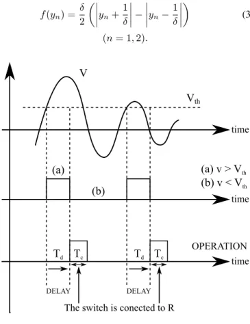
Furthermore, SW is the switch controlled by the amplitude, switch is connected to the resistor R in the case of amplitude is larger than the threshold, and connect time is represented by T
c. Also, this switching operation is included delay, and delay time is represented by T
d. Figure 2 shows the switching operation. Voltage reaches the threshold at a certain time, the
switch is not connected to the resistor immediately, which is connected for T
cseconds after T
dseconds. Namely, v
1nreaches V
th, two chaotic circuits coupled via resistor R is connected for T
cseconds after T
dseconds. Figure 3 shows the circuit realization. This circuit is consisted two Monostable Multivibrators. Monostable Multivibrator 1 outputs a pulse at regular intervals in reaction to the rising edge of the input pulse, and Monostable Multivibrator 2 outputs a pulse at reg- ular intervals in reaction to the falling edge of the input pulse.
Pulse width of Monostable Multivibrator 1 is corresponding to the delay time, and pulse width of Monostable Multivibrator 2 is corresponding to the connection time.
L
1L
2C -r
v
11i
11i
12v
dL
1L
2C -r
v
11i
11i
12v
dL
1L
2C -r
v
21i
21i
22v
dL
1L
2C -r
v
21i
21i
22v
dR DELAY(T
d)
SW
Fig. 1. Circuit model.
By using the variables such that
- 24 -
IEEE Workshop on Nonlinear Circuit Networks
December 13-14, 2013
i
n1=
√ C L
1V x
n, i
n2=
√ L
1C L
2V y
n, v
n1= V z
nα = r
√ C L
1, β = L
1L
2, δ = r
d√ L
1C L
2,
γ = 1 R
√ L
1C , t = √
L
1C
2τ, ” · ” = d dτ .
(1) That the equation (1) is normalized as
˙
x
n= αx
n+ z
n˙
y
n= z
n− f (y
n)
˙
z
1= − x
1− βy
n− γ(z
1− z
2)
˙
z
2= − x
2− βy
n+ γ(z
1− z
2)
(2)
(n = 1, 2),
The nonlinear function f (y
n) corresponds to the I − V characteristics of the nonlinear resistors consisting of the diodes and are assumed to be described as follows;
f (y
n) = δ 2
( y
n+ 1 δ
− y
n− 1
δ )
(3) (n = 1, 2).
V
thtime
time
time V
DELAY DELAY
The switch is conected to R (b)
(a) (a) v > V
th(b) v < V
thT
dT
dOPERATION
T
cT
cFig. 2. Switching operation.
III. S YNCHRONIZATION P HENOMENA
We investigate the phenomenon for the case of varying T
cin the circuit of Fig. 1.
L
1L
2C -r
v
11i
11i
12v
dL
1L
2C -r
v
11i
11i
12v
dL
1L
2C -r
v
21i
21i
22v
dL
1L
2C -r
v
21i
21i
22v
dR
V
th MonostableMultivibrator 1Monostable Multivibrator 2