九州大学学術情報リポジトリ
Kyushu University Institutional Repository
化学的または物理的手法により調製した金ナノ粒子 による正極/有機半導体界面修飾
王, 丹
https://doi.org/10.15017/1398546
出版情報:Kyushu University, 2013, 博士(工学), 課程博士 バージョン:
権利関係:Fulltext available.
Interfacial Modification at Anode/organic Semiconductor by Gold Nanoparticles Prepared
with Chemical or Physical Methods
Dan Wang
Department of Applied Science for Electronics and Materials, Interdisciplinary Graduate School of Engineering Sciences,
Kyushu University, Kasuga, Fukuoka 816-8580, Japan
2013
i
Abstract
The electrical contact between an anode and an adjacent organic semiconductor is one of the most fundamental issues in organic devices. Because of the closed shell structure of organic semiconductors, the contact is controlled by inserting modification layer at the interface to improve energy level alignment. However, the working mechanism of the modification for the carrier injection enhancement has not been understood yet. In this study, it has been revealed that gold nanoparticles with mean diameter 2-3 nm, which were synthesized either chemically or physically and placed sparsely on an anode can enhance the hole injection in hole-only devices dramatically and performances of both OLEDs and OSCs due to the electrical dipole based on the charge in the nanoparticles.
The hyper-branched polystyrene (HPS) stabilized gold nanoparticles (HPS-Au) were synthesized by chemical reduction. They were spun on indium tin oxide (ITO) electrode. The hole current density was a 1.5 orders of magnitude higher than the reference. This enhancement can be caused by just 1% surface coverage by HPS-Au.
The driving voltage of organic light emitting diode (OLED) can be reduced more than
1V by the HPS-Au insertion. The HPS-Au showed electrophoretic movement in organic
layer, indicating it is negatively charged. The electric dipole induced by the negative
ii
charge should cause the upward shift of vacuum level and reduction of the hole injection.
Gold nanoparticles were also prepared by physical methods. Vacuum deposited gold on ITO surface forms nanoparticles. A HPS layer was spun on ITO surface, followed by the gold deposition. The work function (WF) of the ITO was increased and the hole current was also enhanced by the evaporated gold nanoparticles. The WF change and current enhancement were more significant in the presence of the HPS under layer and with UV-ozone treatment than those in the absence of the layer or without UV-ozone treatment. The separation of the nanoparticle from the electrode should cause the more effective enhancement. When it was applied in OSCs as an anode buffer, the performance is also highly enhanced.
Arc plasma gun (APG) is another physical method to prepare Au nanoparticles.
The nanoparticles by APG can also increase the WF of ITO and enhance the hole current when the nanoparticles were treated by UV-ozone. Some chemical spices induced during the treatment would be the source of the negative charge on the nanoparticles. Comparing with evaporated nanoparticles, it can act as an hole injection layer without HPS under layer, therefore, the HPS is not essential for the hole injection.
The UV-ozone treatment would cause the negative charge on the nanoparticles to form
iii
the electric bilayer at the interface.
The gold nanoparticles are new class of surface modification materials to control
the contact between an anode and an organic semiconductor. Since the size and the
density can be manipulated easily, it would be a powerful tool for the investigation of
the contact.
iv
Table of Contents
Abstract ... i
Table of Contents ... iv
List of Figures ... vii
List of Tables ... x
Abbreviations ... xi
Chapter 1 Introduction ... 1
1.1 Organic semiconducting molecules and polymers ... 1
1.1.1 Basic concepts ... 1
1.1.2 Characteristics of organic semiconducting material and its application ... 2
1.2 Theory of metal/organic interface ... 3
1.2.1 Interface alignment theory—Mott-Schottky (MS) Model ... 4
1.2.2 Band bending in organic layer ... 5
1.2.3 Vacuum level shift and its effect on energy barrier at interface ... 6
1.2.4 Origins of interface dipole ... 8
1.3 Organic electronic devices ... 11
1.3.1 Organic light emitting diodes (OLEDs) ... 11
1.3.1.1 Basic knowledge ... 11
1.3.1.2 Structure and working principle ... 13
1.3.1.3 Hole injection layer ... 16
1.3.2 Organic Solar Cell ... 18
1.3.2.1 Structure and working principle ... 18
1.3.2.2 Device characterization ... 22
1.3.2.3 Anode buffer layer ... 25
v
1.4 Resent study on modification layer on ITO surface ... 26
1.4.1 Interfacial modification layer ... 26
1.4.2 Modification materials on ITO surface and Mechanism ... 27
1.4.3 Nanoparticles on modification layer... 31
1.5 Proposal of small size gold nanoparticles as modification layer ... 33
1.5.1 Introduction of HPS-Au ... 33
1.5.2 Research approach and Purpose of this work ... 34
1.6 References ... 37
Chapter 2 Effect of HPS-Au Nanoparticles on Hole Injection ... 42
2.1 Background ... 42
2.2 Experiment ... 42
2.3 Results and Discussion ... 47
2.3.1 Effect of HPS-Au on hole-only device ... 47
2.3.2 Mechanism Investigation ... 49
2.3.3 Effect of HPS-Au on OLEDs ... 59
2.4 Conclusion ... 63
2.5 References ... 65
Chapter 3 Effect of Evaporated Au on Hole Injection ... 66
3.1 Background ... 66
3.2 Experiment ... 67
3.3 Result and Discussion ... 70
3.4 Conclusion ... 79
3.5 References ... 81
Chapter 4 Effect of APG-Au Nanoparticles on Hole Injection ... 83
vi
4.1. Background ... 83
4.2. Experiment ... 83
4.3. Results and Discussion ... 86
4.4. Conclusion ... 100
4.5. References ... 101
Chapter 5 Conclusion ... 102
List of Publications and Presentations ... 106
Acknowledgement ... 107
vii
List of Figures
Fig. 1.1 Formation of energy barrier of metal/semiconductor interface (a) before
contact; (b) after contact ... 5
Fig. 1.2 Vacuum level alignment for metal/organic interfaces (a) without band bending; (b) with band bending ... 7
Fig. 1.3 Charge transfer across the interfaces (a) strong acceptor/low work unction metal; (b) strong donor/ high work function metal (or strong acceptor) ... 9
Fig. 1.4 interface dipole via modification of metal surface (a) before modification; (b) after modification ... 10
Fig. 1.5 interface dipole by chemical bond and polar molecule (a) chemical bond; (b) polar molecule ... 11
Fig. 1.6 The configuration and working mechanism of OLEDs (a) basic sandwiched structure; (b) conventional structure ... 15
Fig. 1.7 The configuration of dye-sensitized solar cell ... 21
Fig. 1.8 The structure of inverted OSC and tandem OSC (a) inverted structure; (b) tandem structure ... 22
Fig. 1.9 The scheme of OSC measurement system ... 23
Fig. 1.10 current density versus voltage characteristic ... 24
Fig. 1.11 The equivalent circuit of OSC ... 25
Fig.1.12 scheme of Step-wise energy level formation in OLED ... 28
Fig. 1.13 Energy level at interface with MoOx
57... 29
Fig. 1.14 Modified energy alignment by MoO
358... 30
Fig. 1.15 Schematic representation of HPS synthesis ... 34
viii
Fig. 1.16 Structure of conventional hole-only device ... 35
Fig. 2.1 The structure of hole-only device and OLED with HPS-Au modified ITO (a) hole-only device; (b) OLED... 43
Fig. 2.2 Schematic configuration of EL system ... 45
Fig. 2.3 Schematic diagram of AC-2 ... 46
Fig. 2.4 (a) the current density versus voltage characteristics of the HPS-Au hole-only device and (b) the comparison of the current density-voltage between the HPS-Au device (squre) and the reference device without Au (circle) ... 48
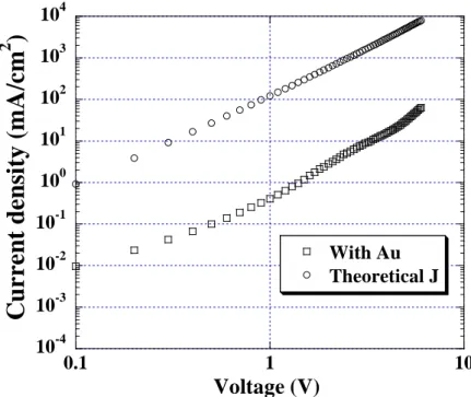
Fig. 2.5 current density comparison between the actual value (square) and theoretical value (circle) of HPS-Au hole-only device ... 50
Fig. 2.6 SEM image of ITO/HPS-Au ... 51
Fig. 2.7 XPS spectrum of (a) ITO/HPS-Au and (b) ITO/Evaporated Au ... 53
Fig. 2.8 TEM image of ITO/Evaporated Au ... 54
Fig. 2.9 (a) the scheme of the energy level alignment before voltage applied and (b) the effect of interface dipole on the energy level alignment after voltage being applied ... 56
Fig. 2.10 (a) Topography and (b) surface potential image of HPS-Au/Au (111) sample (c) Histogram of surface potential signals shown in (b). ... 56
Fig. 2.11 (a) SEM image of ITO surface treated with the HPS-Au solution at 3 times higher concentration (b) comparison between the different Au concentration ... 58
Fig. 2.12 The performance comparison between the OLEDs with (square) and
without HPS-Au (circle) (a) Current density-Voltage characteristic (b)
luminance-voltage characteristic ... 60
ix
Fig. 2.13 The EQE of the OLEDs with and without HPS-Au (a) device with
HPS-Au; (b) device without HPS-Au ... 61
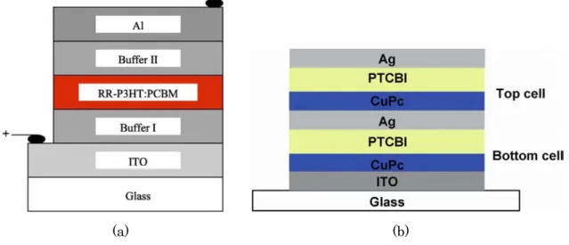
Fig. 2.14 Structure of OSCs ... 62
Fig. 2.15 Sculptures of P3HT and PCBM ... 62
Fig. 3.1 Schematic of XPS measurement ... 70
Fig. 3.2 TEM image of evaporated Au nanoparticles ... 71
Fig. 3.3 XPS of Si/HPS/e-AuNP before and after UV-ozone treatment ... 75
Fig. 3.4 J-V characteristics of HOD1(▲), HOD2(◊), HOD3(×) and HOD4(□) ... 77
Fig. 3.5 J-V property of device of ITO/e-Au NPs (1nm)/UV 40min/NPB/Al ... 78
Fig. 4.1 The schematic of work mechanism of arc plasma gun ... 85
Fig. 4.2 The polarization image of arc plasma gun ... 85
Fig. 4.3 TEM images of APG-Au with different pulses ... 88
Fig. 4.4 current density-voltage characteristics with UV-ozone treatment time dependence ... 93
Fig. 4.5 XPS spectra of HPS/APG-AuNPs at 3 pulses before and after UV-ozone treatment ... 94
Fig. 4.6 current density-voltage characteristics with different HPS thickness ... 96
Fig. 4.7 SEM image of 3-pulse APG-Au on ITO surface ... 98
Fig. 4.8 J-V characteristics of OSCs with the structure of ITO/X/P3HT:PCBM/
LiF/Al ... 99
x
List of Tables
Table 2.1 Device parameters of the three devices ... 63
Table 3.1 The work function of ITO modified by HPS and evaporated Au ... 73
Table 3.2 OSC performances of the ITO/buffer layer/P3HT:PCBM/LiF/Al ... 79
Table 4.1 WF of ITO with 10 pulses of APG ... 87
Table 4.2 The performance of devices with different modification layer ... 99
xi
Abbreviations
APG: arc plasma gun EF: Fermi level EML: emitting layer
EQE: external quantum efficiency FF: fill factor
HIL/EIL: hole/electron injection layer HOMO: highest occupies molecular orbits HOD: hole-only device
HPS: hyper-branched polystyrene
HTL/ETL: hole/electron transporting layer J: current density
Jsc: short circuit current density
LUMO: lowest unoccupied molecular orbits OFET: thin-film filed effect transistor OLEDs: organic light-emitting diodes OSCs: organic solar cells
PCE: power conversion efficiency
RFID: organic nano-radio frequency identification devices V: voltage
VL: vacuum level
Voc: open circuit voltage
WF: work function
1
Chapter 1 Introduction
1.1 Organic semiconducting molecules and polymers 1.1.1 Basic concepts
Organic semiconducting molecules and polymers are a kind of organic materials composed of π-conjugated bonds, an alternating single and double carbon-carbon bond, which is also called π-conjugated molecules and polymers. Usually, oxygen, nitrogen, and sulfur exist as building elements in materials. The hole or electron could move via π-electron could overlaps by hopping, tunneling and related mechanisms.
Based on frontier molecular orbital theory
1, LUMO which is simplified from
lowest unoccupied molecular orbital is an electron acceptor representing the ability to
obtain an electron, which performs like the minimum conduction band in inorganic
semiconductors; and HOMO being acronyms of highest occupied molecular orbital
represents the ability to donate an electron, which performs like the maximum valence
band. The value of energy gap between HOMO and LUMO is used to estimate the
ability of excitation of material. The larger of the value is, the more difficult to be
excited. This gap can be adjusted easily in many ways, such as, using different chemical
substituent on the backbone or different type of electron donating side-chains
2.
2
1.1.2 Characteristics of organic semiconducting material and its application
The organic semiconductor molecules are bonded with each via Van der Waals, which has advantages of easier being processed comparing with inorganic materials, good compatibility with a wide variety of substrates including flexible plastics, large size, low cost both in material synthesis and device fabrication, more flexible, and also biodegradable due to being made from carbon.
All of these advantages open the door for organic semiconductor to many exciting and advanced new applications that would be impossible using copper or silicon, such as displays based on organic light emitting diodes (OLED)
3, organic solar cell (OSC)
4, laser
5, thin-film filed effect transistor (OFET)
6, organic nano-radio frequency identification devices (RFID)
7, electrochemical transistors
8, and bio-sensing
9applications.
The contribution of change has been observed in the crystal structure with temperature to the variation of carrier mobility with temperature. With the temperature increasing, there will be slight increase in electron mobility along the crystal direction.
Conductive polymers always have high resistance; therefore, they are not good
conductors of electricity. Because of poor electronic behavior (lower mobility), they
have much smaller bandwidths. Also devices usually have shorter lifetimes and are
3
much more dependent on environment conditions than inorganic electronics. All of these challenges are needed to overcome to promote the widely commercial application of organic semiconductor.
1.2 Theory of metal/organic interface
The analysis of the status at metal/organic interface is a great issue for understanding and developing the working process of organic electronic devices.
Interface alignment between metal and organic interface determines charge injection and charge flow in devices.
Energy alignment at electrode/organic interface is not a simple combination of
energy level of bulk materials, due to the complex status of electron distribution on
metal surface; even more, when organic material deposited on metal surface,
redistribution or charge transferring also possibly happed, which is widely researched in
the surface science. When the metal is deposited on organic surface, the energy
alignment may be totally different with metal/organic interface. Here, only the case of
metal/organic interface is introduced.
4
1.2.1 Interface alignment theory—Mott-Schottky (MS) Model
Interface energetic is dependent on the sequence of the deposition, the electronic structures of the organic material and of the metal, and the metal/organic interaction.
Usually, when the organic layer is spin coated or evaporated on metal surface, there is no chemical interaction occurred
10.
Energy levels in organic semiconductor are filled by electrons following the Fermi statistics, so the concept of Fermi level is always valid in organic semiconductor.
Mott-Schottky (MS) model which is well-known for inorganic semiconductor/metal contact has been applied to organic/metal interface without any discussion until recently
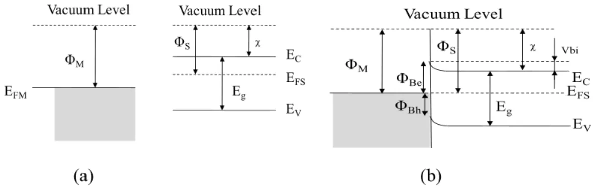
11. Before contact, the two surfaces are in their original state, which is shown in Fig. 1.1(a). The work function of the metal Φ
Mis equals to the distance of metal Fermi level E
Fto the vacuum level. The organic semiconductor has a conduction band level Ec (LUMO) at χ from the vacuum level V
L, where χ is the electron affinity. E
Vis the valence band level (HOMO) from vacuum level, which is equal to the ionization potentials (Φ
IP). And the band gap Eg is defined as the difference between the E
Vand E
C.
After contact, energy alignment as MS model which assumes vacuum level
alignment right at the interface region, band bending in the space charge layer (SCL) to
5
achieve the alignment of the bulk Fermi level between them is shown in Fig. 1.1(b). In this model, same Fermi level in the bulk organic layer as metal and thermal equilibrium state are thought to be achieved, therefore, Due to redistribution of charges, a layer with band bending with a built in potential V
biwill be formed. The interface energy barrier (Φ
B) refers to energy offset between the Fermi-level of the metal and the band edge or molecular orbital in the semiconductor (E
Cfor electrons and E
Vfor holes), which is shown in Fig. 1.1(b). And Φ
Befor electron can be expressed as |χ-Φ
M|, and for holes, Φ
Bh=|Φ
IP-Φ
M|=|χ+ Eg -Φ
M|.
(a) (b)
Fig. 1.1 Formation of energy barrier of metal/semiconductor interface (a) before contact; (b) after contact
1.2.2 Band bending in organic layer
However, lots of researches have demonstrated that Mott-Schottky model is too naive to explain metal/organic interface. First is about the happening of band bending in
E
FMVacuum Level
E
VVacuum Level
E
FSE
gΦ
S χΦ
ME
CVacuum Level
E
VE
FSE
gΦ
S χΦ
MΦ
BeΦ
BhE
CVbi
6
organic semiconductors and the achieving of Fermi level alignment. Because energy gap between HOMO and LUMO of organic semiconductor is very large, the organic semiconductor performs like an insulator in which the band bending is not considered.
Moreover, being different from inorganic semiconductors, organic materials are bound via van der Waals force; therefore, wave function and charge density are localized with each molecule, which indicates that carrier exchange will not be effective. So instead of band bending, energy level bending is more appropriate
12.
The case of band bending only happens when sufficient number of mobile charge carriers exists in material, either in a rather thick organic layer or organic layer with good semiconducting character. For the case of very thin layer of molecular material in UHV, the alignment of the Fermi level is not easily established
13.
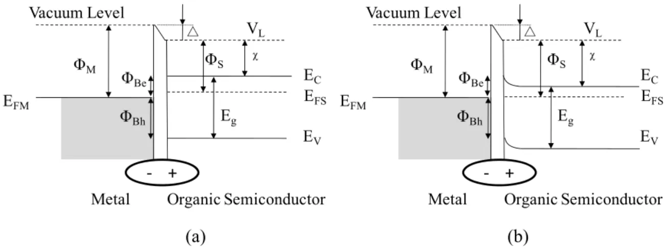
1.2.3 Vacuum level shift and its effect on energy barrier at interface
First, experiments from photoemission spectroscopy have revealed that vacuum level alignment does occur in most organic/metal interfaces due to the formation of an interface dipole inducing vacuum level shift △, which is shown in Fig. 1.2. Under this case, energy barrier for charge injection and V
biare both modified by △.
For a metal, the energy of vacuum level at infinite distance, VL(∞), is always
7
different from the energy of vacuum level at surface, VL(s), due to the surface dipole layer formed by the tailing of the electron cloud at the surface
14. When the surface of organic semiconductor is in the range of metal surface dipole, assuming no rearrangement of the electric charge happened; its energy levels will be the same with VL(s) in an extremely narrow distance from the surface. However, in realistic, because of various reasons, another interface dipole which is a different dipole from the mentioned above will be formed right at the interface, therefore, a shift △ of VL in the narrow distance from surface of organic semiconductor is formed, shown in Fig. 1.2 (a).
The case of band bending also happened is shown in the Fig. 1.2 (b).
(a) (b)
Fig. 1.2 Vacuum level alignment for metal/organic interfaces (a) without band bending;
(b) with band bending
With vacuum level shift, the injection energy barrier needs to be modified by △, which is expressed as Φ
Befor electron can be expressed as |χ-Φ
M|+△, and for holes,
Metal E
FMV
LE
VOrganic Semiconductor E
FSE
gΦ
S χΦ
MΦ
BeΦ
BhVacuum Level
E
C△
‐ +
Metal E
FMV
LE
VOrganic Semiconductor E
FSE
gΦ
S χΦ
MΦ
BeΦ
BhVacuum Level
E
C△
‐ +
8
Φ
Bh=|Φ
IP-Φ
M|=|χ+ Eg -Φ
M|-△, where △ is smaller than zero. So it can be seen that when the vacuum level is downward shifted, the injection barrier for hole injection becomes larger comparing that of without considering shift.
The trend of shift is determined by the interface dipole. An interface dipole with its negative pole at the side of metal and its positive pole at the side of organic semiconductor will make the vacuum level has a downward shift, then decrease the HOMO energy of the organic semiconductor. As a result, the energy barrier for hole is increased. In the opposite, the barrier will be decreased.
So it can be seen that when depositing organic layer on metal, if the shift of vacuum level happened, the energy alignment at interface will have obviously change, which will influence the energy barrier for charge movement. UPS is a widely used method to investigate the energy alignment at interface
15. A number of publications explain its principle and application in surface science and organic electronics.
1.2.4 Origins of interface dipole
Vacuum level shift is caused by an interface dipole the origins of which are still in
dispute. Here summarized some which are already accepted by researchers. This
interfacial dipole may be formed right at the interface due to various origins such as
9
charge transfer across the interface, redistribution of electron cloud, interfacial chemical reaction, and other types of rearrangement of electronic charge
16,17.
Charge transfer between the metal and the organic layer can be described as positive and negative charges separated across the interface. It is usually applied for the combinations of (strong acceptor) vs (low work function metal) shown in Fig. 1.3(a), combinations of (strong donor) vs (high work function metal), (strong donor) vs (strong acceptor)
18,19.
(a) (b)
Fig. 1.3 Charge transfer across the interfaces (a) strong acceptor/low work unction metal;
(b) strong donor/ high work function metal (or strong acceptor)
The second formation of interfacial dipole is caused by the image effect or the modification of the surface dipole at metal surface
20, or the rearrangement of the electron cloud at the metal surface
21. The tailing part of the electronic cloud into
⊖ ⊕ e
-⊖ ⊕ e
-organic metal metal organic
10
vacuum Fig. 1.4 (a) pushed back by repulsion with the electron cloud in the adsorbate, resulting in an effectively positive charging of the vacuum side by adsorption compared with the bare surface Fig. 1.4 (b).
(a) (b)
Fig. 1.4 interface dipole via modification of metal surface (a) before modification; (b) after modification
The third factor is other types of chemical interaction than charge transfer, leading to the rearrangement of the chemical bonds, or to the formation of new bonds
22, which is shown in Fig. 1.5 (a). The fourth possible reason is the nature of polar organic molecule as shown in Fig. 1.5 (b).
⊕ ⊖ ⊖ ⊕ ⊖
⊕ ⊖
Chemical bond
⊕ ⊖
metal Organic metal Organic
11
(a) (b)
Fig. 1.5 interface dipole by chemical bond and polar molecule (a) chemical bond; (b) polar molecule
1.3 Organic electronic devices
Besides surface science, organic electric devices such as organic light emitting diodes (OLEDs), organic solar cells (OSCs) are another field of application of interface investigation which provides direct evidence for the charge injection or extraction mechanism in these devices. Also the electronic structure at interface can help research to design and modify the structure of devices.
In OLEDs, charges need to be injected from electrode under the external electric field. Whereas, in OSCs, charges need to be extracted from organic layer to electrode, the direction of charge movement is opposite to OLEDs. Next, the fundamental knowledge and mechanism of OLEDs and OSCs will be introduced, respectively.
1.3.1 Organic light emitting diodes (OLEDs) 1.3.1.1 Basic knowledge
Organic light emitting diodes (OLEDs) is a kind of device which can be emitting
light through the combination of holes and electrons in heterojunction based on organic
12
semiconducting materials. Due to its high brightness at low voltage, broad spectrum, less power consumption, very thin thickness, it could be applied in the fields of general space illumination, large-area light-emitting elements, electronic paper, full color printing.
Since the electro luminance (EL) phenomenon was observed through single crystals of anthracene in 1960s
23,24, it was until mid-1980s that the first small molecular organic light emitting diode (OLED) with high efficiency and low driven voltage was successfully realized by Tang and VanSlyke
25through a sandwiched thin film structure deposited from organic small molecule. Then in 1990, the first device based on solution processed conjugated polymers was fabricated by Cambridge group
26. This conjugated polymer based device could overcome the long-term stability problem of vacuum-deposited film and also could bring higher quantum yields. The conjugated polymer electrode in flexible light-emitting diode
27on a ‘plastic’ substrate brought a new mile-stone not only for the form of OLEDs but also for the life style of human beings.
The research and development of OLEDs involves conceptual, experimental, and
structural challenges
28. The motivation for this renewed field can be briefly summarized
as the easy of production and low cost. The production of small molecule devices and
13
displays usually involves thermal evaporation in a vacuum. This makes preparing process more expensive and of limited use for large-area devices than other processing techniques. However, contrary to polymer-based devices, the vacuum deposition process enables the formation of well controlled, homogeneous films, and the construction of very complex multi-layer structures. The high flexibility in layer design, enabling distinct charge transport and charge blocking layers to be formed, is the main reason for the high efficiencies of the small molecule OLEDs.
1.3.1.2 Structure and working principle
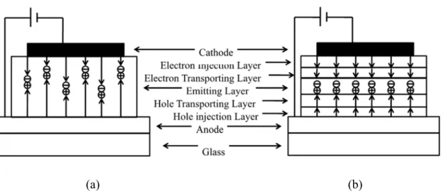
Fig. 1.6 (a) shows an OLED structure with single layer in which the emitting layer (EML) consisting of organic materials is sandwiched by an anode and cathode. When an external electric filed is applied, hole and electron are injected from anode and cathode into EML respectively, and then recombine in the EML to form hole-electron pair (neutral exciton), a bound state of the electron and hole. When the exciton is decayed to the ground state, the light will be generated and emitted from the EML.
During EL process, the amount of hole and electron charges in EML is one of the
key elements related to EL efficiency. To get higher charges injection from electrodes
and mobility in organic layers, injection and transporting layer are necessary, which is
shown in Fig. 1.6 (b). In Fig. 1.6(b), adjacent to electrode layer, electron and hole
14
injection layer (EIL/HIL) is applied to enhance carrier injection efficiency and transporting layer (HTL/ETL) is used to transport the carrier into EML effectively and also block the opposite charges. To get higher hole-electron pairs, not only the amount of each kind charge need to be efficient, it is also important that the hole current is well balanced with electron current in order to avoid ohmic losses. In some designed structures, an extra electron-blocking layer (EBL) between EML and HTL or hole-blocking layer (HBL) between EML and ETL (not shown in Fig. 1.6 (b)) is employed to confine the electrons and holes in EML. However, it can also lead to high charge densities at the interfaces, which causes undesirable decrease of lifetime.
Besides the above construction, researchers also developed top Emission
structure
29, transparent structure
30, tandem structure
31 , 32, structure with graded
heterojunction
33to enhance device performance and be suitable in real commercial
application.
15
(a) (b)
Fig. 1.6 The configuration and working mechanism of OLEDs (a) basic sandwiched structure; (b) conventional structure
As electrons and holes are fermions with half integer spin, formed exciton may either be in a singlet or a triplet state depending on how the spins of electron and hole have been combined. Statistically three triplet excitons will be formed for each singlet exciton. When the singlet exciton decays to ground state, the fluorescence can be emitted from EML, the frequency of which depends on the band gap of the emitting material. Just thermal energy could be generated when the triplet states decay.
External quantum efficiency (EQE, η
exe) is an important factor to evaluate device performance, which follows
34:
(1)
Where η
phis the light out-coupling efficiency the value of which is ~1/2n
2~20% for a
glass substrate with index of refraction n=1.5, η
intis internal quantum efficiency, γ is
16
the ratio of injected electrons and holes (the electron-hole charge-balance factor) which is equal to 1, η
exis the fraction of total excitons resulting in radiative transitions (0.25 for fluorescent materials, and 1 for phosphorescent materials), Φ
pis the intrinsic quantum efficiency for radiative decay (including both fluorescence and phosphorescence) which is 100% when all radiative exictons generate light. In fluorescent materials, only singlets radiatively decay, η
exeis limited to 5%. Using phosphorescent emitting material which can harvest both singlet and triplet exitions, η
execan approach as high as 20%.
1.3.1.3 Hole injection layer
Low driving voltage is always preferred in commercial OLEDs, which can enhance the device efficiency and lifetime. Research shows that driving voltage has close relation with mobility of organic materials and charge carrier injection. The former one is depended on the characteristic of material, and the latter one is up to the injection barrier height at electrode (anode or cathode)/organic interface
35,36.
If the energy barrier between anode/HTL is 0, then an ohmic contact will be
formed at the interface, which means that charge do not need to overcome any barrier to
be injected. Under this condition, the current is controlled by space charge. Under the
17
condition without ohmic contact, it is called injected limited
37. However, from the experimental point, for the theoretical calculated contact barrier of
b≤0.3eV, it is thought that the current is space charge limited and the contact is ohmic. If the
b>0.3eV, the current is thought to be injection limited
The electrical characteristic describes the relation between current density and applied voltage, which involves the mechanism of current density. When the charge is space charge controlled, it is called space charge limited current (SCLC). In this model, the value of current density can be expressed as:
J εμ (2) where ε is the dielectric constant, μ means the mobility of the organic layer. When that the current is injection-limited which means that the charges needs to overcome a barrier to be injected from electrode
38., which can be described by the models of trapped charge limited current (TCLC)
39, Fowler-Nordheim tunneling current (FNTC)
40and thermal emission current (TEC)
41.
To realize ohmic contact, besides adopting suitable metal and organic materials,
inserting an HIL also can assist to decrease the charge injection barrier, even can obtain
ohmic contact. The part of 1.4 will introduce the main materials used as hole injection
layer, and their mechanism.
18
1.3.2 Organic Solar Cell
Organic solar cell (OSC) is a type of devices consisting of molecular or polymeric organic compounds as active parts, which can absorb and convert sunlight to electricity.
This device has been studied since the late 1950s, and as the efficiency and reliability being increased, OSC is thought to be a promising power supply candidate of next generation.
1.3.2.1 Structure and working principle
The basis of OSC is that light absorption results in the formation of excitions, a bound electron hole pair in active layers. When the active layers absorb a photon, an excited state is created and confined to a molecule or a region of a polymer chain. The excited state can be regarded as an electron-hole pair bound together by electrostatic interactions. Light absorption is the first step to generate current. Then the created excitons are transported to the photo active interface by diffusion.
Due to the diffusion distance of an exciton is limited by the diffusion coefficient and exponential lifetime of exciton, so the efficiency is limited by the active material.
Next, exitons are broken up into free charges with the aid of additional input energy and
the electron will transport to an electron acceptor material from electron donor material
19
by effective fields. The effective fields are set up by creating a heterojunction between two dissimilar materials. It is necessary that the acceptor material has a conduction band edge that is lower than that of the absorber material. When the charges are collected on a transparent conductive oxide electrode (such as ITO) and a metal electrode, the electrical energy generation process is finished.
Single layer cells
The single layer cell is the first attempt to prepare all-organic solar cell by sandwiching an organic material between two electrodes. However, device property strongly depends on the nature of the electrodes. Moreover, the quantum efficiency and power conversion efficiency are both very low.
Bilayer organic solar cells
A double-layer structure of p-type (electron acceptor) and n-type (electron donor) organic semiconductors is introduced between two electrodes, so a local electric field is generated at the interface between the two layers. This local field must be strong enough to break up excitions. This kind of device has higher efficiency than the single layer cell.
In this device, thickness of the two layers should be in the same range as the exciton
diffusion length to make sure that most excitons to diffuse to the interface and then
break up. However, for polymer, only a small amount of excitons can achieve at the
20
interface, which is the main reason for the low efficiency.
C60 is a goold electron acceptor due to its high electron affinity. And perylene derivatives are also a group of organic molecules with high electron affinity, which are often used as electron acceptor.
Bulk Heterojunction organic solar cell
In this type of device, the two kinds of materials are blended together and then sandwiched between two electrodes. If the length scale of the blend is similar to the exciton diffusion length, excitons created in either materials can diffuse to the interface and then break up.
C60 and its derivatives are also used as electron acceptor in the dispersed heterojunction photovoltaic cells, for example, an OSC with the blend of MEH-PPV or P3HT and a methano-functionalized C60 derivative as the heterojunction.
Now polymer/polymer blends are also used in dispersed heterojunction OSCs, like a blend of CN-PPV and MEH-PPV, and a blend of P3HT and PCBM.
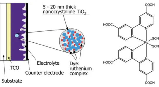
Dye sensitized photovoltaic cells are also considered as this type. In this type of
device, organic dye adsorbed at the surface of an inorganic wide-band gap
semiconductor is used for absorption of light and injection of the photoexcited electron
into the conduction band of semiconductor. So far, ruthenium dye-sensitized
21
nanocrystalline TiO
2solar cells reach an energy conversion efficiency of about 10%, the structure of which is shown in Fig. 1.7.
Fig. 1.7 The configuration of dye-sensitized solar cell
Graded Heterojunction organic solar cell
In this kind of device, the electron donor and acceptor materials are not only mixed together being similar with bulk heterojunction device, but also the gradient is gradual, which can overcome the disadvantage of short electron travel distance.
In addition, inverted OSC
42and tandem constructed OSC
43are also proposed to
enhance device performance, the structures of which are shown in Fig. 1.8 (a) and (b)
respectively.
22
(a) (b)
Fig. 1.8 The structure of inverted OSC and tandem OSC (a) inverted structure; (b) tandem structure
1.3.2.2 Device characterization
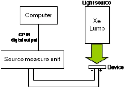
Fig. 1.9 indicates the OSC measurement system. Device is measured under
irradiation, and the characteristics that closely related to OSCs performance include
short circuit current density (Jsc), open circuit voltage (Voc), and incident
photon-to-current conversion efficiency (IPCE) and fill factor (FF).
23
Fig. 1.9 The scheme of OSC measurement system
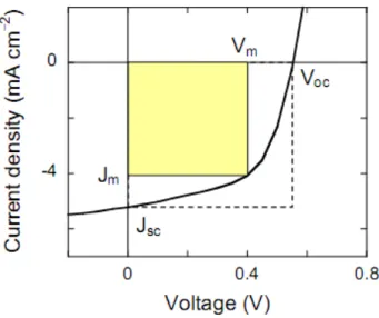
Jsc is the working current at the situation of short circuit, corresponding to no output voltage. While the Voc is the output voltage at status of open circuit, and the current is zero. The difference of work function between anode and electrode determines the value of V
oc.
FF is defined as the ratio of the maximum output power to the product of Voc and
Jsc, which is also the ratio between the two rectangles shown in Fig. 1.10.
24
Fig. 1.10 current density versus voltage characteristic
Fig. 1.11 shows an equivalent circuit of an OSC based on a single diode model
44. The output current in parallel with the junction can be described as follows:
I I I exp
∙1
∙(3) Where I
Lis the photo-current, I
0is the saturation current under reverse bias, R
shis the shunt current, R
sis series resistance, n is the ideality factor, q is the electronic charge, k is Boltzmann’s constant and T is the temperature in Kelvin.
When short circuit (V=0),
I I I exp
∙ ∙1
∙(4)
When open circuit (I=0),
25
I I I exp 1 (5)
Fig. 1.11 The equivalent circuit of OSC
So it can be seen that the values of R
sand R
shcan affect the V
ocand J
sc. The R
sis lower and R
shis higher, the device performance is better. Moreover, Rs and Rsh also influence the FF.
IPCE is defined as percentage of photons hitting the device's photo reactive surface that produce charge carriers, which can be indicated as following equation:
IPCE %
⁄⁄1240 ∙
⁄ ⁄(6)
1.3.2.3 Anode buffer layer
Same as OLEDs, when ITO is employed as anode in OSC, due to its high energy
26
barrier with adjacent donor layer or active layer, an anode buffer layer is often needed between anode and the active layer to facilitate extraction holes and the conversion efficiency could be increased dramatically by it. Low extraction efficiency could result in charge accumulation, thus induces poor device performance and also has negative influence on device lifetime.
In addition, if work function of ITO is increased by anode buffer, the hole can be extracted under the condition of open circuit so that larger V
occan be obtained. This is also introduced in 1.4 together with the hole injection layer in OLEDs.
1.4 Resent study on modification layer on ITO surface
1.4.1 Interfacial modification layer
Many functional interfacial materials have been developed, which can applied in
OLEDs or OSCs to optimize the property of metal/organic interface or organic/organic
interface. The functions of interfacial layer include: 1) minimizing the energy barrier for
charge injection or extraction; 2) determination of the relative polarity of devices; 3)
modification of the surface property to alter film morphology; 4) suppression of
diffusion and reaction between the electrode and polymer; 5) modulation of the optical
field as an optical spacer
45.
27
Here, the materials used as hole injection layer in OLEDs or anode buffer layer in OSC is called modification materials. Next the mechanisms and materials of modification layer at the interface of ITO/organic semiconductor to reduce energy barrier will be introduced.
1.4.2 Modification materials on ITO surface and Mechanism
ITO surface with appropriate treatment can possess a work function of 4.6-4.8eV.
However, this value still has a large energy barrier height with the HTL in OLED or active layer in OSC. Either the hole injection layer in OLEDs or the anode buffer layer in OSC, it can be called anode modification layer which plays important role in enhancing device efficiency. Here, some conventional employed materials and the related mechanisms are introduced.
Conducting organic materials with higher ionization potential such as
poly(3,4-ethylenedioxythiophene):poly(styrenesulfonate) (PEDOT:PSS)
46 , 47, cupper
phthalocyanine (CuPc)
48are the typical materials as hole injection layer and anode
buffer layer. Due to the ionization potential of these materials being between the work
function of anode and HOMO level of HTL, a stepwise energy level will be formed,
shown in Fig.1.12, which can dramatically decrease the energy barrier between
28
ITO/organic semiconductor layer, even the Ohmic contact can be formed when applied in polymer devices. The barrier that injected holes or extracted holes need to overcome will be much smaller comparing with the structure without hole injection layer.
However, some research shows that due to the acidic nature of PEDOT:PSS the ITO/PEDOT:PSS interface is not stable. Moreover the PEDOT:PSS layer is not a efficient electron-blocking layer because of its high leakage current.
Fig.1.12 scheme of Step-wise energy level formation in OLED
49Nano-composite in which nanoparticles are mixed with organic molecules like
PEDOT:PSS or doped in HTL is also a popular candidate as hole injection layer or
anode buffer layer. OLEDs with 6nm Ag nanoparticles in PEDOT:PSS as hole injection
layer in OLEDs can decreased the turn-on voltage
50. The blend of PEDOT:PSS and
29
inorganic nanoparticles like Ni was investigated as hole injection layer and the results shows that the doping of nanoparticles could induce performance to be increased
51.
N-type transition metal oxide like MoO
352,53, WO
354, V
2O
355is another series of materials widely using as anode interfacial layer. Kahn et.al. found these metal oxide could take large very deep electron affinity and ionization energy. It is thought that the enhanced hole injection from ITO is resulted from electron extraction from HOMO of HTL to the MoO
3conduction band, then the electron could attract hole injected from ITO surface
56as shown in Fig. 1.13. Some optimized device even can perform SCLC characteristic. As being employed in solar cell, the band bending at the interface leads to enhanced hole extraction which reduces series resistance
57, in which the modified interfacial energy alignment is shown in Fig. 1.14.
Fig. 1.13 Energy level at interface with MoOx
5630
Fig. 1.14 Modified energy alignment by MoO
357P-type metal oxide like NiO with a work fuction of 5.0 eV can also be used as anode modification layer which can form an Ohmic contact with HTL in OLED
58or active layer in OSC
59.
It is reported that a dense monolayer of small organic molecules, α-quarterthiophene-2-phosphonate (4TP) was bound to the ITO surface and then
p-doped with an electron acceptor, the work function of ITO was enhanced even more greatly than PEDOT:PSS
60. Another way to enhance hole injection is via p-doping of hole transporting layer with strong electron acceptor like (F4-TCNQ)
61, FeCl3
62, copper iodide
63and iodine
64.
A double hole injection layer consisting of Ag
2O/MoOx is also reported that it can
perform good hole injection ability, which is explained by the formation of a step wise
31
energy level
65and the injection process is with the help of Fowler-Nordheim (F-N) tunneling theory.
1.4.3 Nanoparticles on modification layer
Nanoparticles modifying anode surface is another effective way to enhance hole injection/extraction and make device performance obviously increase. Most widely utilizing is the surface plasmon coupled emission of gold or silver nanoparticles. With a 12nm chemically synthesized Au nanoparticles modified ITO surface, the fluorescence of OLED could be enhanced by 20 times
66. This result arises from that exciton energies are transferred into surface plasmon modes of the metal.
Plasmonic Au nanoparticles can also improve OSC performance due to its effect of redistribution of the optical field on light adsorption
67. Other nanoparticles like Ag, with surface plasmon characteristic also can be employed as anode modification layer both in OLEDs
68and OSC
69.
Due to localized surface plasmonic resonance, gold nanoparticles were also as insertion layer between ITO and PEDOT:PSS layer, which made power conversion efficiency of OSC increase
70.
A deoxyribonucleic acid (DNA) stabilized gold nanoparticles could be applied in
32
OLEDs as electron blocking layer, giving rise to higher luminance and current efficiency
71.
Numerous researches indicate that gold nanoparticles with size below 10nm on metal oxide can be surprisingly active for many reactions
72. It could be applied as catalysis for CO oxidation and propylene epoxidation, because CO and O
2can be physically absorbed on the Au surfaces. Under particular conditions, such as UV-ozone treatment, annealing, or plasma cleaning, the morphology and activity of gold can be changed
73, or chemically absorption can take place at gold surface
74.
Numerous researches indicate that gold nanoparticles with size below 10nm on metal oxide can be surprisingly active for many reactions
75. It could be applied as catalysis for CO oxidation and propylene epoxidation, because CO and O
2can be physically absorbed on the Au surfaces. Under particular conditions, such as UV-ozone treatment, annealing, or plasma cleaning, the morphology and activity of gold can be changed
76, or chemically absorption can take place at gold surface
77.
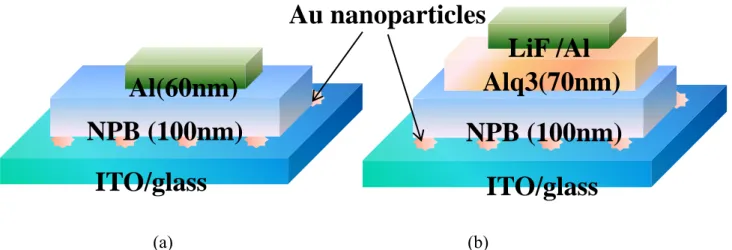
A 0.5-1nm thin evaporating gold layer presents small nanoparticles dispersing
substrate. There are also reports that insertion of a thin layer of gold between anode
substrate and organic layer in OSCs can highly enhance device performances
78,79,80.
However, the morphology of gold on substrate and the mechanism is not discussed in
33
detail.
1.5 Proposal of small size gold nanoparticles as modification layer
1.5.1 Introduction of HPS-Au
So far, small nanoparticles with size under 5nm are rarely used as modification layer. Hyper-branched polystyrene (HPS) with significant numbers of dithiocarbamate (DC) groups is a globular polymer soluble in most common organic solvents with diameter of 5 nm and can be insolubilized through thermal and photo-irradiation treatment due to cross-linking reaction, the process of which synthesis is shown in
Fig. 1.15. Utilizing the interaction between the DC group and gold, a kind of gold nanoparticles stabilized by hyper branched polymer (HPS-Au) with 2nm possessing negative charges
81was synthesized.
This HPS-Au nanoparticles has successfully been applied in organic electrical
bistable device (OBD)
81and organic photovoltaic (OPV)
82. Both devices have great
enhancement in properties comparing with reference devices.
34
S NEt2
S
H2C S NEt2
S
S S Et2N
S
S NEt2
S-DC
S
S S
S S Et2N
NEt2 S
NEt2
S
S NEt2
hν THF or toluene 20~30℃
S S S NEt2
S
NEt2
S
S Et2N
S
NEt2
S
S NEt2
S SSNEt2 S
Et2N S
CD DC
CD DC
DC
DC DC DC
CD DC CD
DC DC CD DC CD DC
Fig. 1.15 Schematic representation of HPS synthesis
1.5.2 Research approach and Purpose of this work
Single charge device is a kind of device in which only hole or electron exists due to
the counter carrier cannot be transformed through the device, which is utilized to
investigate the electric property of hole or electron, then further research the
corresponding mechanism. Qiao et.al. , used single carrier device to investigate the hole
and electron transporting characteristics in a o-CzOXD bipolar transporting layer to
controlling the charge balance. Murata
54utilized a hole-only device consisting of
35
ITO/MnOx/NPB/MnOx/Al to research the relationship between current and electric field.
Fig. 1.16 shows the structure of a conventional hole-only device. NPB as a HTL is sandwiched between anode of ITO and cathode of Al. Under the applied electric field, the hole is injected to NPB, and no electron exists due to the high energy barrier between NPB and Al.
Fig. 1.16 Structure of conventional hole-only device
In this work, negatively charged gold nanoparticles on anode modification is proposed to investigate its effect on hole injection in hole only device and in OLEDs, and OSCs, respectively.
Hole only device with structure in Fig. 1.16 is employed to study the effect of gold nanoparticles on hole injection, then discuss the mechanism of the effect based on interface science to find new useful direction in the application of nanoparticles in
ITO/glass NPB (100nm)
Al(60nm)
36
organic electronics.
This idea is also extended to the application of other chemically or physically
processed gold nanoparticles with comparative size in devices.
37
1.6 References
1 K. Fukui, T. Yonezawa, H. Shingu. The J. of Chem. Phys., 20 (4), 722 (1952).
2 A. Kraft, A. C. Grimsdale, and A. B. Holmes. Angew. Chem. Int. Ed., 37, 402(1998).
3 K. T. Kamtekar, A. P. Monkman, A. P. M. R. Bryce. Adv. Mater., 22 (5), 572 (2010).
4 H. Hoppe, N. S. Sariciftc. J. Mater. Res., 19 (7), 1924 (2004).
5 I. D. W. Samuel, G. A. Turnbull. Chem. Rev., 207, 1272 (2007).
6 H. Koezuka, A. Tsumura, T. Ando. Synthetic Metal, 18, 699 (1987).
7 V. Subramanian. Prof. of the IEEE, 93 (7), (2005).
8 D. Khodagholy, J. Rivnay, M. Sessolo, M. Gurfinkel, P. Leleux, L. H. Jimison, E.
Stavrinidou, T. Herve, S. Sanaur, R. M. Owen, and G. Malliaras. Nature Communication, 4, 2133 (2013).
9 J. T. Mabeck, G. G. Malliaras. Anal Bioanal Chem., 384, 343 (2006).
10 W. R. Salaneck, M. Logdlund, M. Fahlman, G. Greczynski, and T. Kugler. Materials Science & Engineering R-Reports, 34(3), 121 (2001).
11