首都大学東京 博士(理学)学位論文(課程博士)
論 文 名
層状カルコゲナイドからなる
2
次元ヘテロ構造の合成と物性著 者 小林 佑
審査担当者
主 査 宮田 耕充 准教授 委 員 真庭 豊 教授 委 員 柳 和宏 教授 委 員
上記の論文を合格と判定する
年 月 日
首都大学東京大学院理工学研究科教授会 研究科長
DISSERTATION FOR A DEGREE OF DOCTOR OF PHILOSOPHY IN SCIENCE
TOKYO METROPOLITAN UNIVERSITY
TITLE
:Synthesis and Physical Properties of Two-Dimensional Heterostructures Based on Layered Chalcogenides
AUTHOR
:Yu Kobayashi
EXAMINED BY
Examiner in chief:Assoc. Prof. Yasumitsu Miyata
Examiner
:Prof. Yutaka Maniwa
Examiner:Prof. Kazuhiro Yanagi
Examiner
QUALIFIED BY THE GRADUATE SCHOOL OF SCIENCE AND ENGINEERING
TOKYO METROPOLITAN UNIVERSITY
Dean
Date
Synthesis and Physical Properties of Two-Dimensional Heterostructures Based on Layered Chalcogenides
層状カルコゲナイドからなる
2
次元ヘテロ構造の合成と物性Yu Kobayashi
小林 佑Department of Physics, Graduate School of Science and Engineering, Tokyo Metropolitan University
2018
i
Contents
Chapter 1
Introduction to Transition Metal Dichalcogenides
1.1 Basic properties ... 1
1.1.1 Geometrical structures ... 1
1.1.2 Electronic structures ... 2
1.1.3 Optical properties ... 5
1.1.4 Electronic transport properties ... 6
1.2 Synthesis ... 8
1.2.1 Mechanical exfoliation ... 8
1.2.2 Chemical vapor deposition ... 9
1.3 Heterostructures ... 10
1.3.1 Band diagrams around semiconductor heterointerfaces ... 11
1.3.2 TMDC-based semiconductor heterostructures ... 13
1.4 Purposes ... 15
Chapter 2 Characterization Methods 2.1 Photoluminescence spectroscopy ... 17
2.2 Raman spectroscopy ... 20
2.3 Scanning tunneling microscopy and spectroscopy ... 22
ii
Chapter 3
Growth and Optical Properties of High-Quality Monolayer WS
2on Graphite
3.1 Introduction ... 25
3.2 Experimental methods... 26
3.3 Results and Discussions ... 28
3.3.1 Synthesis and crystal orientation of WS
2grown on graphite ... 28
3.3.2 Substrate-dependent optical properties of WS
2... 30
3.3.3 Temperature-dependent optical properties of WS
2... 38
3.3.4 Origin of multiple peaks appeared at low temperature or under vacuum for the WS
2on hBN and SiO
2/Si ... 41
3.4 Conclusions ... 42
Chapter 4 Slidable Atomic Layers in van der Waals Heterostructures 4.1 Introduction ... 43
4.2 Experimental methods... 44
4.3 Results and discussions ... 45
4.3.1 Demonstration of sliding atomic layers on van der Waals substrate surface45 4.3.2 Fabrication of in-plane and vertical contacts ... 46
4.3.3 Tearing and suspending of WS
2by sliding process ... 47
4.3.4 Origin of sliding process ... 50
4.4 Conclusions ... 51
iii
Chapter 5
Bandgap-Tunable Lateral & Vertical Heterostructures Based on Monolayer Mo
1-xW
xS
2Alloys
5.1 Introduction ... 52
5.2 Experimental methods... 54
5.3 Results and Discussions ... 56
5.3.1 High-temperature growth of Mo
1-xW
xS
2alloys ... 56
5.3.2 Uniformity of optical properties of Mo
1-xW
xS
2alloys ... 58
5.3.3 Low-temperature growth of Mo
1-xW
xS
2in-plane heterostructures ... 60
5.3.4 Low-temperature growth of Mo
1-xW
xS
2vertical heterostructures ... 61
5.3.5 Air stability of Mo
1-xW
xS
2alloys ... 65
5.3.6 STM observations of Mo
1-xW
xS
2based heterostructures ... 71
5.3.7 Spatial variation in the band structure of WS
2/Mo
1-xW
xS
2heterojunction . 73 5.4 Conclusions ... 75
Chapter 6 Modulation of Electrical Potential and Conductivity in an Atomic-Layer Semiconductor Heterojunction 6.1 Introduction ... 76
6.2 Experimental methods... 77
6.3 Results and discussions ... 79
6.3.1 Growth and structure models of TMDC-heterostructures ... 79
6.3.2 Characterization of monolayer heterostructures based on WS
2and MoS
2. 80 6.3.3 Characterization of bilayer heterostructures based on WS
2and MoS
2... 84
6.3.4 Observations of local electronic states of bilayer heterostructure interface 88 6.3.5 Origin of electronic potential modulation in bilayer hetero-structures ... 90
6.4 Conclusions ... 92
iv
Chapter 7
Alkali Metal-Assisted Growth in Metal-Organic Chemical Vapor Deposition of Two-Dimensional Layered Chalcogenides
7.1 Introduction ... 93
7.2 Experimental methods... 94
7.3 Results and discussions ... 95
7.3.1 Promoter-dependent growth of TMDC monolayers ... 95
7.3.2 Substrate-dependent growth of TMDC monolayers ... 99
7.3.3 Effects of promotors for MOCVD growth ... 100
7.3.4 Discussions of a roll of promotors for MOCVD growth ... 104
7.4 Conclusions ... 104
Chapter 8 Continuous Heteroepitaxy of Two-Dimensional Heterostructures Based on Layered Chalcogenides 8.1 Introduction ... 105
8.2 Experimental methods... 107
8.3 Results and discussions ... 109
8.3.1 Growth and characterization of TMDC monolayers ... 109
8.3.2 Heteroepitaxial growth of in-plane and vertical heterostructures ... 112
8.3.3 Atomic structures and electronic properties of heterointerfaces ... 118
8.4 Conclusions ... 121
v
Chapter 9
Conclusions ... 122
Acknowledgements ... 123
List of Publications ... 125
Bibliography ... 130
1
Chapter 1:
Introduction to Transition Metal Dichalcogenides
1.1 Basic properties
Transition metal dichalcogenides (TMDCs) are similar to typical two- dimensional (2D) materials such as graphene and hexagonal boron nitride (hBN). Graphene is a zero- bandgap semiconductor with a high carrier mobility of 2 × 10
5cm
2/Vs at room temperature[
1], while hBN is an insulator with a 6.1 eV bandgap[
2]. In contrast, TMDCs can exhibit various electronic states ranging from metallic to semiconducting, with band gaps of 1
to 3 eV, based on variations in their composition, crystal structure, and layer number[
3].
Thus, TMDCs have attracted significant attention with regard to applications as thin-film semiconductors. In this chapter, we introduce the basic properties of the TMDCs consisting of Group 6 transition metals that are used for this study.
1.1.1 Geometrical structures
The chemical formula of a TMDC can be summarized as MX
2, where M is a transition metal and X is a chalcogen[
3]. The structures in these materials are composed of three atomic layers: a single transition metal layer sandwiched between two chalcogen layers.
The atoms within each layer are connected by covalent bonding, whereas the layers are bound to one another via relatively weak van der Waals forces. In contrast to graphite,
Figure 1.1 Illustrations of typical two-dimensional materials.
2
bulk TMDCs display various stacking polytypes and polymorphs because the MX
2monolayers, which include three layers of atoms (X-M-X), can exist in either one of two phases. The most common polytypes are 1T, 2H and 3R, where the letters indicate trigonal, hexagonal and rhombohedral geometries, respectively, and the digits represent the number of X-M-X groups in the unit cell. The particular polytype of a TMDC will determined its physical properties.
1.1.2 Electronic structures
When discussing the electronic states of TMDC monolayers, it is helpful to employ the effective Hamiltonian for each compound. A previous theoretical analysis [
4] has shown that the Schrödinger equation for a MoS
2monolayer (as well as for other group VI dichalcogenides) is
(
𝛥
2 𝛾(𝑘
𝑥− 𝑖𝑘
𝑦) 𝛾(𝑘
𝑥+ 𝑖𝑘
𝑦) − 𝛥
2
) ( 𝜙
𝑐𝜙
𝑣) = 𝐸 ( 𝜙
𝑐𝜙
𝑣),
(𝛥 and 𝛾 are energy gap and proportional constant, respectively.)
where the value of (E) is
𝐸 = √𝛾
2𝑘
2+
𝛥24
.
From the above, it is evident that as 𝛥 → 0, 𝐸 = 𝛾𝑘. This represents a linear dispersion
of E, and 𝐸 = 𝛾𝑘 is, in fact, the dispersion relationship for graphene. The above equation
for E is graphed in Figure 1.2.
3
Figure 1.2 Graph of the TMDC energy band around the K (K’) point.
This graph demonstrates that TMDCs will have Dirac particles with mass, in contrast to graphene for which the Dirac particles are massless.
It is also possible to calculate the Hamiltonian for the spin-orbit interaction, which can be written as
ℋ
𝑆𝑂=
ℏ4𝑚2𝑐2 1 𝑟
𝑑𝑉 𝑑𝑟
𝑳 ⋅ 𝑺,
= 𝜉 𝑳 ⋅ 𝑺,
= 𝜉 (𝐿
𝑧𝑆
𝑧+ 𝐿
+𝑆
−+ 𝐿
−𝑆
+),
where L is the orbital angular momentum and S is the spin angular momentum. Based on
|𝑐⟩ and |𝑣⟩ , the Hamiltonian can be written as
ℋ ̂ = [
𝑆𝑂0 0 0 𝜆𝑆
𝑧],
indicating that only the electronic state of the valence band is affected by the spin-orbit interaction, and that the valence band is split.
From these results, the Hamiltonian matrix for the spin-orbit interaction around the K (K')
point is
4
ℋ ̂ = [
𝛥
2
𝛾(𝑘
𝑥− 𝑖𝑘
𝑦) 𝛾(𝑘
𝑥+ 𝑖𝑘
𝑦) −
𝛥2
+ 𝜆𝑆
𝑧] .
A simple graph of the energy dispersion relationship for the spin-orbit interaction is presented in Figure 1.3.
Figure 1.3 Graph of the TMDC energy band around the K (K’) point for a spin-orbit interaction.
This large spin-orbit interaction and broken inversion symmetry result in 150 meV splitting of the valence band of the MoS
2monolayer[
4-6], which exceeds the room temperature value of approximately 26 meV. Therefore, the K (K') point for the valence band maximum is occupied solely by down-spin (up-spin) electrons. As a result, TMDC monolayers will naturally possess spin-polarized states even in the absence of an external magnetic field, resulting in the coupling of spin and valley degrees of freedom.
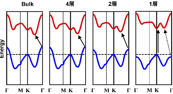
The electronic states of TMDC semiconductors are different between the bulk material
and monolayers. Figure 1.4 shows the energy band dispersions of bulk, 4L, 2L and 1L
MoS
2as determined by first-principles calculations[
3, 7]. In the case of bulk MoS
2, the
conduction band minimum is situated between the K and Γ points, while the valence band
maximum is located at the Γ point. As a result, bulk MoS
2is an indirect transition
semiconductor with an energy gap corresponded to a different range of wavenumbers. In
contrast, a MoS
2monolayer is a direct transition semiconductor because both the
conduction band minimum and valence band maximum are situated at the K point.
5
Consequently, this material will also be optically active.
Figure 1.4 Schematic illustrations of the energy band dispersions of bulk, 4L, 3L, 2L and 1L MoS2.
1.1.3 Optical properties
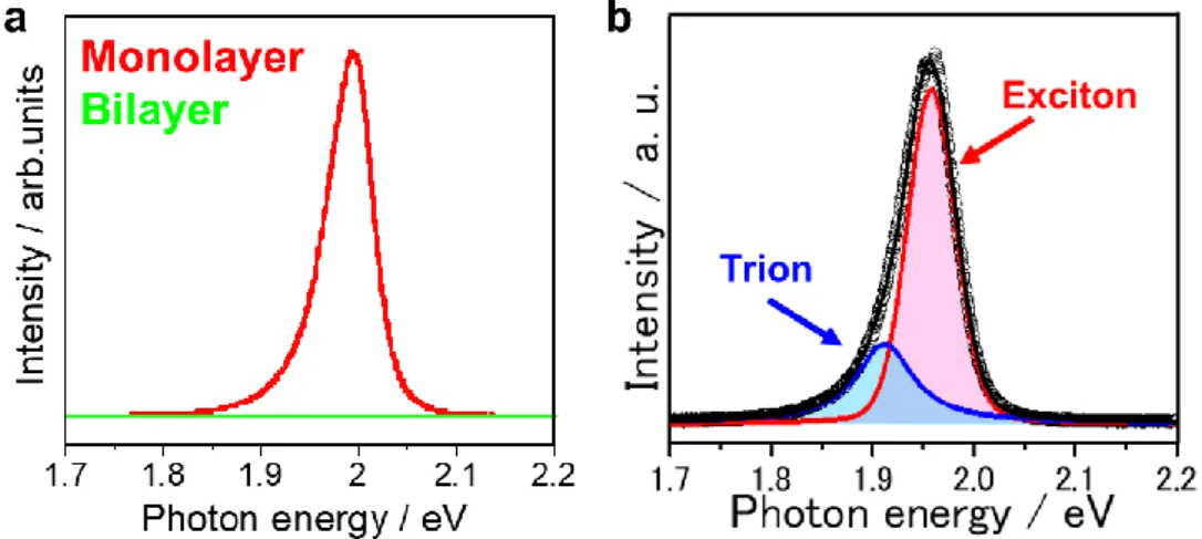
The optical properties of TMDC semiconductors can be tuned by modifying their electronic structures. Figure 1.5a presents the photoluminescence (PL) spectra of monolayer and bilayer WS
2, which demonstrate that the monolayer compound generated much more intense PL. The emission quantum yields change significantly depending on the number of layers, and are greatly increased in the case of a monolayer[
8].
The optical properties of TMDCs are dominated by electron and hole pairs known as
excitons. When a negatively charged electron and a positively charged hole are generated
in a semiconductor, they are typically attracted to one another by the Coulomb force and
enter a bound state, which is the exciton. In the case of TMDC monolayers, electrons and
holes are confined to a thin region of only a few atomic layers, such that stable excitons
are generated as a result of the intense quantum confinement effect[
3, 6]. Excitons in such
monolayers are therefore stable, since they have binding energy values of several 100
meV[
6], which are significantly greater than the room temperature thermal energy value
6
of approximately 26 meV.
A hole or electron can also bind to an exciton in a stable manner at room temperature, to form a charged exciton known as a trion. This phenomenon results in dramatically different characteristics than those displayed by conventional low-dimensional semiconductors. Figure 1.5b shows the PL spectrum of a WS
2monolayer grown on a SiO
2/Si substrate. The PL peak in this spectrum has two components, which correspond to the exciton and negative trion recombination peaks[
6, 9-10]. The binding energy of a trion is approximately 40 meV greater than that of an exciton[
6, 10-11]. Negative trions are observed in crystals grown on SiO
2/Si as a result of electron-doping due to the presence of charged impurities and structural defects. The full-width at half-maximum (FWHM) of the trion PL peak is 55 meV, and this relatively large value is attributed to inhomogeneous lattice strain caused by the substrate and/or structural defects. These low sample qualities are important in terms of defining the basic physical properties and applications of such materials.
Figure 1.5 (a) PL spectra of monolayer and bilayer WS2. (b) PL spectrum of a WS2 monolayer grown on SiO2/Si.
1.1.4 Electronic transport properties
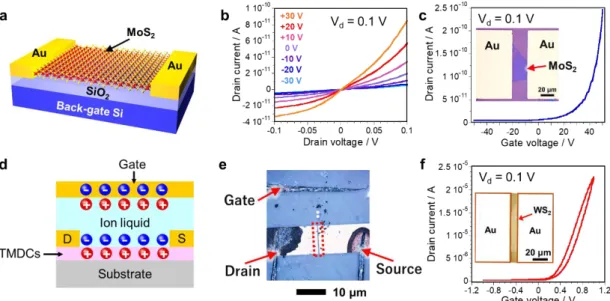
Semiconductor TMDCs exhibit certain characteristics that could be useful in field effect
transistors (FETs), including a lack of dangling bonds, structural stability, and high carrier
mobility comparable to that of Si. In 2011, Radisavljevic et al. demonstrated the high
7
carrier mobility of a MoS
2monolayer exfoliated from a bulk crystal, and fabricated a high on-off ratio transistor, as same as Figs. 1.6a-c [
12]. Although the mobility value reported by Radisavljevic is not exact because the capacitance of the device was incorrectly estimated, this report has prompted research regarding the electronics applications of MoS
2.
Recently, an electric double layer transistor (EDLT) in which the gate material is replaced with an electrolyte (Figure 1.6c) has attracted much attention[
13-16]. The capacitor gap in this device is approximately 1 nm and the resulting capacitance is approximately three orders of magnitude greater than that of a conventional insulator.
Using an oxide insulating film, the carrier density of the semiconductor can be controlled within the range of 10
12to 10
13cm
-2, although the carrier density in the EDLT can exceed 10
14cm
-2based on the application of a small gate voltage. Huang et al. reported the transfer characteristics of a WSe
2monolayer grown by the chemical vapor deposition (CVD) method[
13]. This EDLT incorporates an ion gel composed of the ionic liquid 1- ethyl-3-methylimidazolium bis(trifluoromethylsulfonyl)imide ([EMIM][TFSI]) as the electrolyte and poly(styrene-block-methyl methacrylate-block-styrene (PS-PMMA-PS).
This transistor was found to have a low driving voltage of 3 V or less, along with polarity control and a high on/off ratio of 10
6. The hole mobility in the device was approximately 90 cm
2/Vs. Similar results have been reported using MoS
2, MoSe
2and WS
2. The maximum electron mobility of MoS
2reached 60 cm
2/Vs, while that of WSe
2exceeded 100 cm
2/Vs. Thus, these results demonstrate that the EDLT concept is a useful means of tuning transistor characteristics. Figures 1.6e and f show the optical image and the transport properties of monolayer WS
2EDLT. This WS
2device exhibit n-type semiconductor behavior.
Furthermore, by taking advantage of the significant controllability of the carrier density, an EDLT can be used to modify other physical properties. A high-density carrier injection induced a superconducting phase in this material as a result of the field effect[
17-18].
Control of the thermoelectric properties of such devices has also been reported[
19].
TMDCs have been proposed for applications in flexible electronics because of their two-
dimensionality and excellent mechanical strength. Based on the optical characteristics
described above, TMDCs are also anticipated to have uses in simple transistors and in
8
optoelectronics such as photodiodes and light emitting diodes.
Figure 1.6 (a) Schematic illustration and (b, c) the room-temperature transfer characteristics of a back-gate FET based on a MoS2 monolayer. (d) Schematic illustration of the EDLT. (e) Optical image of EDLT device of monolayer WS2 grown on sapphire. (f) The room-temperature transfer characteristics of EDLT based on a monolayer WS2.
1.2 Synthesis
Two primary methods are used to synthesize TMDC monolayers: mechanical exfoliation and CVD, both of which are described below.
1.2.1 Mechanical exfoliation
Mechanical exfoliation involves peeling layers from a bulk TMDC crystal using adhesive
tape (Figures 1.7a and b) [
20-22]. The bulk TMDC crystals are typically synthesized using
chemical vapor transport[
23]. In the bulk crystals, the stacked monolayers are held
together solely by van der Waals forces, and so exfoliation proceeds readily. Novoselov
et al. obtained graphene monolayers from highly oriented pyrolytic graphite using this
same technique[
24-25]
.This method allows the facile production of TMDC monolayers but
shows poor reproducibility. In addition, it is difficult to peel off a single layer over a wide
area and so this technique is generally unsuitable for large-scale synthesis (Figure 1.7c).
9
Figure 1.7 Photographs of (a) a bulk WS2 crystal and (b) mechanical exfoliation of the WS2
using adhesive tape. (c) Optical microscopy image of a WS2 monolayer and multilayer fabricated by exfoliation on a SiO2/Si substrate.
1.2.2 Chemical vapor deposition
CVD is a popular means of synthesizing graphene, and CVD using Cu foil as a growth substrate allows wide graphene specimens to be fabricated [
26-28]. In this technique, a chemical reaction proceeds on the substrate surface or in the gas phase to form thin films.
This allowed the synthesis of films having large surface areas with well-controlled layer quantities on the substrates in the work reported herein. Interestingly, a wider range of substrates may be employed in the CVD synthesis of TMDCs. In the case of graphene, a metallic substrate has a catalytic effect, and it is necessary to consider other factors such as carbon and hydrogen solubility in the substrate[
28]. However, because the substrate will not show a catalytic effect during TMDC synthesis, any material that can withstand the synthesis temperature can be used. Choosing the correct substrate is important in the synthesis of 2D materials, as roughness, impurities, dangling bonds and other factors associated with the substrate can greatly affect the quality of the resulting material [
29-31].
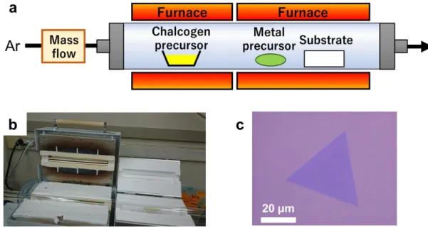
In preparation for TMDC synthesis using a typical CVD process, the substrate (such as
SiO
2/Si or sapphire) is initially cleaned using ethanol and/or an oxygen plasma. The clean
substrate is subsequently placed in a quartz tube that acts as a growth chamber and
precursor reagents are situated upstream of the substrate. The quartz tube is then heated
to 500 – 900 °C by a furnace, under an inert atmosphere. After the reaction, the quartz
tube is cooled to room temperature and the substrates is removed.
10
Figure 1.8 (a) Schematic illustration of the CVD apparatus, (b) a photograph of the CVD growth equipment, and (c) an optical microscopy image of WS2 grown on a SiO2/Si substrate via CVD.
1.3 Heterostructures
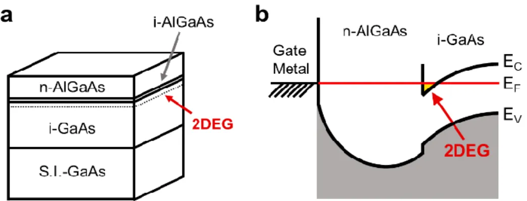
Semiconductors have been employed in light emitting and electronic devices, including semiconductor lasers and high electron mobility transistors. In these applications, the heterointerfaces in the semiconductor are one of the most important factors. In addition, the formation of a 2D electron gas (2DEG) is vital to the functioning of such heterostructures. In a 2DEG, electrons are two-dimensionally distributed throughout the semiconductor, and this gas is used to create inversion layers in metal-oxide- semiconductor field effect transistors and channels in high electron mobility transistors.
Figure 1.9 shows a structural model and an energy diagram for a heterostructure
composed of i-GaAs and n-AlGaAs. Here, the approximately 10 nm i-AlGaAs layer acts
as a spacer between the n-AlGaAs and i-GaAs. The confining potential around the
heterointerface resulting from band alignment and bending confines electrons two-
dimensionally. In this section, we focus on the band structure near the heterointerface in
TMDC heterostructures.
11
Figure 1.9 (a) Structural model and (b) energy diagram of a heterostructure composed of i- GaAs and n-AlGaAs.
1.3.1 Band diagrams around semiconductor heterointerfaces
Semiconductor heterostructures composed of combinations of different semiconductors are vital in applications such as light emitting and electronic devices. These structures are different from p-n (homo) junctions, in that discontinuities exist in the conduction and valence bands. In addition, heterostructures show different energy gaps and dielectric constants.
Band alignments
Band alignment (also referred to as natural band lineup) is a key factor determining the
characteristics of a heterostructure, because it reflects the relative positional relationship
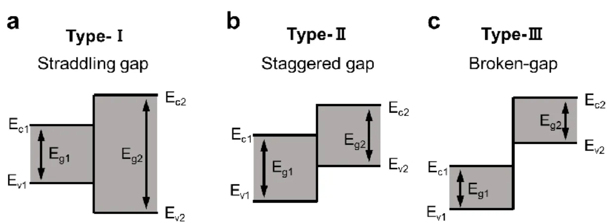
of the bands in the heterostructures. As shown in Figure 1.10, there are three types of band
alignments in semiconductor heterostructures. In type I heterostructures, one band gap is
situated within the other (Figure 1.10a), while types II and Ⅲ are associated with
staggered and broken-gap band alignments (Figures 1.10b and c). In a type I
heterostructure, electrons and holes are confined in the same layer and so the interaction
between the conduction and valence bands is important. In contrast, in type II and III
structures, which are typified by the presence or absence of an overlap between the
conduction and valence bands of adjacent layers, electrons and holes are separately
confined in adjacent layers. As such, the interaction between the conduction and valence
bands is important.
12
Figure 1.10 Schematic illustrations of band structures of (a) type I, (b) type II, and (c) type III semiconductor heterostructures.
Band bending
Band bending, which results from the formation of a heterostructure, is an important phenomenon. Figure 1.11 presents energy diagrams before and after heterostructure formation. Because the valence and conduction bands bend due to the curvature of the vacuum level, band discontinuities such as spikes and notches appear at the heterostructure interface. Such discontinuities are important characteristics of heterostructures. As an example, because a notch in a conduction band at an interface will have a lower energy level than other parts and potential barrier, electrons can be confined at a very high concentration by controlling the Fermi level.
Additionally, modulation of band structures can occur as a result of interface states formed by defects, dangling bonds, lattice strain and fixed charges (Figure 1.12). Interface states formed by defects, dangling-bond, lattice strain around heterointerface originate the band gap modulation. This modulation is attributed to variations in the band alignment.
In the case that fixed negative (positive) charges are present, the band structure is shifted
to higher (lower) energy values by electron-electron (electron-hole) interactions. An
understanding of these modulations of the band structure via alignment and band-bending
is crucial to understanding the physics and applications of heterostructures.
13
Figure 1.11 Schematic illustrations of energy diagrams before and after heterostructure formation.
Figure 1.12 Schematic illustrations of band structure modulation by (a) interface states and (b) fixed charges.
1.3.2 TMDC-based semiconductor heterostructures
Recently, the fabrication of heterostructures consisting of 2D materials such as graphene
and h-BN has attracted significant attention due to the unique low-dimensional structures
and physical properties of these substances. In particular, TMDCs have unique
14
compositions, various polytypes and layer number-dependent electronic properties.
TMDC heterostructures are therefore expected to allow the fabrication of novel confined electronic systems at one-dimensional (1D) interfaces, and should lead to novel discoveries in the fields of physics and electronics/optoelectronics. However, it is important to be able to produce high quality, well-controlled TMDC-based semiconductor heterostructures to examine such possibilities.
Both in-plane and vertical conformations can be found in 2D heterostructures (Figure 1.13). In-plane heterostructures composed of lateral junctions are expected to have applications in 1D electronic systems using heterointerfaces, as previously described. In contrast, vertically-stacked TMDC heterostructures are held together by weak van der Waals forces[
21, 32]. In such structures, interlayer excitons comprising photoexcited electrons and holes are present in different layers[
33-34]. As discussed above, TMDC heterostructures show different physical properties depending on their structure, and therefore have been widely studied. The one-pot syntheses of WS
2/MoS
2and WSe
2/MoSe
2based on variations in growth rates and carrier gas selectivity have been reported[
35-37], in addition to the two-step CVD growth of WSe
2/MoS
2[
38]. The rectification properties of p-n junctions and interlayer excitons have been examined, although there have been no reports concerning the electronic states at the interface, which will be vital to controlling the physical properties of these materials.
Vertical heterostructures can be prepared by vapor phase growth but also by transferring exfoliated specimens obtained from bulk crystals[
21, 33-34]. It is difficult to prepare large samples and to integrate many layers with the latter method, and there are additional challenges, such as the presence of wrinkles and bubbles in the resulting layers.
In addition, in-plane heterostructures can be fabricated only by vapor phase growth.
Figure 1.13 Structural models of (a) in-plane and (b) vertical heterostructures.
15
1.4 Purposes
As noted, TMDC atomic layers are expected to have applications in spintronics and optoelectronic devices because of their unique electronic structures and optical properties, and 2D heterostructures based on TMDCs could lead to new low-dimensional devices.
However, there are many remaining challenges associated with TMDC heterostructures, including optimization of fabrication methods and elucidation of the electronic structures.
Thus, the purposes of this thesis are outlined as below:
1. CVD synthesis of TMDCs by using graphite substrates so as to better understand the effects of the growth substrate on optical properties.
The CVD synthesis of TMDCs has typically been conducted in conjunction with insulating substrates such as SiO
2/Si and sapphire. These substrates are suitable for the study of electrical properties but any examination of electronic states will require synthesis method that employ metallic substrates. Our work employed graphite and h-BN substrates having atomically-flat, clean surface and investigated the effects of these materials on the optical properties of TMDCs. Atomically-clean contact has been shown to result in an ultralow friction phenomenon termed superlubricity. If these clean surfaces can be used for the structural modification of atomic layer heterostructures, additional applications could be realized.
2. Synthesis of TMDC-heterostructures by one-step CVD.
As described in the previous section, fabricating heterostructures from 2D semiconductors with specific bandgaps is one of the most important aspects of realizing the full potential of TMDCs in electronics and optoelectronics. However, to date, methods of synthesizing TMDC heterostructures have not been fully established. Thus, we have attempted to fabricate TMDC heterostructures via one-step CVD by taking advantage of the different growth rates of WS
2and MoS
2.
3. Electronic states around heterostructure interface.
Band discontinuities such as spikes and notches can appear at the heterointerface
because the conduction and valence bands are bent as a result of the band bending of the
16
vacuum level. Both band bending and alignment are crucial factors that determine the characteristics of heterostructures. One means of assessing these band structures is by combining scanning tunneling microscopy (STM) with scanning tunneling spectroscopy (STS). STM/STS uses the tunneling effect between a probe tip and a sample and can be employed to determine the tunneling currents in conjunction with a graphite substrate. In the present work, we assessed TMDC heterostructures fabricated by a two-step growth process so as to avoid alloy formation around the heterointerfaces.
4. The new synthesis method of TMDCs with high-controllable and contentious precursor supply.
In previous studies, TMDC growth has been primarily obtained using vapor-phase
deposition with solid precursors such as metal oxides and chalcogens. These solid
precursors typically have low vapor pressures at room temperature and thus require high
temperatures (often above 600 ºC) for vaporization. This requirement makes it difficult
to repeatedly supply different precursors while maintaining a controlled growth rate
during epitaxial growth. Therefore, it remains necessary to develop a sophisticated
technique for forming 2D heterostructures based on TMDC atomic layers.
17
Chapter 2:
Characterization Methods
Characterization techniques are necessary to investigate the quality, uniformity and composition of TMDC samples, as well as to determine their physical properties and reveal interesting aspects that may lead to new discoveries. In this chapter, various approaches to characterization are introduced.
2.1 Photoluminescence spectroscopy
PL spectroscopy has been used to determine the layer number, crystallinity and optical uniformity of synthesized TMDCs. Figure 2.1 shows the band structures associated with optical transitions that generate PL. In response to light irradiation, electrons are excited from the valence band to the conduction band. The holes and excited electrons generated in this process eventually recombine to produce luminescence. In the work reported herein, we monitored exciton luminescence, and the luminescence energy, line width and peak components were used to characterize samples and assess the degree of crystallinity.
In exciton luminescence, the emission energy becomes smaller than the band gap by the binding energy of the exciton as high as 1 eV [
6, 8-10]. In addition to neutral excitons, trions and bound excitons, which are derived from defects and charged impurities, can also be generated. Trions are charged excitons comprising three charged quasiparticles. As an example, a negative trion is composed of two electrons and one hole. A bound exciton is an exciton trapped in an impurity or defect level. The luminescence energies obtained from trions and bound excitons are reduced because their binding energies are greater than those of neutral excitons. These large binding energies are attributed to effective dielectric screening, which modifies the functional form of the Coulomb interaction [
3, 6].
The PL peak shape can sometimes be broadened which can be divided into "homogenous
broadening" and "inhomogeneous broadening". Homogenous broadening appears in the
case of any atom contained in a medium and tends to be symmetrical. This effect is due
to the finite lifetime of the excited state. Natural broadening is the most basic type of
18
broadening resulting from the lifetime of the excited level and the frequency uncertainty, and the associated peak width can be calculated using the indeterminacy principle.
Assuming that the energy width of the spectrum is ΔE and the lifetime of the excitation level is Δt, we can write
∆E ∙ ∆t ≥ ℏ. (1)
ΔE can instead be expressed as a function of the frequency, Δν, as
∆E = h∆ν. (2)
From equations (1) and (2), we can derive the relationship
∆ν ≥ 1
2𝜋∆𝑡. (3)
The Lorentz distribution, L(ν), of the associated spectrum can be obtained from the experimentally-observed frequency, ν, the resonance frequency, ν
0, and the Lorentz distribution represented by
τ-1 = γ,which is the reciprocal of the lifetime of the excited state, τ. This can be written as
L(𝜈) =
1 𝜋(𝛾
2) 4𝜋2(𝜈−𝜈0)2+(𝛾
2)2
. (4)
The line width is therefore equal to
2|𝜈 − 𝜈0| = 𝛾
2𝜋, (5)
where
ν0is the central wavelength of the PL peak.
In general, the line width of a PL spectrum will be proportional to the reciprocal of the
phase relaxation time. When extrapolated to zero exciton density and temperature, the
homogeneous line width is approximately 1.6 meV, which indicates a coherence time of
approximately 0.4 ps [ref]. TMDC monolayers typically exhibit a broad line width of 30
19
to 60 meV at room temperature [
6, 8, 10, 39]. The sharpest PL peak yet reported for a TMDC monolayer is 5 meV at 15 K, in the case of an exfoliated MoSe
2monolayer [
9].
Figure 2.1 Schematic diagram of the bands associated with optical transitions in photoluminescence.
Typical TMDC semiconductor such as WS
2and MoS
2generate PL in the visible light range of 600 to 680 nm (Figure 2.2) due to the large binding energy of the excitons in such materials (0.2 to 0.7 eV) [
3, 6, 8, 10, 40-41].
Figure 2.2 PL spectra of monolayers of WS2 (blue) and MoS2 (red).
20
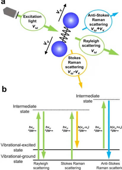
2.2 Raman spectroscopy
Raman spectroscopy involves the observation of scattered rather than emitted light. In this technique, irradiation of a specimen results in absorption, reflection, refraction and scattering based on the interaction between the light and the material. Both elastic and inelastic scattering can occur, and are referred to as Rayleigh and Raman scattering. In the case of elastic scattering, light of the same wavelength as the incident light is scattered, while inelastic scattering results in a frequency shift. The Raman scattered light is also 10
-6times weaker than Rayleigh scattered light. The Raman effect occurs due to an energy exchange between incident photons and the sample, and the frequency shift will vary according to the vibrational, rotational and electronic energy levels of the material.
Because each compound will have specific vibrational frequencies based on its structure, Raman spectroscopy employing a monochromatic laser light source can be used for characterization purposes.
Figure 2.3 presents a schematic illustration of the Raman scattering process and of the associated band structures for optical transitions in Raman scattering. In this technique, both Stokes and anti-Stokes scattering can occur. Stokes scattering, which reduces the light frequency compared to that of the incident light, involves transitions from the vibrational ground state to various excited states. In contrast, anti-Stokes scattering, which increases the frequency, is due to transitions from vibrational excited states to the ground state through intermediate states. Therefore, the intensity ratio of the Stokes/anti- Stokes scattering components of the Raman scattering reflects the probability that the material assumes specific vibrational excited states. At room temperature, samples are generally almost entirely in the vibrational ground state, and so Stokes scattering is much more common than anti-Stokes scattering. Therefore, Raman scattering typically generates reduced frequencies compared with that of the incident laser light, and spectra are displayed with the shift value from the frequency of the incident light (the Raman shift) on the abscissa axis.
If the incident light wavelength equals the energy of an electron absorption band, the
resulting resonance effect greatly increases the scattered light intensity, as the vibrational
transition is coupled with an electronic transition. This phenomenon allows a technique
21
termed resonance Raman spectroscopy and the associated intensity can be calculated based on the density of coupled states using the optically-allowed transition 𝑔(𝐸) [
42] as
𝐼(𝐸
𝑙) = ∫ |𝑀
(𝐸 𝑔(𝐸)𝑙−𝐸−𝑖Γ𝑟)(𝐸𝑙±𝐸𝑝ℎ−𝐸−𝑖Γ𝑟)
|
2
𝑑𝐸.
Here, 𝐸
𝑙is the photon energy of the excitation laser, 𝐸
𝑝ℎis the phonon energy, Γ
𝑟is the decay constant, and the − (+ ) symbol indicates Stokes (anti-Stokes) scattering.
Under resonance conditions, the denominator becomes zero and diverges, such that the Raman intensity become 1000 times larger. In the case of TMDCs, green light with a wavelength of 532 nm is utilized for resonance Raman spectroscopy.
Figure 2.3 (a) Schematic illustration of the Raman process and (b) a model of the band structures and transitions associated with Raman scattering.
22
Figure 2.4 shows the major Raman modes generated by MoS
2and WS
2, which are the E' mode and A
1' modes. The E' mode is due to vibrations in the in-plane direction, while the A
1' mode results from vibrations perpendicular to the plane direction. The layer numbers in WS
2and MoS
2specimens can be estimated based on the difference between the positions of these two modes. [
20, 43]
Figure 2.4 (a) Raman spectra of WS2 (blue) and MoS2 (red) and (b) a schematic illustration of the E’ and A1’ vibrational modes.
2.3 Scanning tunneling microscopy and spectroscopy
To investigate the structure and the electronic states of synthesized samples, we conducted
STM and STS observations. STM is a form of microscopy that generates images by
detecting the tunnel current flowing between a metal probe and a sample (Fig. 2.5a). STS
is a method of measuring the surface local density of states (LDOS) with nanoscale spatial
resolution by measuring the bias voltage-tunneling current characteristics of each part of
the sample while scanning the position of the STM probe. When a tip composed of a
metal such as tungsten and having a sharp point is brought sufficiently close to a sample
such that the electron clouds overlap, and a minute bias voltage is applied, electrons are
transferred by the tunneling effect and a current flows between the metal probe and
sample (Fig. 2.5b).
23
The tunneling current, I
t, is proportional to the product of the LDOS of the tip and the sample surface ( ρ
tand ρ
s) [
44-46].
𝐼(𝑉) ∝ ∫𝐸𝐸𝐹+𝑒𝑉𝜌𝑠(𝐸)𝜌𝑡(𝐸 + 𝑒𝑉)
𝐹 𝑑𝐸, (1)
where V is
the bias voltage between the tip and sample.
Equation (1) represents the total sum of the tunneling currents flowing from the probe occupancy level, ρ
t(-eV ≤ E ≤ 0), to the empty level, ρ
s(0 ≤ E ≤ eV), of the sample in response to the bias voltage, V. So that, if the LDOS of the probe tip is constant around Fermi level, E
F, the tunneling conductance can be expressed as
𝑑𝐼 𝑑𝑉⁄ ∝ 𝜌𝑠(𝑟, 𝐸). (2)
Equation (2) shows that the tunneling conductance is proportional to ρ
s(r, E
F) when the bias voltage, V, is small. Therefore, if the STM probe is scanned along the sample surface so as to keep the tunneling current constant, a constant electronic state (that is, a constant current image) will be obtained at the sample surface[
47-48]. Because the tunneling current changes exponentially with respect to the distance between the probe and the sample, the tunneling current will vary greatly even if that distance is only one half of an atom. Thus, the surface morphology can be observed with atomic resolution based on the tunneling current. The tunneling current also depends on the material, the atoms that are present and their electronic states, so it is possible to detect differences in chemical composition or changes in electronic states.
Furthermore, STS is conducted by measuring the tunneling current while varying the
bias voltage over different regions during scanning of the sample with the probe. In this
manner, STS can detect the unoccupied LDOS of the surface with atomic level spatial
resolution so as to visualize and evaluate electronic states, such as band gaps. In the
present work, we investigated the surface shapes and electronic states of specimens using
STM/STS in an ultra-high vacuum, employing a W tip.
24
Figure 2.5 (a) Schematic illustration of the STM measurement process and (b) and energy diagram of a tunneling barrier.
25
Chapter 3:
Growth and Optical Properties of
High-Quality Monolayer WS
2on Graphite
3.1 Introduction
TMDCs have attracted significant attention due to their fascinating chemical and physical properties[
3, 20] . In particular, monolayer Mo and W-based TMDCs (WSe
2, WS
2, MoSe
2, and MoS
2etc.), which become direct bandgap semiconductors, exhibit excellent on/off current ratios in FETs[
12, 49], strong PL[
7, 50-52], and unique spin-valley physics[
53-55].
Therefore, TMDCs are expected to be use for future electronics and optoelectronics devices[
20, 56]. However, the quality of available samples still causes serious problems, such as inhomogeneous lattice strain, structural defects, and charge doping. For example, high-resolution electron microscopy observes various structural defects, such as monosulfur and disulfur vacancies in TMDCs[
57]. PL spectra of as-exfoliated and CVD samples often show an asymmetric peak profile and multiple peaks that are probably caused by the presence of neutral free excitons, charged excitons (trions)[
9-10, 58-59], and/or defect-derived bound excitons[
9, 11]. Such charged and bound excitons also indicate that conventional samples have charged impurities and structural defects. Broad PL peak can also be caused by non-uniform lattice strain[
60]. Therefore, it is strongly required to develop a method for the preparation of high-quality TMDC samples.
Recently, many studies have been reported for the growth of high-quality TMDCs,
mainly using CVD and metal-film sulfurization[
13, 29-31, 61-66]. In particular, several groups
have used atomically-flat surfaces of graphite (or graphene) and hBN as the growth
substrates of TMDCs[
41, 62-66]. Monolayer WS
2grown by CVD on hBN was very recently
reported to exhibit a PL peak with a relatively narrow FWHM of 26 meV and a weak
asymmetric profile[
62]. Considering monolayer TMDC growth on commonly-used
substrates such as SiO
2/Si and sapphire, this indicates that the growth substrate is one of
the essential factors for reducing charged impurities and structural defects. Even though
26
such research has been tried for improving the growth conditions, the optical spectra of CVD samples are still much different from the high quality MoSe
2monolayers fabricated by mechanical exfoliation[
9]. This high-quality MoSe
2shows two PL peaks of neutral and charged excitons with a very narrow FWHM of 5 meV at 15 K for neutral exciton. These situations indicate that the CVD growth of high-quality TMDCs without carrier doping and structural defects is still the important issues.
Here, we report the growth of high-quality monolayer WS
2on a cleaved graphite surface by exceptionally high-temperature CVD at 1100 °C. The single-crystal domains are triangular shaped with sizes of up to 15 µm. PL and Raman spectroscopy reveal the uniformity and quality of WS
2samples grown on graphite, hBN, SiO
2/Si, and sapphire substrates. The PL spectra of WS
2samples grown on graphite have almost perfectly symmetric Lorentzian profiles and a narrow FWHM of 21 meV at room temperature and 8 meV at 79 K. Furthermore, there are no additional peaks due to charged and/or bound excitons, even at low temperature, which suggests that there are very few charged impurities and structural defects. These results indicate that the combination of high- temperature CVD with exfoliated graphite surface provides an ideal way for the growth of high-quality, non-doped TMDCs.
3.2 Experimental methods
Synthesis of monolayer WS
2Monolayer WS
2grains were grown on Kish graphite (Type C or B, Covalent Materials Co.), hBN, and c-plane sapphire (OS Tech Co., Ltd.) substrates using an improved CVD method[
13, 30-31], and on a SiO
2/Si (100 nm SiO
2) substrate by thin-film sulfurization[
41,61
]. Single-crystal hBN was prepared by a high-temperature and high-pressure method[
67].
Firstly, graphite and hBN crystals were mechanically exfoliated onto quartz substrates using Nitto tape (SPV-224).
For CVD growth, the substrates were placed in a quartz tube (3 cm diameter, 100 cm
long) with WO
3powder (Aldrich, 99% purity, 15–50 mg) and sulfur flakes (Aldrich,
99.99% purity, 2 g). The quartz tube was then filled with Ar gas at a flow rate of 100
27
cm
3/min. The temperature of the WO
3powder and the substrate was gradually increased to the sulfurization temperature (900–1100 °C) over 60 min using an electrical furnace.
When the substrate temperature was at the set point, the sulfur was heated at 200 °C for 15–30 min to supply sulfur vapor to the substrate using another electrical furnace. After sulfurization, the quartz tube was immediately cooled down using an electric fan. For the thin-film sulfurization method, the WO
3thin film was deposited onto a SiO
2/Si substrate in a striped shape using a shadow mask. The substrate was placed in the quartz tube with the sulfur flakes as previously described. The quartz tube was filled with Ar gas at a flow rate of 200 cm
3/min. The substrate and the sulfur were heated at 900 °C and 190 °C, respectively, for 30 min to conduct the sulfurization process. For the SiO
2/Si substrate, sulfurization was conducted at a lower temperature than the other substrates to avoid the reaction of Si and sulfur.
Characterizations
Optical images were recorded with an optical microscope (Nikon, Eclipse-LV100D).
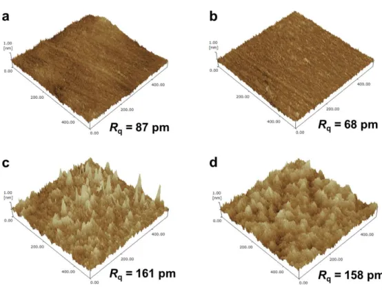
Raman measurements were conducted using a micro-Raman spectroscope (Renishaw, inVia) with an excitation laser at 532 nm. The temperature-dependent PL measurements were performed with a temperature-controlled microscope system (Linkam, THMS- 350V) in vacuum at 20 Pa. Topography images of the sample were obtained by using AFM (Shimadzu, SPM-9600) in tapping mode. Low-energy electron microscopy (LEEM) instrument (Elmitec LEEM III) was used to obtain bright-field and dark-field images, and Low-energy electron diffraction (LEED) patterns of WS
2on graphite. For assessment of sample structure, we conducted the high-resolution transmission electron microscopy (HRTEM). A cold field emission JEM-2100F equipped with a spherical aberration (Cs) corrector (the DELTA-corrector) was operated at 120 kV for the HRTEM imaging with high resolution and high contrast. The specimen was observed at room temperature. The Cs was set to less than 1 µm. A Gatan 894 CCD camera was used for digital recording of the HRTEM images. A sequence of HRTEM images (20 frames) was recorded, with an exposure time of 1 second for each. After drift compensation, some frames can be superimposed to increase the signal-to-noise (SN) ratio for display.
HRTEM images are filtered by a commercial software named HRTEM-Filters Pro.
28
3.3 Results and Discussions
3.3.1 Synthesis and crystal orientation of WS
2grown on graphite
Figure 3.1 (a) Optical image, (b) structural model, and (c) AFM image of monolayer WS2 grown on graphite. (d) Height profile of the dotted line in (c). (e) LEEM image and (f) LEED pattern of monolayer WS2 grown on graphite. The electron beam energies were 11 eV and 45 eV for LEEM and LEED observations, respectively. (g) Room-temperature PL spectra of monolayer WS2 grown on graphite, hBN, sapphire, and SiO2/Si substrates. There are two peaks, which are neutral exciton (Xo) and the lower-energy charged exciton (X-).
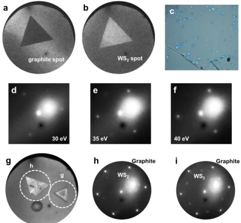
Figure 3.1a displays an optical image of triangular-shaped WS
2grains which have relatively dark contrast on graphite. The model image of this structure is shown in Fig.
3.1b. AFM observation reveals that a similar WS
2grain has uniform height of around 0.7
nm (Figs. 3.1c and d), which indicates these grains correspond to monolayer WS
2. Figure
3.1e shows a LEEM image of monolayer WS
2on graphite. The LEED pattern of this area
shows two hexagonal patterns which derived from the monolayer WS
2for the inner spots
and from graphite for the outer spots (Fig. 3.1f). This hexagonal pattern of the WS
2means
that such triangular-shape grains are single crystals, which is also confirmed from dark-
29
field LEEM images (Figs. 3.2a and b). Note that the LEED patterns become 3-fold symmetry depending on the electron beam energy, due to the symmetry of its crystal structure (Figs. 3.2d-f). These two hexagonal patterns clearly indicate that the monolayer WS
2crystal has the same crystal orientation as the graphite substrate.
In addition to the monolayer WS
2, multilayer WS
2grains are frequently observed on the graphite (Fig. 3.2g). On an optimized growth conditions, the ratio of monolayer to multilayer grains is roughly counted to be around 0.1. For the multilayer grains, LEEM and LEED results strongly suggest that they tend to have random orientation (Figs. 3.2g- i). These differences in the crystal orientation probably result from the nucleation process in the crystal growth.
Figure 3.2 Dark-field LEEM images constructed using diffraction spots of (a) graphite and (b)
monolayer WS2 in the LEED patterns. (c) Optical image of multilayer WS2 grains on graphite.
LEED patterns of the monolayer WS2 single crystal measured with the electron bean energies of (d) 30 eV, (e) 35 eV, and (f) 40 eV. (g) LEEM image of multilayer WS2 grains on graphite. (h,i) LEED patterns of multilayer WS2 in the selected area indicated by white circles in (g).
30
3.3.2 Substrate-dependent optical properties of WS
2Here, we will focus our attention on the optical properties and quality of monolayer WS
2grown on graphite and other substrates. Figure 3.3 shows typical room-temperature PL spectra for monolayer WS
2grown on graphite, hBN, sapphire and SiO
2/Si substrates.
Except for the hBN sample, the spectra were measured for triangular-shaped single crystals with sizes around 10 µm, as shown in Figs. 3.4a, 3.5a and 3.6a. Note that the monolayer WS
2crystals on hBN have mainly less than 1 μm size with the growth conditions employed, probably due to the different surface properties of hBN. On the SiO
2/Si substrates, WS
2crystals were grown by thin film sulfurization method at relatively-low temperature (900 °C) to avoid the reaction of Si with sulfur. These four spectra present PL peaks with different intensity, peak energies, linewidths, and profiles, as summarized in Table 3.1.
Figure 3.3 Room-temperature PL spectra of monolayer WS2 grown on graphite, hBN, sapphire, and SiO2/Si substrates. There are two peaks, which are neutral exciton (Xo) and the lower-energy charged exciton (X-).
31
Table 3.1 PL peak energies, PL FWHM, and E’ Raman modes for monolayer WS2 grown on graphite, hBN, sapphire, and SiO2 substrates.
Table 3.2 Fitting parameters of PL peaks for monolayer WS2 grown on graphite, hBN, sapphire, and SiO2 substrates.
The PL peaks of WS
2on graphite and hBN present similar symmetric profiles and small FWHMs. In contrast, asymmetric and broad PL peaks are observed in the case of WS
2on sapphire and SiO
2/Si. Only the PL spectrum for WS
2on graphite is well fitted by a single Lorentzian function, as shown in Fig. 3.3. For the other substrates, each peak can be reproduced by two Voigt function components. (The peak energies, FWHM, and peak- area ratios are given in Table 3.2.) For the asymmetric peaks, the components at lower and higher energies are assigned to the emission from trions and neutral free excitons, respectively[
9-10, 58-59]. The presence of both free excitons and trions indicates that there is local charge doping in the as-grown samples.
The FWHM values are 21, 22, 53 and 61 meV for the WS
2monolayers on graphite,
hBN, sapphire and SiO
2/Si, respectively. The WS
2grains on sapphire and SiO
2/Si have
comparable FWHM values to those previously reported for CVD-grown and exfoliated
monolayer WS
2on Si substrates[
40-41, 58]. In contrast, the FWHM values for the WS
2on
graphite and hBN are less than half, which suggests that there are fewer defects and
charged impurities in the WS
2. This is also supported by high resolution transmission
32
electron microscope (HRTEM) observations. As shown in Fig. 3.7, a clear lattice image and electron diffraction pattern are observed for few-layer WS
2grown on graphene. Even though the peak profiles are similar at room temperature, the spectra for on graphite and hBN measured at 79 K are much different, as discussed later.
For the PL intensities, the WS
2monolayers on hBN and SiO
2/Si exhibit comparable intense signals. On sapphire, the PL intensity decrease to around 1/6, which suggests relatively low sample quality of the WS
2on sapphire. It is noteworthy that the PL intensity of monolayer WS
2on graphite is two orders of magnitude less than that on hBN although they have almost the same FWHM values. This can be interpreted as the presence of a fast non-radiative recombination process of WS
2on graphite.
The dependence of the peak energy on the substrate is attributed to the effect of both lattice strain and dielectric screening. Dielectric screening is also known to affect the excitonic transition energy of other low-dimensional semiconductors, such as single-wall carbon nanotubes (SWCNTs)[
68]. The relative lattice strain is estimated from Raman measurements, as reported previously[
69-70]. PL and Raman mapping was conducted to investigate the uniformity within the single crystals in addition to the substrate effect.
Figure 3.4 (a) Optical image, (b) PL intensity and (c) peak wavelength maps, and (d) E’ Raman mode intensity and (e) peak wavenumber maps for monolayer WS2 grown on graphite. (f) PL and
33
(g) Raman spectra measured at three different points indicated by the symbols in (c) and (e), respectively.
Figure 3.5 (a) Optical image, (b) PL intensity and (c) peak wavelength maps, and (d) E’ Raman mode intensity and (e) peak wavenumber maps for monolayer WS2 grown on SiO2/Si. (f) PL and (g) Raman spectra measured at three different points indicated by the symbols in (c) and (e), respectively.
34
Figure 3.6 (a) Optical image, (b) PL intensity and (c) peak wavelength maps, and (d) E’ Raman mode intensity and (e) peak wavenumber maps for monolayer WS2 grown on sapphire. (f) PL and (g) Raman spectra measured at three different points indicated by the symbols in (c) and (e), respectively.