Direct Metal‐Free Chemical Vapor Deposition of Graphene Films on Insulating Substrates for Micro‐Supercapacitors with High Volumetric Capacitance
Author Michael Wuttke, Zhaoyang Liu, Hao Lu, Akimitsu Narita, Klaus Mullen
journal or
publication title
Batteries & Supercaps
volume 2
number 11
page range 929‑933
year 2019‑08‑25
Publisher Wiley‑VCH Verlag GmbH & Co. KGaA.
Rights (C) 2019 The Author(s) Author's flag publisher
URL http://id.nii.ac.jp/1394/00001292/
doi: info:doi/10.1002/batt.201900087
Creative Commons Attribution 4.0 International(https://creativecommons.org/licenses/by/4.0/)
1 2 3 4 5 6 7 8 9 10 11 12 13 14 15 16 17 18 19 20 21 22 23 24 25 26 27 28 29 30 31 32 33 34 35 36 37 38 39 40 41 42 43 44 45 46 47 48 49 50 51 52 53 54 55 56 57
Direct Metal-Free Chemical Vapor Deposition of Graphene Films on Insulating Substrates for Micro-Supercapacitors with High Volumetric Capacitance
Michael Wuttke
+,
[a]Zhaoyang Liu
+,
[a]Hao Lu,
[a]Akimitsu Narita,*
[a, b]and Klaus Müllen*
[a, c]Direct, metal-free synthesis of graphene films on insulating substrates in a controlled manner is of great importance for applications in (opto)electronic and energy storage devices.
Graphene films are fabricated on fused silica substrates without metal catalyst via chemical vapor deposition (CVD), using propionic acid as a carbon source. Film-thickness is readily adjustable between 5 and 45 nm by changing the deposition
time and flow rate of the precursor, displaying sheet resistance in the range of 0.27–1.86 kΩ
&1. The resulting graphene films are directly integrated into micro-supercapacitors without film transfer or liquid-phase processing, and demonstrate ultrahigh operation rates up to 1000 V s
1. Moreover, these films exhibit excellent rate capabilities, achieving a high volumetric capaci- tance of 131 F cm
3at 10 mV s
1.
1. Introduction
With the ever-increasing demand for portable and miniaturized electronics, lightweight, flexible, and highly efficient micro- scale energy storage systems are in high demand.
[1–3]Among them, micro-supercapacitors (MSCs) are particularly promising since they combine high power density with fast charge/
discharge rates and long cycle lives.
[4–6]Graphene is attractive as the active component of efficient MSCs because of its superior electrical conductivity, high specific surface area, and outstanding intrinsic double-layer capacitance. However, fab- rication of high-performance MSCs based on graphene films has remained elusive, because they tend to have low volumetric capacitance.
[7,8]The limited performance can be attributed largely to the lack of proper thickness control on suitable substrates over large areas
[9,10]and/or to relatively poor electronic properties of graphene samples used for MSCs.
[7,11,12]Thickness and electronic properties of graphene films are largely determined by the fabrication method. Graphene samples used for the MSC applications have typically been prepared using electrochemical exfoliation of graphite,
[13]chemical reduction of graphene oxide (rGO),
[14]and chemical vapor deposition (CVD).
[15]Films of electrochemically exfoliated graphene (EG) are prepared through filtration of its dispersion in isopropanol with membrane filters, followed by transfer onto desired substrates. Film thickness can be controlled by changing the concentration and/or amount of the dispersion.
However, MSCs prepared with such EG films exhibit poor performance, presumably due to the relatively low electronic conductivity of the films, which compromises the electrical double-layer capacitance.
[11,16,17]Performance can be improved by introducing additional pseudocapacitive conducting poly- mers, such as poly(3,4-ethylenedioxy thiophene):poly(styrene- sulfonate) (PEDOT: PSS) and polyaniline (PANI), but volumetric capacitance remains below 100 F cm
3.
[8,9]MSCs based on rGO films generally display even worse device performance com- pared with MSCs utilizing EG films, with volumetric capacitan- ces below 20 F cm
3.
[11,17]In contrast, graphene films prepared by the CVD method have higher quality with fewer structural defects and better electronic properties, which are advanta- geous for fabrication of high-performance MSCs.
CVD graphene films are mainly prepared through metal- catalyzed processes using copper foils as substrates, which can easily be scaled up to large areas or incorporated into roll-to- roll processes.
[18,19]Nevertheless, it is difficult to cleanly transfer the films from the metal surface to desired substrates (e. g., dielectrics, insulators) for further applications.
[20]Post-growth film transfer is carried out by etching the metal catalysts while using a polymer support, which inevitably compromises the quality of the graphene films, inducing, e. g., breaks, wrinkles, and contaminants of the surface with polymer residues. To this end, many attempts have been made to grow graphene films directly on insulating substrates without metal catalysts, for example, by applying techniques such as atmospheric pressure
[a] M. Wuttke,+Dr. Z. Liu,+Dr. H. Lu, Dr. A. Narita, Prof. Dr. K. MüllenMax Planck Institute for Polymer Research Ackermannweg 10, D-55128 Mainz, Germany E-mail: [email protected]
[email protected] [b] Dr. A. Narita
Organic and Carbon Nanomaterials Unit
Okinawa Institute of Science and Technology Graduate University 1919-1 Tancha, Onna-son, Kunigami, Okinawa, 904-0495, Japan [c] Prof. Dr. K. Müllen
Institute of Physical Chemistry Johannes Gutenberg-University Mainz Duesbergweg 10–14, 55128 Mainz, Germany [+] These authors contributed equally to this work.
Supporting information for this article is available on the WWW under https://doi.org/10.1002/batt.201900087
This publication is part of a joint Special Issue with ChemSusChem focusing on “2D Energy Storage Materials”.
© 2019 The Authors. Published by Wiley-VCH Verlag GmbH & Co. KGaA.
This is an open access article under the terms of the Creative Commons Attribution License, which permits use, distribution and reproduction in any medium, provided the original work is properly cited.
1 2 3 4 5 6 7 8 9 10 11 12 13 14 15 16 17 18 19 20 21 22 23 24 25 26 27 28 29 30 31 32 33 34 35 36 37 38 39 40 41 42 43 44 45 46 47 48 49 50 51 52 53 54 55 56 57
CVD (APCVD)
[21–23]and plasma-enhanced CVD (PECVD).
[24–27]However, transfer-free routes by direct CVD growth still suffer multiple drawbacks, including inhomogeneous nucleation at the macroscopic level, which results in small graphene domain sizes and poor film qualities. Moreover, the applications of graphene films produced by direct growth approaches have been limited to transparent conductive electrodes. Fabrication of high-quality graphene films with tunable thickness using the direct CVD approach, and its application to energy storage devices such as MSCs has remained elusive.
Here we demonstrate direct growth of CVD graphene on insulating fused silica substrates, using propionic acid as a precursor, and its integration into all-solid-state MSCs. By optimizing the low-pressure CVD (LPCVD) process, we were able to tune the thickness, optical transparencies, and electrical conductivities of the deposited graphene. We further fabricated MSCs using the as-grown graphene films on fused silica, which allowed operations at an ultrahigh rate up to 1000 V s
1, three orders of magnitude higher than conventional sandwich- structured electric double-layer capacitors. The device more- over exhibited an outstanding volumetric capacitance of 131 F cm
3at 10 mV s
1, and an excellent rate capability of 27 %, when operated from 10 to 10
5mV s
1.
2. Results and Discussion
Whereas molecules like methane have been used as precursors for direct growth of graphene on fused silica, we chose propionic acid, hypothesizing that a larger molecule with a lower decomposition temperature could be advantageous (decomposition temperature; methane: 1200
°C,
[28]propionic acid: 496
°C
[29]). The use of a carboxyl group appeared promising in view of previous density functional theory (DFT) studies, suggesting that the presence of oxygen-containing functional groups could enhance adsorption of hydrocarbons onto fused silica.
[30]Fused silica was selected as the substrate material due to its low cost and high softening point, which allow high-temperature growth on the substrate surface.
Graphene growth was achieved using a tube furnace with a diameter of 5 cm at a fixed temperature of 1100
°C. The fluid precursor was evaporated at a room temperature from a glass vial, connected by a valve. The vial containing the propionic acid was placed in a water bath to maintain the temperature during the evaporation. The evaporation of the precursor was controlled by adjusting the increase of the overall system pressure (Δp) after opening the valve. Raman spectra of the resulting graphene samples showed D, G, and 2D bands typical for turbostratic multilayer graphene.
[31]The G band is induced by the first-order scattering of the sp
2carbon, the D band by lattice defects and boundaries, and the 2D band results from second-order scattering of the D band.
[32]The 2D band of our as-grown graphene sample is observed at 2714 cm
1, without any shoulder, which is distinct from the 2D band of highly oriented pyrolytic graphite (HOPG) that is upshifted to 2739 cm
1with a shoulder appearing at 2704 cm
1(Fig- ure 1a).
[33]The 2D band of our sample also shows a broadening
presumably due to the relaxation of the double resonance Raman selection rules originating from the random orientation of the graphene layers, suggesting the existence of turbostratic multilayer graphene.
[31]Graphene quality could be greatly improved, based on the ratio of the D and G bands in Raman spectra (I
D/I
G),
[34]by increasing deposition time from 2 h to 3 h and by decreasing the amount of evaporated propionic acid by reducing the pressure increase (Table 1). Comparing the I
D/I
Gand I
2D/I
Gratios of sample 6 to graphene grown on copper substrates, EG
[9]and rGO (Table 2), it can clearly be seen that graphene grown on copper still owns the superior quality.
However, the I
D/I
Gand I
2D/I
Gratios of sample 6 is comparable to that of EG and superior to rGO, indicating the relatively high quality of graphene prepared by the current method.
Investigation of sample 6 by atomic force microscopy (AFM) revealed the growth of multi-layer graphene islands (Figure 1c) with an average height of ca. 4.1 nm, corresponding to approximately 11 layers, based on a layer thickness of 0.37 nm.
[35]UV-Vis transmission spectra revealed transmission of 80.4 % at 550 nm, which corresponds to 8.5 graphene layers, based on an absorbance of 2.3 % per layer.
[36]The discrepancy in the number of calculated layers from AFM images and transmission spectra can be attributed to the growth of multilayer graphene islands, which can be seen in the AFM image and the optical microscope image (Figure 1c–
d). Transmission spectroscopy and four-probe measurements of graphene films grown directly on fused silica (Figure 1b) show a direct correlation between the number of layers and the sheet resistance of the samples. Sheet resistances could be tailored within a range from 0.27–1.86 kΩ&
1by adjusting
Δp.The thinnest graphene film grown by the current method exhibits a transmittance of 86.1 %, corresponding to ~ 6 layers, and an average sheet resistance of 1.86 kΩ&
1, whereas the thickest film exhibits a transmittance of 22.3 %, corresponding to ~ 34 layers, and an average sheet resistance of 0.27 kΩ&
1. The graphene film was further characterized by X-ray Photoelectron Spectroscopy (XPS) verifying that no metal species exist in the resulting samples. The survey spectrum (Figure 2) displays predominant C 1s peaks from graphene, together with additional (O 1s, Si 2s, Si 2p) emissions from the
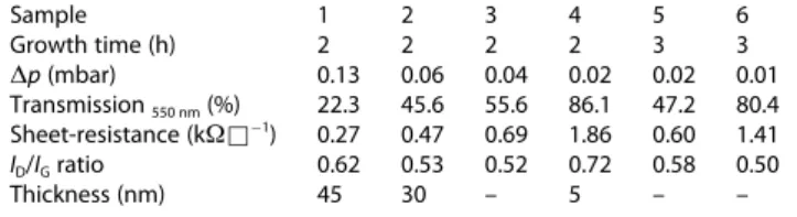
Table 1. Growth time and pressure increase (Δp) during preparation of graphene samples and their sheet-resistance, transmittance andID/IGratio.Sample 1 2 3 4 5 6
Growth time (h) 2 2 2 2 3 3
Δp(mbar) 0.13 0.06 0.04 0.02 0.02 0.01
Transmission550 nm(%) 22.3 45.6 55.6 86.1 47.2 80.4 Sheet-resistance (kΩ&1) 0.27 0.47 0.69 1.86 0.60 1.41
ID/IGratio 0.62 0.53 0.52 0.72 0.58 0.50
Thickness (nm) 45 30 – 5 – –
Table 2. Comparison of ID/IG and I2D/IG of the as-grown sample 6 with graphene grown on copper, EG and rGO calculated from Raman spectrum (Figure S2)
Sample 6 Graphene grown on copper EG rGO
ID/IG 0.50 / 0.41 0.95
I2D/IG 0.48 1.63 0.29 /
Articles
930
Batteries & Supercaps2019,2, 929 – 933 www.batteries-supercaps.org © 2019 The Authors. Published by Wiley-VCH Verlag GmbH & Co. KGaA
1 2 3 4 5 6 7 8 9 10 11 12 13 14 15 16 17 18 19 20 21 22 23 24 25 26 27 28 29 30 31 32 33 34 35 36 37 38 39 40 41 42 43 44 45 46 47 48 49 50 51 52 53 54 55 56 57
fused silica substrate. No trace of metal species can be detected, which is further verified by detailed XP spectra in the corresponding binding energy range (Figure S1). The high- resolution C 1s spectrum is self-fitted by individual emission peaks at binding energies of 284.1, 285 and 286.3 eV, which are assigned to sp
2carbon (cyan), sp
3carbon (blue) and C OH (green) bonds, respectively (Figure 2).
[37–39]The ratio of sp
2and sp
3carbon has been determined by further quantitative analysis from the C1s-spectrum. The resulting ratios of 85.5 %
sp
2, 11.5 % sp
3and only 3.1 % C OH indicate the high quality of the as-grown graphene films (Table S1).
Our graphene samples grown directly on fused silica substrates, with sheet resistances of 0.27–1.86
Ω& 1, are still inferior to bi-layer graphene grown by CVD on SiC substrates, with sheet resistances of 150
Ω&1,
[40]or single-layer graphene grown on metals, especially on Cu substrates, which show an even lower sheet resistance of 125
Ω&1with 97.4 % optical transmittance.
[19]Nevertheless, graphene samples with approx- imately 80 % transmittance produced by the current method exhibited a sheet resistance of ca. 1.4 kΩ&
1, which is superior to those of rGO films on glass (82 % transparency; 8 kΩ&
1)
[41]and graphene films grown directly on fused silica using PECVD (77–82 % transparency; 2.5–4.0 kΩ&
1).
[26,42]They are compara- ble to those of graphene produced by APCVD on fused silica (80 % transparency; 1.5–2.0 kΩ&
1)
[21,22]and graphene grown by liquid precursor-based methods (83.5 % transparency;
1.3 kΩ&
1).
[43]The relatively high quality of graphene films from direct CVD growth in the current study prompted us to examine their applicability to MSC devices. Further, the tunable film thickness achievable by our method offers an effective way to optimize MSC performance. The resulting graphene samples also dis- played smooth surfaces (Figure 1d), which can promote
Figure 1.(a) Raman spectra of a graphene film grown directly on fused silica (red line; Sample 6 in Table 1) and HOPG (black line) (b) UV-Vis transmission spectra of graphene samples 1–4 and 6 (see Table 1) as grown on fused silica, displaying transmittance at 550 nm and sheet resistance. (c) AFM height image of the as-grown graphene of sample 6. Scale bar: 1μm; Inset: Height profile along the blue line. Scale of height is nm. (d) Optical microscope image of the graphene film of sample 6. Scale bar: 20μm; Magnification: 100 × .Figure 2.(left) XPS survey spectrum of sample 1. (right) Fitted C1s spectra of sample 1 showing sp2Carbon at 284.1 eV (cyan line), sp3Carbon at 285 eV (blue line) and C OH at 286.3 eV (green line).
1 2 3 4 5 6 7 8 9 10 11 12 13 14 15 16 17 18 19 20 21 22 23 24 25 26 27 28 29 30 31 32 33 34 35 36 37 38 39 40 41 42 43 44 45 46 47 48 49 50 51 52 53 54 55 56 57
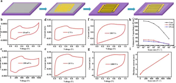
intimate contact between graphene electrodes and current collectors. Thus, we prepared all-solid-state MSCs based on graphene films with different thickness, i. e. 5 nm (sample 4), 30 nm (sample 2) and 40 nm (sample 1). MSCs were fabricated on fused silica substrates without the need of film transfer as illustrated in Figure 3a. Compared with MSC fabrication using EG and rGO, the current method avoids exfoliation and liquid- phase processing, which damage the graphene film.
To evaluate performance of MSCs fabricated by our method, cyclic voltammetry (CV) was performed at different scan rates ranging from 10 to 10
6mV s
1(Figure 3b-g). All CV curves revealed quasi-rectangular shapes from 0 to 1 V at scan rates of 10 to 10
4mV s
1. This indicates significant electrical double-layer capacitance from graphene because of the good electronic characteristics, i. e., relatively low sheet resistance ranging from 0.27 kΩ
& 1and 0.47 kΩ
& 1to 1.86 kΩ
& 1. Volumetric capacitances at different scan rates were calculated as previously reported for each sample with different film thickness and compared as displayed in Figure 3h.
[7–9]Remark- ably, for a 5-nm graphene film, a maximum areal capacitance of 66
μF cm 2and a volumetric capacitance of 131 F cm
3were delivered at a scan rate of 10 mV s
1. This outperformed most other MSCs based on graphene or porous carbon materials, with volumetric capacitances ranging from 1.3 to 17.9 F cm
3.
[7,11,17,44]When comparing the three graphene elec- trodes (Fig. 3 h), not surprisingly, volumetric capacitance decreased with increasing thickness. Such thickness-dependent behavior can be partially attributed to the limited interlayer conductivity of graphene films. Namely, thinner films can transport whole charges more efficiently to the gold current collector. The volumetric capacitance remained 35 F cm
3at a high scan rate of 10
6mV s
1, showing a capacitance retention of 27 %. Similarly, for 30-nm and 45-nm films, capacitance retention of 23 % and 26 % was demonstrated. These MSCs all allowed charge/discharge operations at ultrahigh rates up to 10
6mV s
1while maintaining excellent capacitance. This is three
orders of magnitude higher than conventional sandwich- structured electric double-layer capacitors and most reported high-power microdevices.
[7]Also, dependence of the discharge current on the scan rate was linear up to at least 10
5mV s
1(Figure 3i). Such excellent rate capability can be attributed to the fast ion diffusion and charge storage behavior, which preserved more than 20 % volumetric capacitance at high operating speeds. These results indicate that the direct CVD approach for graphene film production is promising for future powerful MSC applications.
3. Conclusions
In summary, we have developed a reliable new approach for direct graphene film deposition on fused silica using LPCVD.
Layer number and sheet resistance can be controlled by adjusting growth conditions. Graphene films directly grown on fused silica exhibit notable optical and electronic properties, with a transparency from 86 to 22 % at 550 nm and corresponding sheet resistances from 1.86 kΩ
& 1to 0.27 kΩ
&1. With graphene films synthesized under such carefully controlled conditions, we further fabricated MSCs employing the as-grown graphene films on fused silica substrates. The MSCs all allowed for operations at ultrahigh rates up to 1000 V s
1, which is three orders of magnitude higher than conventional sandwich-structured electric double- layer capacitors. High performance in regard to volumetric capacitance was delivered, with excellent rate capability. Such direct deposition of graphene films on desired substrates is crucial for future on-chip MSC devices, to avoid catalyst waste, fracturing of the graphene, and contamination during the transfer process. Although nucleation and growth mechanisms of graphene films on insulating substrates have yet to be addressed, further enhancement of the properties of graphene films and MSC performance can be expected by optimizing the
Figure 3.a) Schematic illustration of fabrication of MSC devices using CVD grown graphene films, b-g) CV curves of MSC based on sample 4 with scan rates ranging from 10 to 106mV s1, h) evolution of volumetric capacitances versus scan rates from graphene electrodes with different thickness, and i) plot of the discharge current as a function of the scan rate. Linear dependence is observed up to 100 V s1.
Articles
932
Batteries & Supercaps2019,2, 929 – 933 www.batteries-supercaps.org © 2019 The Authors. Published by Wiley-VCH Verlag GmbH & Co. KGaA
1 2 3 4 5 6 7 8 9 10 11 12 13 14 15 16 17 18 19 20 21 22 23 24 25 26 27 28 29 30 31 32 33 34 35 36 37 38 39 40 41 42 43 44 45 46 47 48 49 50 51 52 53 54 55 56 57
selection of precursor molecules and substrates, to create defined porous graphene structures suitable for MSCs.
Experimental Section
Growth of graphene: A quartz tube with an inner diameter of 4.5 cm was fixed in a single-zone electric furnace and heated to the desired temperature. Fused silica substrates were cleaned by sonication in dichloromethane for 10 min and then in deionized water (DI-water) for another 10 min. After cleaning, substrates were transferred to a horizontal quartz tube (5 cm diameter) placed inside a single-zone, high-temperature furnace. The system was evacuated and flushed with 10 sccm hydrogen for 5 min before starting to ramp the temperature. After reaching the desired temperature, graphene growth was initiated by opening the vial containing propionic acid. The propionic acid flow was controlled via the pressure increase in the system (Δp) by adjusting the opening of the vial. The typical pressure increase was between 0.02–0.13 mbar�0.01 mbar.
Fabrication of MSC: The graphene film was directly employed as the electrode material for MSCs without any additional treatment, followed by well-established lithography techniques to achieve interdigital microelectrode patterns through the deposition of gold as current collectors.[8] Then, an oxygen plasma was applied to remove excess graphene between the interdigital microelectrodes.
Finally, a polymer gel electrolyte H2SO4/polyvinyl alcohol (H2SO4/ PVA) was drop-cast onto the interdigital electrodes and allowed to solidify overnight, yielding the in-plane structured MSCs.
Acknowledgements
M.W. and Z.L. contributed equally to this work. This work was supported by the Max Planck Society and the European Union’s Horizon 2020 research and innovation program under grant agreement number 785219 (Graphene Flagship Core 2). We thank Steven D. Aird for editing the manuscript.
Conflict of Interest
The authors declare no conflict of interest.
Keywords:
direct chemical vapor deposition
·graphene
·volumetric capacitance
·micro-supercapacitors
·energy storage
[1] L. Wen, F. Li, H.-M. Cheng,Adv. Mater.2016,28, 4306–4337.
[2] C. Liu, F. Li, L.-P. Ma, H.-M. Cheng,Adv. Mater.2010,22, E28–E62.
[3] D. Qi, Y. Liu, Z. Liu, L. Zhang, X. Chen,Adv. Mater.2017,29, 1602802.
[4] M. Beidaghi, Y. Gogotsi,Energy Environ. Sci.2014,7, 867–884.
[5] N. A. Kyeremateng, T. Brousse, D. Pech,Nat. Nanotechnol.2016,12, 7.
[6] Z.-S. Wu, X. Feng, H.-M. Cheng,Natl. Sci. Rev.2013,1, 277–292.
[7] Z. Wu, K. Parvez, X. Feng, K. Müllen,Nat. Commun.2013,4, 2487.
[8] Z. Liu, S. Liu, R. Dong, S. Yang, H. Lu, A. Narita, X. Feng, K. Müllen,Small 2017,13, 1603388.
[9] Z. Liu, Z.-S. Wu, S. Yang, R. Dong, X. Feng, K. Müllen,Adv. Mater.2016, 28, 2217–2222.
[10] Z.-S. Wu, K. Parvez, S. Li, S. Yang, Z. Liu, S. Liu, X. Feng, K. Müllen,Adv.
Mater.2015,27, 4054–4061.
[11] M. F. El-Kady, R. B. Kaner,Nat. Commun.2013,4, 1475.
[12] M. F. El-Kady, V. Strong, S. Dubin, R. B. Kaner,Science2012,335, 1326–
1330.
[13] M. J. McAllister, J. L. Li, D. H. Adamson, H. C. Schniepp, A. A. Abdala, J.
Liu, M. Herrera-Alonso, D. L. Milius, R. Car, R. K. Prud’homme,Chem.
Mater.2007,19, 4396–4404.
[14] X. Cao, D. Qi, S. Yin, J. Bu, F. Li, C. F. Goh, S. Zhang, X. Chen,Adv. Mater.
2013,25, 2957–2962.
[15] A. Reina, X. Jia, J. Ho, D. Nezich, H. Son, V. Bulovic, M. S. Dresselhaus, J.
Kong,Nano Lett.2009,9, 30–35.
[16] M. F. El-Kady, Y. Shao, R. B. Kaner,Nat. Rev. Mater.2016,1, 16033.
[17] W. Gao, N. Singh, L. Song, Z. Liu, A. L. M. Reddy, L. Ci, R. Vajtai, Q.
Zhang, B. Wei, P. M. Ajayan,Nat. Nanotechnol.2011,6, 496.
[18] X. Li, W. Cai, J. An, S. Kim, J. Nah, D. Yang, R. Piner, A. Velamakanni, I.
Jung, E. Tutuc,Science2009,324, 1312–1314.
[19] S. Bae, H. Kim, Y. Lee, X. Xu, J.-S. Park, Y. Zheng, J. Balakrishnan, T. Lei, H. Ri Kim, Y. Il Song,Nat. Nanotechnol.2010,5, 574–578.
[20] J. W. Suk, A. Kitt, C. W. Magnuson, Y. Hao, S. Ahmed, J. An, A. K. Swan, B. B. Goldberg, R. S. Ruoff,ACS Nano2011,5, 6916–6924.
[21] J. Sun, Y. Chen, M. K. Priydarshi, Z. Chen, A. Bachmatiuk, Z. Zou, Z.
Chen, X. Song, Y. Gao, M. H. Rümmeli,Nano Lett.2015,15, 5846–5854.
[22] H. Bi, S. Sun, F. Huang, X. Xie, M. Jiang,J. Mater. Chem.2012,22, 411–
416.
[23] Y. Chen, J. Sun, J. Gao, F. Du, Q. Han, Y. Nie, Z. Chen, A. Bachmatiuk, M. K. Priydarshi, D. Ma,Adv. Mater.2015,27, 7839–7846.
[24] J. Sun, Y. Zhang, Z. Liu,ChemNanoMat2016,2, 9–18.
[25] D. Wei, Y. Lu, C. Han, T. Niu, W. Chen, A. T. S. Wee,Angew. Chem. Int. Ed.
2013,52, 14121–14126;Angew. Chem.2013,125, 14371–14376.
[26] L. Zhang, Z. Shi, Y. Wang, R. Yang, D. Shi, G. Zhang,Nano Res.2011,4, 315–321.
[27] J. Sun, Y. Chen, X. Cai, B. Ma, Z. Chen, M. K. Priydarshi, K. Chen, T. Gao, X. Song, Q. Ji,Nano Res.2015,8, 3496–3504.
[28] H. F. Abbas, W. M. A. Wan Daud,Int. J. Hydrogen Energy2010,35, 1160–
1190.
[29] P. G. Blake, K. J. Hole,J. Chem. Soc. B1966, 577–579.
[30] B. Liu, D.-M. Tang, C. Sun, C. Liu, W. Ren, F. Li, W.-J. Yu, L.-C. Yin, L.
Zhang, C. Jiang,J. Am. Chem. Soc.2011,133, 197–199.
[31] L. M. Malard, M. A. Pimenta, G. Dresselhaus, M. S. Dresselhaus, Phys.
Rep.2009,473, 51–87.
[32] A. C. Ferrari, D. M. Basko,Nat. Nanotechnol.2013,8, 235–246.
[33] L. G. Cançado, A. Reina, J. Kong, M. S. Dresselhaus,Phys. Rev. B2008,77, 245408.
[34] L. G. Cançado, K. Takai, T. Enoki, M. Endo, Y. A. Kim, H. Mizusaki, A. Jorio, L. N. Coelho, R. Magalhães-Paniago, M. A. Pimenta, Appl. Phys. Lett.
2006,88, 163106.
[35] H. Jussila, H. Yang, N. Granqvist, Z. Sun,Optica2016,3, 151–158.
[36] R. R. Nair, P. Blake, A. N. Grigorenko, K. S. Novoselov, T. J. Booth, T.
Stauber, N. M. R. Peres, A. K. Geim,Science2008,320, 1308.
[37] B. D. Ratner, D. G. Castner, inSurf. Anal. Princ. Tech.(Ed.: I. S. G. John C.
Vickerman), John Wiley & Sons Ltd, Chichester,2009, pp. 47–113.
[38] I. Cebula, H. Lu, M. Zharnikov, M. Buck,Chem. Sci.2013,4, 4455–4464.
[39] S. Ghosh, K. Ganesan, S. R. Polaki, T. R. Ravindran, N. G. Krishna, M.
Kamruddin, A. K. Tyagi,J. Raman Spectrosc.2014,45, 642–649.
[40] T. Ciuk, S. Cakmakyapan, E. Ozbay, P. Caban, K. Grodecki, A. Krajewska, I. Pasternak, J. Szmidt, W. Strupinski,J. Appl. Phys.2014,116, 123708.
[41] X. Li, G. Zhang, X. Bai, X. Sun, X. Wang, E. Wang, H. Dai, Nat.
Nanotechnol.2008,3, 538–542.
[42] H. Medina, Y.-C. Lin, C. Jin, C.-C. Lu, C.-H. Yeh, K.-P. Huang, K. Suenaga, J. Robertson, P.-W. Chiu,Adv. Funct. Mater.2012,22, 2123–2128.
[43] X. Chen, Z. Chen, W. Jiang, C. Zhang, J. Sun, H. Wang, W. Xin, L. Lin, M. K. Priydarshi, H. Yang,Adv. Mater.2017,29, 1603428.
[44] D. Pech, M. Brunet, H. Durou, P. Huang, V. Mochalin, Y. Gogotsi, P.-L.
Taberna, P. Simon,Nat. Nanotechnol.2010,5, 651.
Manuscript received: June 18, 2019 Revised manuscript received: August 2, 2019 Accepted manuscript online: August 6, 2019 Version of record online: August 25, 2019