Japan Advanced Institute of Science and Technology
JAIST Repository
https://dspace.jaist.ac.jp/
Title
Output properties of C_<60> field-effect
transistor device with Eu source/drain electrodes
Author(s)
Ochi, Kenji; Nagano, Takayuki; Ohta, Toshio;
Nouchi, Ryo; Kubozono, Yoshihiro; Matsuoka,
Yukitaka; Shikoh, Eiji; Fujiwara, Akihiko
Citation
Applied Physics Letters, 89(8): 083511-1-083511-3
Issue Date
2006-08-23
Type
Journal Article
Text version
publisher
URL
http://hdl.handle.net/10119/4509
Rights
Copyright 2006 American Institute of Physics.
This article may be downloaded for personal use
only. Any other use requires prior permission of
the author and the American Institute of Physics.
The following article appeared in K. Ochi, T.
Nagano, T. Ohta, , R. Nouchi, Y. Kubozono, Y.
Matsuoka, E. Shikoh, A. Fujiwara, Applied Physics
Letters, 89(8), 083511 (2006) and may be found at
http://link.aip.org/link/?APPLAB/89/083511/1
Output properties of C
60field-effect transistor device
with Eu source/drain electrodes
Kenji Ochi, Takayuki Nagano, Toshio Ohta, Ryo Nouchi, and Yoshihiro Kubozonoa兲
Department of Chemistry, Okayama University, Okayama 700-8530, Japan and CREST, Japan Science and Technology Agency, Kawaguchi 322-0012, Japan
Yukitaka Matsuoka, Eiji Shikoh, and Akihiko Fujiwara
Japan Institute of Science and Technology, Ishikawa 923-1292, Japan
and CREST, Japan Science and Technology Agency, Kawaguchi 322-0012, Japan
共Received 31 March 2006; accepted 30 June 2006; published online 23 August 2006兲
Field-effect transistor共FET兲 device with thin films of C60 has been fabricated with Eu electrodes exhibiting small work function. The C60 FET device shows n-channel FET properties with high field-effect mobility, 0.50 cm2V−1s−1. Furthermore, nonvanishing drain current, i.e., normally on, is observed in this FET device. This originates from small energy barrier for electron from Eu source electrode to lowest unoccupied molecular orbital of C60. © 2006 American Institute of Physics. 关DOI:10.1063/1.2337990兴
Field-effect transistor 共FET兲 devices with thin films of organic molecules have attracted special attention because of structural flexibility, low-temperature/low-cost processing, and large-area coverage.1,2The highest field-effect mobility value is 1.5 cm2V−1s−1 for the pentacene thin-film FET among FETs with organic thin films, and this device showed
p-channel normally off properties.3 On the other hand, the C60 and N , N
⬘
-dialkyl-3,4,9,10-perylene tetracalboxylic di-imide derivative thin-film FET devices showed n-channel normally off FET properties with the highvalues of 0.56– 0.65 and 0.6 cm2V−1s−1, respectively.4–6Very high values of 1 – 20 cm2V−1s−1 were reported for the FET devices with single crystals of rubrene and pentacene.7–10 Furthermore, p-channel, n-channel, and ambipolar FET devices with single crystals of rubrene and dibenzothiatetrathiafulvalene-tetracyanoquinodimethane were successfully fabricated by tuning the Fermi level of electrodes.11,12Thus, recent progress of organic single crystal FETs is dramatic and rapid. Nevertheless, it is indispensable to develop the thin-film FETs exhibiting excellent perfor-mance for practical applications of organic FETs. Especially,
n-channel FET devices exhibiting highvalues are required for design of complementary metal oxide semiconductor logic gate circuits because of the worse output properties for
n-channel thin-film FETs than those for p-channel FETs.
Recently, n-channel FET properties in the pentacene thin-film FET device were observed by using Ca metal for source/drain electrodes in the device; the value was quite low 共2.7⫻10−5cm2V−1s−1兲.13
No energy barrier for elec-tron exists from Ca electrodes 共Fermi energy14 EF= −=
−2.87 eV兲 to the lowest unoccupied molecular orbital 共LUMO兲 of pentacene 共energy level of LUMO, ELUMO= −3.2 eV兲.13This is probably the origin for the n-channel op-eration of the pentacene FET. Furthermore, the p-channel operation was realized in the C60thin-film FET by modifying Au electrodes with self-assembly monolayers.15 These re-sults show that the FET operation in the thin-film FET de-vices can also be controlled by using metal electrodes with various, as in the single crystals FET.11,12In this letter, we
have studied the output properties of C60 thin-film FET de-vices fabricated with metal electrodes exhibiting thevalue of 2.5– 5.65 eV. The C60 FET device with Eu source/drain electrodes14 共= 2.5 eV兲 showed the value of 0.50 cm2V−1s−1.
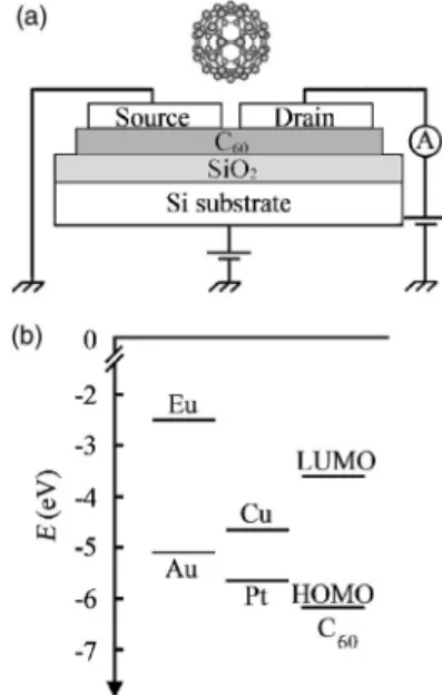
The C60 molecule and the top-contact-type device struc-ture are shown in Fig. 1共a兲; this device strucstruc-ture is adopted for Eu, while the bottom-contact-type device structure 共not shown兲 is adopted for Cu and Pt. Commercially available C60共99.98%兲 and SiO2/ Si共100兲 wafer were used for the for-mation of the active layers共thickness of 70–150 nm兲 and for a substrate, respectively. The SiO2 surface was treated with hexamethyldisilazane. During thermal deposition of C60 un-der 10−8Torr, the temperature of the substrate was main-tained at room temperature. Thickness of SiO2 layers was 400 nm, and the capacitance per unit area, C0, was deter-mined by LCR meter to be 7.3⫻10−9– 8.2⫻10−9F cm−2. The metal electrodes of 30– 50 nm thickness were attached as source/drain electrodes. The channel length L and the
a兲Electronic mail: [email protected] FIG. 1.FET.共b兲 Energy diagram of metals and LUMO and HOMO of C共a兲 Molecular structure of C60and device structure of C60thin-film 60.
APPLIED PHYSICS LETTERS 89, 083511共2006兲
0003-6951/2006/89共8兲/083511/3/$23.00 89, 083511-1 © 2006 American Institute of Physics Downloaded 10 Jun 2008 to 150.65.7.70. Redistribution subject to AIP license or copyright; see http://apl.aip.org/apl/copyright.jsp
channel width W of these devices were 50 and 4800m for Eu, respectively, and 30 and 2700m for Cu and Pt. The characteristics of the FET devices were measured in
n-channel measurement mode 关Fig. 1共a兲兴 under vacuum of
10−7Torr共Eu兲 or 10−6 Torr共Cu and Pt兲.
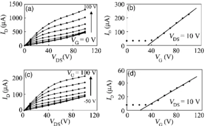
The plots of the drain current IDversus the drain-source voltage VDSin the C60FET device with Eu source/drain elec-trodes show n-channel normally on properties关Fig. 2共a兲兴; the C60 FET with Au source/drain electrodes showed n-channel normally off properties.4,16–18The EF for metals and the
en-ergy levels for LUMO and highest occupied molecular or-bital共HOMO兲 共ELUMOand EHOMO兲 are shown in Fig. 1共b兲; the EF values of metals, ELUMO, and EHOMOare taken from Refs. 8, 19, and 20. As the EFof Eu is higher than ELUMO, no energy barrier, i.e., Ohmic contact, for electron can be ex-pected between Eu electrode and LUMO. Actually, the inter-face dipole is known to be induced between metal electrodes and organic layers.21 In this case, the dipole shifts the vacuum level by the shift value⌬. The ⌬ value for Eu may be positive since the⌬ generally goes towards positive from negative with decreasing . The positive ⌬ may break Ohmic contact between the Eu electrodes and C60 thin films because the EFof Eu metal lowers by the⌬. However, as the
maximum⌬ is at most ⬃1 eV, the EF of Eu will become
⬃−3.5 eV 共=−2.5−⌬兲 even if ⌬=1 eV. Namely, the energy barrier between the Eu and C60 should be small even if the Schottky barrier is formed between Eu and LUMO level 共ELUMO= −3.6 eV兲 of C60. Consequently, nonvanishing ID observed at gate voltage VGof 0 V may be explained by no or small Schottky barrier when the C60 thin films contact to the Eu electrode.22
The and threshold voltage VT were determined to be
0.50 cm2V−1s−1and 34 V, respectively, from the ID-VGplot 关Fig. 2共b兲兴 at VDS= 10 V共linear region兲. Thevalue is com-parable to that, 0.56– 0.65 cm2V−1s−1, reported previously for the C60FET device with Au electrodes.4,6Thevalue of 0.56 cm2V−1s−1was observed for the FET device tested un-der 10−9Torr without exposure to air after formation of C60 thin films,4while theof 0.65 cm2V−1s−1was observed for the device tested under N2atmosphere共O2, H2O⬍0.1 ppm兲 without exposure to air.6The FET device with Eu electrodes fabricated in this study was exposed to air after formation of thin films of C60 and annealed at 363 K for 4 h under vacuum of 10−7Torr before formation of source/drain
elec-trodes. Here it should be noted that thevalues observed for the C60FET devices with Au electrodes after exposure to air could never get over 0.3 cm2V−1s−1 even when annealing them for ⬃12 h at 363–393 K under vacuum of 10−6– 10−8Torr, since deep trap states are formed in the channel region by adsorbed O2, and the transport of electrons are suppressed.16–18 Therefore, the value of 0.50 cm2V−1s−1for the C
60FET device exposed once to air can be closely related to the high injection efficiency of elec-trons from source electrode to LUMO achieved using Eu electrodes.
Here it is significant to say that the values are not independent of injected carrier concentration. As seen from Fig. 3共a兲, the total resistivitytof the C60FET device can be expressed with the resistivity ch of C60 thin films and the resistivity c between source/drain electrodes and C60 thin films as follows:
t=ch+c= 1/ench+c= 1/en. 共1兲
Here, e and n refer to the charge and carrier concentration. Thechcorresponds to the intrinsic mobility of thin films of C60. The c 共=s+d兲 can be associated with the Schottky
barrier between the electrodes and thin films;sandd
cor-respond to resistivity between source electrode and C60 thin films and resistivity between drain electrode and C60 thin films, respectively. As seen from Eq. 共1兲, the value in-creases with a decrease inc, showing that the value
re-flects strongly the injection efficiency from electrodes to C60 thin films. Such an increase invalue linked with injection efficiency is also found in the perylene FET device.23
Furthermore, it should be noted that the VT is positive
despite of nonvanishing IDat VG= 0 V. Generally, nonvan-ishing ID produces negative VT for n-channel operation. As
seen from Fig. 2共b兲, the IDis constant at⬃40A below VG of 40 V. This result implies that the IDof 40A does not correspond to channel current but bulk current which flows FIG. 2. 共a兲 ID-VDSplots and共b兲 ID-VG plot for C60 FET device with Eu
electrodes measured at 294 K just after annealing the device.共c兲 ID-VDS
plots and共d兲 ID-VGplot for C60FET devices with Eu electrodes measured at 294 K after keeping the device at 294 K for 12 h.
FIG. 3. 共a兲 Circuit model for the FET device. ID-VDSplots for C60 FET devices with共b兲 Cu and 共c兲 Pt electrodes measured at 294 K.
083511-2 Ochi et al. Appl. Phys. Lett. 89, 083511共2006兲
through the whole region of thin films. Namely, this device shows apparent normally on FET properties produced by high bulk current, and the bulk current originates from no or small energy barrier from source electrode to LUMO.
The IDvs VDSplots measured after keeping the device at 294 K for 12 h under vacuum of 10−8Torr is shown in Fig. 2共c兲. The IDdecreases by one order of magnitude, and the value was determined from the ID-VG plots 共linear region兲 shown in Fig. 2共d兲 to be 7.9⫻10−2cm2V−1s−1whose value is 1 / 6 of thevalue, 0.50 cm2V−1s−1, measured at 294 K just after annealing. The reduction of may be due to the oxidation of Eu electrodes. However, as the Eu electrode is top contacted to C60 thin films, further study is required to clarify whether the interface between the Eu electrodes and C60thin films is influenced by small amounts of O2.
The ID-VDSplots for the C60FET devices with Cu and Pt are shown in Figs. 3共b兲 and 3共c兲, respectively. These plots show n-channel normally off FET properties. As seen from Fig. 1共b兲, the energy barrier exists for electron between source electrode and LUMO level. This should lead to van-ishing IDat VGof 0 V since carriers cannot be injected be-cause of the impediment by the Schottky barrier. The val-ues for the C60 FETs with Cu and Pt were determined from the ID1/2-VG plots 共saturation region兲 to be 2.3⫻10−4 and 2.4⫻10−2cm2V−1s−1, respectively. The values for the C
60 FETs with Cu and Pt electrodes are smaller by one to three orders of magnitude than that of the C60FET device with Eu. The device structure is different between C60 FETs with Eu and Cu/ Pt. Though it is reported that the interface structure drastically changes between the pentacene thin films on metal electrodes and metal electrodes on pentacene thin films,24 the difference in output properties for the C60FETs with Eu and Cu/ Pt can be reasonably explained only by considering the difference in energy barrier between source electrode and C60 thin films.
The IDfor the C60FET with Cu electrodes关Fig. 3共b兲兴 is lower than that with Pt关Fig. 3共c兲兴 regardless of the smaller energy barrier between Cu and LUMO of C60 than that be-tween Pt and LUMO. Furthermore, the ID-VDSplots for the C60FET with Cu electrodes show nonlinear behavior at low
VDS, suggesting the existence of large Schottky barrier. These results present the possibility that the factors such as charge transfer and d −interaction between metal and C60 consid-erably change the netvalues of Cu and Pt metals.
In conclusion, the highvalue of 0.50 cm2V−1s−1 has been obtained in the C60FET device with Eu electrodes. The value is comparable to the best record obtained for the C60 FET device with Au electrodes fabricated without exposure to air.4,6 The ID-VDS plots for the C60 FET device with Eu electrodes show n-channel normally on property. These
re-sults are realized by high injection efficiency in electrons produced by no or small energy barrier for electron from source electrode to LUMO of C60.
The authors extend their appreciation to Y. Iwasa of In-stitute for Materials Research, Tohoku University for his valuable suggestion. This work is partly supported by a Grant-in-Aid共18340104兲 from MEXT, Japan.
1C. D. Dimitrakopoulos and D. J. Mascaro, IBM J. Res. Dev. 45, 11
共2001兲.
2C. D. Dimitrakopoulos and P. R. L. Malenfant, Adv. Mater.共Weinheim,
Ger.兲 14, 99 共2002兲.
3Y.-Y. Lin, D. J. Gundlach, S. F. Nelson, and T. N. Jackson, IEEE Electron
Device Lett. 18, 606共1997兲.
4S. Kobayashi, T. Takenobu, S. Mori, A. Fujiwara, and Y. Iwasa, Appl.
Phys. Lett. 82, 4581共2003兲.
5P. R. L. Malenfant, C. D. Dimitrakopoulos, J. D. Gelorme, L. L. Kosbar, T.
O. Graham, A. Curioni, and W. Andreoni, Appl. Phys. Lett. 80, 2517 共2002兲.
6J. N. Haddock, X. Zhang, B. Domercq, and B. Kippelen, Org. Electron. 6,
182共2005兲.
7V. Podzorov, V. M. Pudalov, and M. E. Gershenson, Appl. Phys. Lett. 82,
1739共2003兲.
8C. Goldmann, S. Haas, C. Krellner, K. P. Pernstich, D. J. Gundlach, and B.
Batllog, J. Appl. Phys. 96, 2080共2004兲.
9V. Podzolov, E. Menard, A. Borissov, A. Kiryukhin, J. A. Rogers, and M.
E. Gershenson, Phys. Rev. Lett. 93, 086602共2004兲.
10E. Menard, V. Podzorov, S.-H. Hur, A. Gaur, M. E. Gershenson, and J. A.
Rogers, Adv. Mater.共Weinheim, Ger.兲 16, 2097 共2004兲.
11T. Takahashi, T. Takenobu, J. Tkeya, and Y. Iwasa, Appl. Phys. Lett. 88,
033505共2006兲.
12Y. Takahashi, T. Hasegawa, Y. Abe, Y. Tokura, and G. Saito, Appl. Phys.
Lett. 88, 073504共2006兲.
13T. Yasuda, T. Goto, K. Fujita, and T. Tsutsui, Appl. Phys. Lett. 85, 2098
共2004兲.
14H. B. Michaelson, J. Appl. Phys. 48, 4729共1977兲.
15T. Nishikawa, S. Kobayashi, T. Nakanowatari, T. Mitani, T. Shimoda, Y.
Kubozono, G. Yamamoto, H. Ishii, M. Niwano, and Y. Iwasa, J. Appl. Phys. 97, 104509共2005兲.
16R. C. Haddon, A. S. Perel, R. C. Morris, T. T. M. Palstra, A. F. Hebard,
and R. M. Fleming, Appl. Phys. Lett. 67, 121共1995兲.
17K. Horiuchi, K. Nakada, S. Uchino, S. Hashii, A. Hashimoto, N. Aoki, Y.
Ochiai, and M. Shimizu, Appl. Phys. Lett. 81, 1911共2002兲.
18T. Kanbara, K. Shibata, S. Fujiki, Y. Kubozono, S. Kashino, T. Urisu, M.
Sakai, A. Fujiwara, R. Kumashiro, and K. Tanigaki, Chem. Phys. Lett. 379, 223共2003兲.
19N. Sato, Y. Saito, and H. Shinohara, Chem. Phys. 162, 433共1992兲. 20N. Hayashi, H. Ishii, Y. Ouchi, and K. Seki, J. Appl. Phys. 92, 3784
共2002兲.
21H. Ishii, N. Hayashi, E. Ito, Y. Washizu, K. Sugi, Y. Kimura, M. Niwano,
Y. Ouchi, and K. Seki, Phys. Status Solidi A 201, 1075共2004兲.
22S. M. Sze, Semiconductor Devices, Physics and Technology共Wiley, New
York, 2002兲, p. 224.
23T. Ohta, T. Nagano, K. Ochi, Y. Kubozono, E. Shikoh, and A. Fujiwara,
Appl. Phys. Lett. 89, 053508共2006兲.
24N. J. Watkins, L. Yan, and Y. Gao, Appl. Phys. Lett. 80, 4384共2002兲.
083511-3 Ochi et al. Appl. Phys. Lett. 89, 083511共2006兲