JAIST Repository
https://dspace.jaist.ac.jp/
Title
Optical, morphological, structural, electrical, molecular orientation, and electroluminescence characteristics of organic semiconductor films prepared at various deposition rates
Author(s) Matsushima, Toshinori; Shiomura, Koutaro; Naka, Shigeki; Murata, Hideyuki
Citation Thin Solid Films, 520(6): 2283-2288 Issue Date 2011-10-1
Type Journal Article
Text version author
URL http://hdl.handle.net/10119/10282
Rights
NOTICE: This is the author's version of a work accepted for publication by Elsevier. Toshinori Matsushima, Koutaro Shiomura, Shigeki Naka, Hideyuki Murata, Thin Solid Films, 520(6), 2011, 2283-2288,
http://dx.doi.org/10.1016/j.tsf.2011.09.060 Description
Optical, morphological, structural, electrical, molecular orientation, and
electroluminescence characteristics of organic semiconductor films prepared at
various deposition rates
Toshinori Matsushima a, Koutaro Shiomura a, Shigeki Naka b, Hideyuki Murata a,*
a
School of Materials Science, Japan Advanced Institute of Science and Technology,
1−1 Asahidai, Nomi, Ishikawa 923−1292, Japan
b
Graduate School of Science and Engineering, University of Toyama, 3190 Gofuku,
Toyama 930−8555, Japan
Keywords: Organic light−emitting diode, High deposition rate, Photoluminescence
quantum yield and lifetime, Time−of−flight charge carrier mobility, Molecular
orientation
ABSTRACT
Extremely high deposition rates of ≈7200 nm s−1 for
≈1700 nm s−1 for tris(8−hydroxyquinoline)aluminum (Alq3) are found to be possible by
controlling source−substrate distances and crucible temperatures. Shapes of ultraviolet−visible absorption spectra and photoluminescence (PL) spectra, atomic force
microscope images, X−ray diffraction patterns, PL quantum yields, PL lifetimes, and PL
radiative decay rates of the films remain independent of the deposition rates ranging
from 0.01 to 1000 nm s−1. On the other hands, hole currents of hole−only −NPD
devices increase ≈3 times while electron currents of electron−only Alq3 devices
decrease by ≈1/60 as the deposition rates are increased from 0.01 to 10 nm s−1. The
increase in hole current is confirmed to arise from an increase in hole mobility of
−NPD measured using a time−of−flight technique. The increase in hole moility is
probably due to a parallel orientation of an electronic transition moment of −NPD at
the higher deposition rates. Moreover, the three orders of magnitude increase in
deposition rate from 0.01 to 10 nm s−1 of −NPD and Alq3 results in a relatively small
increase in voltage of ≈15% and a decrease in external quantum efficiency of ≈30% in
organic light−emitting diodes (OLEDs). The reduction of the OLED performance is
attributable to the marked decrease in electron current relative to the slight increase in
hole current, indicating a decrease in charge balance factor at the higher deposition
* Corresponding author. Tel.: +81 761 51 1531; fax: +81 761 51 1149
1. Introduction
A vacuum thermal deposition technique used to manufacture multilayer organic
light−emitting diodes (OLEDs) based on small molecules [1] is inherently
time−consuming, resulting in the overall cost of manufacturing OLEDs greater than that
of manufacturing widely commercialized liquid crystal displays and plasma panel
displays. Constructing the multilayer OLED structure at a high deposition rate is
suggested to be an alternative way to reduce the tact time [2]. The deposition rates of
organic layers embedded into OLEDs are typically less than ≈0.1 nm s−1 and are
considered one of the key factors affecting performance of OLEDs. Indeed, Chen and
coworkers have shown that electron mobilities of tris(8−hydroxyquinoline)aluminum
(Alq3) decrease and power consumption of OLEDs increases by a small increase in
deposition rate of Alq3 from 0.2 to 0.7 nm s−1 [3]. Lie and coworkers have demonstrated
that electroluminescence (EL) efficiencies and operational lifetimes of OLEDs are
improved with increasing deposition rates of
bis(10−hydroxybenzo[h]qinolinato)beryllium (Bebq2) from 0.03 to 1.3 nm s−1 [4]. The
variation range of the deposition rates previously used to investigate device
performance is less than two orders of magnitude [3−7]. There has been still a lack of
performance of OLEDs are affected when the deposition rates are widely changed by
several orders of magnitude. In this study, we investigate the wide dependence of the
deposition rates of N,N´−diphenyl−N,N´−bis(1−naphthyl)−1,1´-biphenyl−4,4´−diamine
(−NPD) and Alq3 on their optical, morphological, structural, electrical, molecular
orientation, and EL characteristics.
2. Experimental details
Glass substrates coated with a 150 nm layer of indium tin oxide (ITO) and fused
silica substrates were cleaned using conventional ultrasonication, followed by
ultraviolet−ozone treatment. Organic films were vacuum−deposited on the substrates
under a pressure of ≈10−4 Pa using fused silica or carbon crucibles as deposition sources.
In our deposition setup, temperatures of the crucibles and distances between the crucible
and the substrate were controllable ranging in temperature from room temperature to
400 ºC and ranging in distance from 18 to 0.5 cm. Therefore, the deposition rates could
be six orders of magnitude changed from 0.001 to over 1000 nm s−1 by controlling the
source−substrate distances and the crucible temperatures. The deposition rates were
For optical, morphological, and structural characterizations, the films of −NPD
and Alq3 were vacuum−deposited on the fused silica substrates at the deposition rates
ranging from 0.01 to 1000 nm s−1 by controlling the source−substrate distances as well
as the crucible temperatures. The film thicknesses were set at 100 nm using the quartz
crystal microbalance in the case of the low deposition rates less than 10 nm s−1. When
the high deposition rates of 100 and 1000 nm s−1 were used, the resulting film
thicknesses were widely varied depending on the films due to extremely short
deposition times (for examples, 1 s for 100 nm s−1 and 0.1 s for 1000 nm s−1 to obtain
100 nm films). Thus, we prepared more than 10 films at the deposition rates of 100 and
1000 nm s−1 and measured their film thicknesses by stylus profilometry (Dektak 3030,
Veeco). The measured film thicknesses ranged from 90 to 750 nm. Among the films, we
chose the films having the thicknesses ranging from 100 to 150 nm for the optical,
morphological, and structural characterizations. The ultraviolet−visible (UV−vis)
absorption spectra, the photoluminescence (PL) spectra, the PL quantum yields, the PL
lifetimes, the surface morphologies, and the X−ray diffraction (XRD) patterns of the
films were measured respectively by using a V670 spectrometer (JASCO), a FP−6500
spectrometer (JASCO), a C9920 absolute PL quantum yield measurement system
atomic force microscope (AFM) (Seiko), and a M18XHF X−ray diffractometer (MAC
Science). The scan speeds of wavelength for the absorption and PL spectra were set at
100 nm s-1. The wavelengths of excitation light for the PL spectra and quantum yields
were set at 320 nm for −NPD and 370 nm for Alq3. A dynamic−force mode and a
standard uncoated cantilever (SI−DF20) were used for the AFM images. The transient
PL curves of −NPD and Alq3 at wavelengths of their absorption maxima were
measured under 378 nm pulse excitation light to estimate the PL lifetimes. The XRD
patterns were measured using a conventional 2/ technique with a CuK X−ray source
(=1.54 Å). All measurements were conducted at room temperature.
The hole−only and electron−only device structures were glass substrate/ITO
anode (150 nm)/MoO3 (0.75 nm)/-NPD (200 nm)/MoO3 electron−blocking layer (10
nm) [8]/Al cathode (100 nm) and glass substrate/ITO anode (150
nm)/2,9−dimethyl−4,7−diphenyl−1,10−phenanthroline (BCP) hole−blocking layer (30
nm)[9]/Alq3 (200 nm)/LiF electron−injection layer (0.5 nm) [10]/Al cathode (100 nm),
respectively [see the device structures shown in Figs. 1(a) and 1(b)]. Also, the OLED
structure was glass substrate/ITO anode (150 nm)/MoO3 buffer layer (0.75 nm)
layer (65 nm)[1]/LiF electron−injection layer (0.5 nm)/Al cathode (100 nm) as shown
in Fig. 1(c). To fabricate the devices, the deposition rates of −NPD and Alq3 were
changed from 0.01 to 10 nm s−1 by controlling the crucible temperatures while the
deposition rates of the other layers were set at constant: 0.05 nm s−1 for MoO3, 0.01 nm
s−1 for LiF, 0.5 nm s−1 for Al, and 0.1 nm s−1 for BCP. The source−substrate distance of
18 cm was used and the maximum deposition rate was limited to 10 nm s−1 to ensure
film uniformity and final film thickness. The current density−voltage−external quantum
efficiency characteristics and the EL spectra of the devices were measured as previously
reported [8,9].
3. Results and discussion
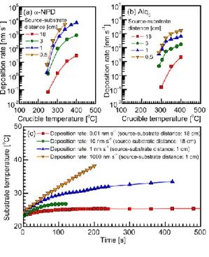
The deposition rate−crucible temperature characteristics of −NPD and Alq3 with
the different source−substrate distances are shown in Figs. 2(a) and 2(b), respectively.
The extremely high deposition rates of ≈7200 nm s−1 for −NPD (at a temperature of
400 ºC and a distance of 1 cm) and of ≈1700 nm s−1 for Alq3 (at a temperature of 400 ºC
and a distance of 0.5 cm) are found to be possible. The temperature of the substrate
surface during the −NPD deposition is recorded using a tiny thermocouple with a
use of the higher deposition rates and the shorter source−substrate distances results in
the more rapid increase in substrate temperature due to heating caused by a hot −NPD
vapor and a radiant ray from the crucible. The deposition times needed to obtain the 100
nm films are 10000 s for 0.01 nm s−1, 100 s for 1 nm s−1, 10 s for 10 nm s−1, and 0.1 s
for 1000 nm s−1. Within the deposition times, the substrate temperature increases by
only 2−6 ºC, so that the small variation of the substrate temperature would be less
influential for the film and device characteristics.
The increase in crucible temperature to obtain the high deposition rates may give
rise to a question that whether molecules are thermally decomposed or not during the
film deposition. Thus, the resulting films obtained at various crucible temperatures are
analyzed by means of high performance liquid chromatography (1100LC, Agilent) and
mass spectrometry (JMS−SX102A, JEOL). If molecules are thermally decomposed, it is
supposed that additional peaks are observed in the chromatography and mass spectra of
the high−deposition−rate films when compared with the source powders. However,
there is no detectable difference in their chromatography spectra between the films and
the source powders. The chromatography ensures the purity of the films greater than
molecules. The peak positions and the peak numbers of the mass spectra are similar
among the films, but the relative peak intensities are slightly different depending on the
films. Although we are not still on the place to decide whether thermally decomposed
species is present or not, we can only speculate from the results that the amount of
thermally decomposed species is not so large at the high crucible temperatures.
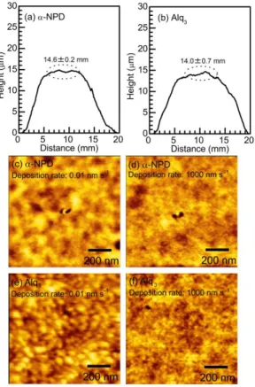
The cross sectional profiles of the films of −NPD and Alq3 prepared with the
high deposition rate of 500 nm s−1, the source−substrate distance of 1 cm, and the
deposition time of 30 s are measured using the stylus profilometry. The typical profiles
shown in Figs. 3(a) and Fig. 3(b) display a flat−top region from which the film
thicknesses are calculated to be 14.6±0.2 m for −NPD and 14.0±0.7 m for Alq3
respectively. The calculated thicknesses almost correspond to the expected thickness
(500 nm s−1×30 s=15 m). The AFM images and the optical spectra presented later are
measured in the flat−top regions of the high−deposition−rate films.
There is no obvious change in AFM image and surface roughness of −NPD and
Alq3 prepared at the deposition rates ranging from 0.01 to 1000 nm s−1. The
rates of 0.01 and 1000 nm s−1 are shown in Figs. 3(c)−(f). The films of −NPD and Alq3
have a small grain structure with grain diameters less than 50 nm. The average surface
roughnesses of the films are estimated to be 0.38±0.12 nm (−NPD) and 0.36±0.09 nm
(Alq3) from the AFM images of all films, which are slightly larger than that of
0.28±0.02 nm obtained from the optically polished quartz substrates. Moreover, results
of the XRD measurement using a conventional 2/ technique revealed that the
prepared films of −NPD and Alq3 had no diffraction peaks whereas there were intense
diffraction peaks from source powders of −NPD and Alq3 and vacuum−deposited
pentacene thin films [11], indicating amorphous film formation [7,11].
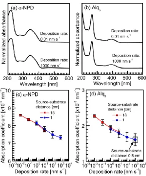
The representative UV−vis absorption spectra of the films of −NPD and Alq3
prepared at the deposition rates of 0.01 and 1000 nm s−1 are shown in Figs. 4(a) and
4(b), respectively. The absorption coefficients of −NPD and Alq3 are calculated by
dividing the peak absorbances at ≈350 nm (−NPD) and at ≈400 nm (Alq3) by the
actual film thicknesses measured by the stylus profilometry [Figs. 4(c) and 4(d)]. The
shapes of the UV−vis absorption spectra are independent of the deposition rates and
agree with those of previously reported spectra [12−14]. Despite the unchanged spectral
(Alq3) as the deposition rates are increased from 0.01 to 1000 nm s−1. The decrease in
absorption coefficient is indicative of a decrease in density of molecules, which may be
caused by unstable configuration of molecules in the films prepared at the higher
deposition rates.
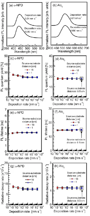
The representative PL spectra of the films of −NPD and Alq3 prepared at the
deposition rates of 0.01 and 1000 nm s−1, the PL quantum yield−deposition rate
characteristics, the PL lifetime−deposition rate characteristics, and the PL radiative
decay rate−deposition rate characteristics are shown in Fig. 5. The shapes of the PL
spectra and the obtained optical parameters remain independent of the deposition rates
as well and are in agreement with those reported previously [15−17]. Moreover, since
the two PL quantum yield−deposition rate curves obtained using the different
source−substrate distances and crucible temperatures are well overlapped, the films
have less exciton quencher generated by thermal decomposition.
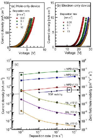
The current density−voltage characteristics of the hole−only −NPD devices and
the electron−only Alq3 devices are shown in Figs. 6(a) and 6(b), respectively (see the
characteristics are shown in Fig. 6(c). No EL is observed from the devices during the
current density−voltage measurements, indicating completely unipolar current flow.
When the deposition rates are increased from 0.01 to 10 nm s−1, the current densities of
the electron−only Alq3 devices decrease by ≈1/60, which agree with the decrease in
electron mobility of Alq3 reported in Ref. [3]. On the other hands, the current densities
of the hole−only −NPD devices reversely increase ≈3 times. This result is
contradictory to our expectation that the decrease in density of molecules [Figs. 4(c) and
4(d)] lowers probability of hopping transport between neighboring molecules.
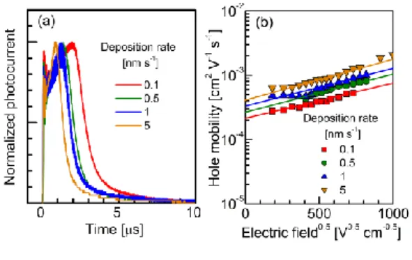
To investigate the increase in hole current observed in the −NPD devices, hole
mobilities of −NPD films prepared at various deposition rates are analyzed from a
glass substrate/ITO (150 nm)/Al (20 nm)/−NPD (3000 nm)/Al (200 nm) structure
using a time−of−flight (TOF) technique as previously reported in Ref. [18]. The TOF
hole transients of −NPD measured at an electric field of 2.7×10⁵ V cm−1 are shown in
Fig. 7(a). The transient currents somehow increase with time even if excitation light
powers are varied. Then, the transient currents suddenly drop because holes reach the
counter electrode. The hole transit time (tTR) is estimated from a change in slope in the
determined from the relationship =L2/(tTRV) [18], where L is the cathode−anode
spacing and V is the voltage. All −NPD films have field−dependent hole mobilities ()
as shown in Fig. 7(b). The field−dependent hole mobilities are expressed as
=0exp(E0.5) [3,18], where 0 is the zero field hole mobility, is the field dependence
parameter, and E is the electric field. The zero field hole mobilities of −NPD are found
to slightly increase as the deposition rates are increased [Fig. 6(c)], but the field
dependence parameters remain constant for all films (≈1.4×10⁻³ cm0.5 V-0.5). The
obtained values are similar to those previously reported (0=4.0×10⁻⁴ cm2 V−1 s−1 and
=1.1×10⁻³ cm0.5 V−0.5)[18]. Since the hole mobilities of −NPD are changed in the
manner similar to the current densities of the hole−only −NPD devices [Fig. 6(c)], the
increase in hole current arises from the increase in hole mobility.
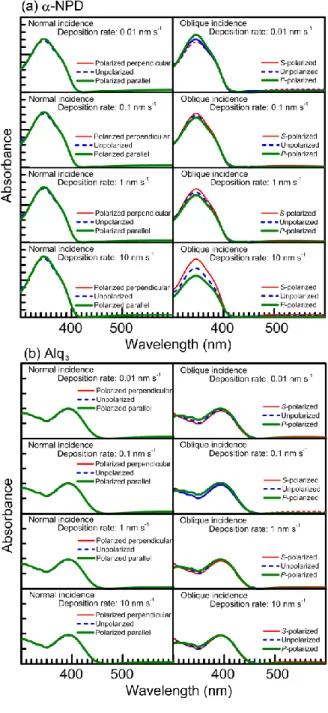
It has been reported recently that a molecular orientation occurs when growth
conditions of organic films are changed [19]. Thus, the films of −NPD and Alq3 are
vacuum−deposited on the fused silica substrates at the deposition rates of 0.01, 0.1, 1,
and 10 nm s−1 and their molecular orientations are evaluated using polarized absorption
spectra under normal and oblique (45°) light incidence [11] [Figs. 8(a) and 8(b)]. The
indicating that the Alq3 films are optically random in every direction [Fig. 8(b)]. There
is no polarized absorption from the −NPD films under the normal incidence as well
[Fig. 8(a)], indicating that −NPD molecules are in−plane random. However, for the
oblique incidence, the p−polarized absorbance is larger than the s−polarized absorbance
in the 0.01 nm s−1 −NPD film. And the p−polarized and s−polarized absorbances are
gradually reversed as the deposition rates are increased from 0.01 to 10 nm s−1. The
molecular orientation of −NPD is somewhat induced using the higher deposition rates
in the manner that the electronic transition moment direction is changed from normal to
parallel to the substrate. One tends to consider formation of a random molecule structure
at the higher deposition rates due to short−range surface migration of molecules, but the
obtained result is somehow opposite. The change in the molecular orientation of
−NPD could be related to the increase in hole current and hole mobility [Fig. 6(c)].
Moreover, the transition moment orientation parallel to the substrate increases the
absorbance by ≈15% because molecules with the parallel oriented transition moment
can absorb the normal−incidence light more strongly than the oblique−incidence light.
Thus, the decrease in absorption coefficient of −NPD (≈15%) is slower than that of
Alq3 (≈30%) [Figs. 4(c) and 4(d)], probably due to the parallel transition moment
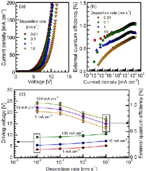
The current density−voltage and external quantum efficiency−current density
characteristics of the OLEDs prepared using the different deposition rates are shown in
Figs. 9(a) and 9(b), respectively [see the device structure shown in Fig. 1(c)]. The drive
voltages and the external quantum efficiencies at the current densities of 1, 10, and 100
mA cm−2 are plotted versus the deposition rates in Fig. 9(c). We observe an increase in
drive voltage and a decrease in external quantum efficiency as the deposition rates of
−NPD and Alq3 are increased [Fig. 9(c)]. Shapes of EL spectra of all OLEDs
(originating from electrically excited Alq3) remain independent of the deposition rates,
indicating that a carrier recombination zone is probably pinned near the -NPD/Alq3
interface. The maximum external quantum efficiency at the deposition rate of 0.1 nm s−1
and the shapes of the EL spectra correspond well with those previously reported [15,16].
The external quantum efficiencies (EXT) can be given by the equation [20,21],
EXT=OUTE/HEXCPL, where OUT is the light out−coupling efficiency, E/H is the
charge balance factor, EXC is the efficiency of single or triplet exciton generation, and
PL is the PL quantum yield. Since the exciton generation efficiencyis basically fixed at
be independent of the deposition rates due to the unchanged EL spectra, the observed
decrease in external quantum efficiency is therefore attributable to a decrease in either
charge balance factor or PL quantum yield. Since the PL quantum yields are unchanged
in the whole deposition rate region as can be seen in Figs. 5(c) and 5(d), we can
conclude that the PL quantum yields cause no influence on the external quantum
efficiencies of the OLEDs. On the other hands, the opposite changes in the current
density−deposition rate characteristics of the single−carrier devices in Fig. 6(c) suggest
that the increase in drive voltage and the decrease in external quantum efficiency of the
OLEDs are caused by the marked decrease in electron current relative to the slight
increase in hole current, meaning that the decrease in charge balance factor at the higher
deposition rates.
4. Summary
Optical, morphological, structural, electrical, molecular orientation, and EL
characteristics of organic films depending on organic deposition rates are investigated.
Shapes of UV−vis absorption spectra and PL spectra, AFM images, XRD patterns, PL
quantum yields, PL lifetimes, and PL radiative decay rates of films of −NPD and Alq3
other hands, hole currents of hole−only −NPD devices increase ≈3 times while
electron currents of electron−only Alq3 devices decrease by ≈1/60 when the deposition
rates are increased from 0.01 to 10 nm s−1. The increase in hole current is confirmed to
arise from an increase in hole mobility of −NPD measured using a TOF technique.
The increase in hole mobility is probably due to a parallel orientation of an electronic
transition moment of −NPD at the higher deposition rates. Moreover, we find that
drive voltages increase by ≈15% and external quantum efficiencies decrease by ≈30%
for OLEDs when the deposition rates of −NPD and Alq3 are increased from 0.01 to 10
nm s−1. From the results of the PL quantum yields and the current density−voltage
characteristics of the single−carrier devices, we can conclude that the decrease in
external quantum efficiency is attributable to the decrease in electron current relative to
the increase in hole current, which leads to a decrease in charge balance factor. Since
the decrease in electron current is more pronounced than the increase in hole current,
the drive voltages of the OLEDs are assumed to increase when the higher deposition
rates are used. This finding opens a way to fabrication of high−performance OLEDs at
high deposition rates if organic layers showing enhanced charge transport like −NPD
Acknowledgement
The authors are grateful to Prof. Hiroyuki Okada (University of Toyama) for
useful discussion and Dr. Hidetoshi Fujimura (FUJIFILM CO.) for measurements of
mass spectrometry and liquid chromatography. This work is supported by
Grants−in−Aid for Scientific Research (Grant Nos. 21760005, 20241034, and
20108012). Part of this work is based on “Development of the next generation
large−scale organic EL display basic technology (Green IT Project)” with New Energy
References
[1] C. W. Tang, S. A. VanSlyke, Appl. Phys. Lett. 51 (1987) 913.
[2] E. Matsumoto, S. Maki, Y. Yanagi, T. Nishinori, Y. Kondo, Y. Kishi, J. Kido, Society
for Information Display International Symposium, Digest of Technical Papers, 34
(2003) 1423.
[3] B. J. Chen, W. Y. Lai, Z. Q. Gao, C. S. Lee, S. T. Lee, W. A. Gambling, Appl. Phys.
Lett. 75 (1999) 4010.
[4] S.-W. Liu, C.-C. Lee, C.-H. Wang, J.-H. Lee, C.-T. Chen, J.-K. Wang, Chem. Phys.
Lett. 474 (2009) 207.
[5] Y. Qiu, D. Q. Zhang, J. Qiao, Y. Shao, Synth. Met. 110 (2000) 241.
[6] H. Mu, H. Shen, D. Klotzkin, Solid-State Electron. 48 (2004) 2085.
[7] P.-T. Lee, T.-Y. Chang, S.-Y. Chen, Org. Electron. 9 (2008) 916.
[8] T. Matsushima, G.-H. Jin, H. Murata, J. Appl. Phys. 104 (2008) 054501.
[9] T. Matsushima, M. Takamori, Y. Miyashita, Y. Honma, T. Tanaka, H. Aihara, H.
Murata, Org. Electron. 11 (2010) 16.
[10] L. S. Hung, C. W. Tang, M. G. Mason, Appl. Phys. Lett. 70 (1997) 152.
[11] T. Matsushima, H. Murata, Appl. Phys. Lett. 98 (2011) 253307.
[13] T. Matsushima, Y. Kinoshita, H. Murata, Appl. Phys. Lett. 91 (2007) 253504.
[14] D.-S. Leem, H.-D. Park, J.-W. Kang, J.-H. Lee, J. W. Kim, J.-J. Kim, Appl. Phys.
Lett. 91 (2007) 011113.
[15] G. Sakamoto, C. Adachi, T. Koyama, Y. Taniguchi, C. D. Merritt, H. Murata, Z. H.
Kafafi, Appl. Phys. Lett. 75 (1999) 766.
[16] T. Dobbertin, M. Kroeger, D. Heithecker, D. Schneider, D. Metzdorf, H. Neuner, E.
Becker, H.-H. Johannes, W. Kowalsky, Appl. Phys. Lett. 82 (2003) 284.
[17] Y. Kawamura, H. Sasabe, C. Adachi, Jpn. J. Appl. Phys. 43 (2004) 7729.
[18] S. Naka, H. Okada, H. Onnagawa, Y. Yamaguchi, T. Tsutsui, Synth. Met. 111−112
(2000) 331.
[19] D. Yokoyama, Y. Setoguchi, A. Sakaguchi, M. Suzuki, C. Adachi, Adv. Funct.
Mater. 20 (2010) 386.
[20] T. Tsutsui, Mater. Res. Soc. Bull. 22 (1997) 39.
[21] M. A. Baldo, D. F. O’Brien, M. E. Thompson, S. R. Forrest, Phys. Rev. B 60
Figure captions
Fig. 1. Schematic structures of (a) hole−only devices, (b) electron−only devices, and (c)
OLEDs.
Fig. 2. Deposition rate−crucible temperature characteristics of (a) −NPD and (b) Alq3
with different source−substrate distances and (c) substrate temperature−time
characteristics measured during −NPD deposition.
Fig. 3. Cross sectional profiles of films of (a) −NPD and (b) Alq3 prepared with
deposition rate of 500 nm s−1, source−substrate distance of 1 cm, and deposition time
of 30 s and AFM images of −NPD prepared at deposition rates of (c) 0.01 and (d)
1000 nm s−1 and of Alq3 prepared at deposition rates of (e) 0.01 and (f) 1000 nm s−1.
Fig. 4. UV-vis absorption spectra of (a) −NPD and (b) Alq3 prepared at deposition
rates of 0.01 and 1000 nm s−1 and absorption coefficient−deposition rate
characteristics of (c) −NPD and (d) Alq3.
1000 nm s−1, PL quantum yield−deposition rate characteristics of (c) −NPD and (d)
Alq3, PL lifetime−deposition rate characteristics of (e) −NPD and (f) Alq3, and PL
radiative decay rate−deposition rate characteristics of (g) −NPD and (h) Alq3.
Fig. 6. Current density−voltage characteristics of (a) hole−only −NPD devices and (b)
electron−only Alq3 devices and (c) current density−deposition rate characteristics at 1,
3, and 5 V (−NPD) and at 10, 13, and 15 V (Alq3) and TOF zero field hole
mobility−deposition rate characteristics of −NPD films..
Fig. 7. (a) TOF hole transients measured at electric field of 2.7×10⁵ V cm−1 and (b) hole
mobility−square root of electric field characteristics of −NPD prepared at different
deposition rates.
Fig. 8. Polarized UV-vis absorption spectra of (a) −NPD and (b) Alq3 measured under
normal and oblique light incidence. Deposition rates of −NPD and Alq3 are
changed from 0.01 to 0.1, 1 and 10 nm s−1.
characteristics of OLEDs prepared with different deposition rates and (c) drive
voltage−deposition rate and external quantum efficiency−deposition rate
Fig. 1
Matsushima
Fig. 2
Matsushima
Fig. 3
Matsushima
Fig. 4
Matsushima
Fig. 5
Matsushima
Fig. 6
Matsushima
Fig. 7
Matsushima
Fig. 8
Matsushima
Fig. 9
Matsushima