1
首都大学東京 博士(理学)学位論文(課程博士)
論 文 名 光機能性薄膜の作製と分子センサーへの応用(英文)
著 者 藤田 隆史
審査担当者 主 査 委 員 委 員 委 員
上記の論文を合格と判定する 平成 年 月 日
首都大学東京大学院理工学研究科教授会
研究科長
2
DISSERTATION FOR A DEGREE OF DOCTOR OF PHILOSOPHY IN SCIENCE
TOKYO METROPOLITAN UNIVERSITY
TITLE : Fabrication of optical functional thin film for an application as a molecular sensor
AUTHOR:Takashi Fujita
EXAMINED BY
Examiner in chief
Examiner
Examiner
Examiner
QUALIFIED BY THE GRADUATE SCHOOL OF SCIENCE AND ENGINEERING
TOKYO METROPOLITAN UNIVERSITY
Dean
Date
3
学位論文要旨(理学博士)
論文著者名 藤田 隆史
論文題名
Fabrication of optical functional thin film for an application as a molecular sensor
(邦題):光機能性薄膜の作製と分子センサーへの応用(英文)
Optical functional thin films can cause various surface effects by their photo excitation. These surface effects are divided into two types. One is surface reaction with adsorbate. The other is unique career movement such as surface plasmon (SP) excitation, charge separation and so on. These effects lead to various applicatons such as photocatalyst, solar cell, optical sensors and so on. Therefore, fabrication of optical functional thin films gives us not only scientific interest but also various practical uses.
In this thesis, the author fabricated two optical functional thin films (titania thin film and two dimensional array (2D-array) of gold nanoparticle) for application of optical molecular sensor with surface assisted laser desorption/ionization (SALDI-MS) and surface enhanced Raman scattering (SERS) measurements.
Photocatalytic effect on titania surface causes interesting reaction such as degradation of organic molecules and site-selective redox reaction and so on. However, these reactions are very complex. Therefore, simple observation methods for revealing these reaction products in whole are required. In order to observe these reaction products, the author focused on SALDI-MS because SALDI-MS spectra can reflect surface properties of SALDI-MS ionization substrates according to our previous studies.
In this thesis, the author fabricated titania thin film, and then applied the thin film to SALDI-MS substrates for monitoring degradation of organic molecules with oligosaccharides.
SERS is an attractive technique for ultra-trace analysis of analyte due to its huge enhancement effect caused by SP resonance on a metal nanostructured surface.
However, it is difficult to control the enhancement effect because the efficiency of SP
resonance strongly depends on a surface morphology of the SERS active substrate.
4
From this reason, conventional SERS measurement has not applied for practical optical molecular sensor due to its low-reproducibility. Therefore, in order to solve this problem, uniform surface morphology of nanostructure is required as a SERS active substrate. To create a uniform surface roughness of a nanostructured surface, the author focused on a highly-ordered 2D-array of metal nanoparticles (2DMA) with a constant inter-particle distance by using same metal nanoparticle because fabricated SERS active substrates are expected to have same enhancement effect at any position of the substrate.
Highly-ordered 2DMAs requires elimination of aggregations because aggregations cause not only a random efficiency of SP excitation but also a decrease of enhancement effect. Generally, in order to prevent nanoparticles from aggregating, surface modifier are used because the modifier plays a role as a spacer between nanoparticles. However, the surface modifier changes its optical property and generates background signals which interfere with the detection of target molecules. From these reasons, it is expected that the 2DMA composed by metal nanoparticles without any surface modifier has a large potential for a molecular sensor, but fabrication methods of the 2DMA still have not been proposed.
On the other hand, our group succeeded in fabrication of highly-ordered 2DMA without any surface modifier by using the novel technique, which is called sandwich (SW) method. The SW method is a very simple technique which is only by sandwiching the gold nanoparticle (AuNP) solution between two flat plates and drying naturally.
However, the 2DMA at this stage could not work for SERS analysis. The reason was that an area of the 2DMA was too small to obtain many SERS spectra from one substrate and to estimate the quantitative performance. In this thesis, the fabrication condition of the SW-method has been optimized in order to expand the area of the 2DMA and a fabrication mechanism in the SW-method has been studied. Then the 2DMA has been applied to SERS measurement in order to develop a molecular sensor with a high reproducibility and an ultra-high sensitivity.
Chapter 1 deals with general introduction. Importance of optical functional thin films was discussed. Proposed mechanisms of photocatalytic effect and SERS enhancement effect and purpose of this thesis are discussed.
In chapter 2, SALDI-MS measurements of oligosaccharides on the titania
substrate, which were prepared by using oil/water interface trapping method, were
discussed. A lot of fragment ions of oligosaccharides were observed. They had
periodical molecular weight which is correspond to oligosaccharide units only by our
substrate. It is suggested that the unique fragmentation process on the titania
SALDI-MS substrate relates to photocatalytic reaction.
5
In chapter 3, fundamentals of localized SP (LSP), calculation of optical properties of AuNPs and inter-particle coupling effect are discussed in order to understand a relationship between LSP excitation and electromagnetic enhancement in SERS. Optimum diameter of AuNP was estimated for the SERS measurement. To be from 60 nm to 100 nm are suitable because they have high efficiencies of SP excitation.
In chapter 4, common fabrication methods of two-dimensional metal nanostructure and the reason why attention was paid to the 2DMA as quantitative SERS active substrates are discussed. And, the theory for interactions between colloids in solution is discussed. As a result, a guideline for fabricating the highly-ordered 2DMA composed by AuNPs without any surface modifier was obtained.
In chapter 5, SW method and characterization of the 2DMA fabricated by SW method using scanning electron microscope are discussed. And, experimental conditions of the SW method were optimized. As a result, the area of the 2DMA composed by AuNPs without any surface modifier was expanded compared with that at early stage of this method. Moreover, the 2DMA had a higher packing rate compared with those fabricated by conventional methods.
In chapter 6, a uniformity of the 2DMA of the SW-method and a mechanism of arrangement in the SW-method are discussed by using SEM analysis with Fourier Transform analysis, Vis absorption spectroscopy and optical microscope. These analyses showed that the 2DMA had a high uniformity and a hexagonal periodicity with inter-particle distance of 4nm in the arrangement. From these results, it is considered that the 2DMA have a high uniformity and a constant inter-particle distance (4.5nm) which has a large potential to generate a giant enhancement effect. Moreover, the assembly mechanism of SW method was investigated by observations of assembly process with an optical microscope. As a result, it was found that the SW method had three important processes; 1. Supplying AuNPs toward the contact line. 2. Maintaining dispersive nature just before formation of the 2DMA. 3. Smooth movement of the contact line toward inside
In chapter 7, SW-substrates were applied as SERS active substrates, and their
analytical performances such as sensitivity and reproducibility were evaluated. Raman
measurements revealed that SW substrates gave us an enhancement in Raman signals of
CV by 5 to 6 orders of magnitude. Therefore, SW substrates had high SERS
enhancement effect. Next in order to evaluate a reproducibility of SERS signals
detected on the SW substrate, spot-to-spot SERS signals from the SW-substrate were
measured. The SW substrate enabled a high reproducible detection of SERS signals. It
is considered that the SW-substrate had uniform EM fields.
6
In conclusion, the author fabricated two optical functional thin films. One is
titania thin film. SALDI-MS measurement of oligosaccharides on the titania thin film
showed specific fragment pattern which indicates photocatalytic degradation. Second is
highly-ordered 2DMA of AuNPs. The 2DMA had a higher uniformity than those of
conventional methods and a hexagonal periodicity with an inter-particle distance of 4
nm in the arrangement. And, in SERS measurement, the 2DMA showed a remarkably
high spot-to-spot reproducibility and a high sensitivity. Therefore, the 2DMA had a
large potential for molecular sensor with high reproducibility and ultra-high sensitivity.
7
Contents
1 General Introduction
1-1 Optical functional thin film 1-2 Photocatalytic reaction
1-3 Surface Enhanced Raman Scattering (SERS) 1-1-1 Raman scattering
1-1-2 History of surface enhanced Raman scattering
1-1-3 Proposed mechanisms of SERS enhancement effect 1-1-4 SERS active substrate
1-1-5 Quantitative analysis using SERS 1-2 Purpose
2 Titania surface assisted laser desorption/ionization mass spectrometry of oligosaccharides
2-1 Introduction 2-2 Experimental
2-3 Results and Discussion 2-4 Conclusions
3 Localized Surface Plasmon (LSPR) 3-1 What is LSPR?
3-2 Relationship between electromagnetic field caused by LSPR and SERS intensity
3-3 Dielectric functions of metal nanoparticle 3-4 Quasistatic approximation
3-4-1 Scattering cross-section and absorption cross section 3-4-2 Calculated optical properties of gold nanospheres 3-4-3 Suitable diameter of nanosphere for the SERS
measurement
3-5 Electromagnetic field caused by LSPR excited on a spherical nanoparticle
3-6 Strong electromagnetic field caused by interaction of
nanoparticles
8
4 Methodology of fabricating two-dimensional nanostrucutured surface
4-1 Introduction
4-2 Various methods for fabrication of two-dimensional metal nano-structured surfaces
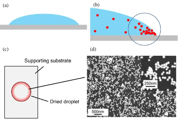
4-2-1 Dried droplet method
4-2-2 Self-assembly method by using surface modifiers 4-2-3 Interface trapping method
4-2-4 Vapor deposition method 4-2-5 Beam lithography
4-2-6 Nanosphere lithography
4-3 Guideline of fabrication of a SERS active substrate with high reproducibility and ultra-high sensitivity
4-4 Theories of colloidal nanoparticles 4-4-1 Brownian motion
4-4-2 Dewjaguin, Landau, Verwey, Overbeek (DLVO) theory
4-4-3 Lateral capillary force
4-5 A guide of fabrication of 2DMAs without any surface modifer
5 Fabrication of Two Dimensional Metal Nanoparticle Array (2DMA)
5-1 Introduction 5-2 Experimental
5-3 Results and Discussion
5-3-1 Early stage of sandwich method 5-3-2 Cleaning of supporting substrate 5-3-3 Temperature dependence
5-3-4 Features of sandwich method
5-3-5 Predictable model of sandwich method
5-4 Conclusions
9
6 Evaluation of 2DMAs with spectroscopy and chase of the assembly process
6-1 Introduction 6-2 Experimental
5-2-1 Construction of Vis-near IR microspectrometer 6-3 Results and Discussion
6-3-1 Evaluation of uniformity of 2DMAs by using SEM 6-3-2 Spectroscopic analysis of 2DMAs
6-3-3 Assembly process of the 2DMAs and its considerable mechanisms in the SW method 6-4 Conclusions
7 Surface Enhanced Raman Scattering Detection with Highly-Ordered Gold Nanoparticle Array
7-1 Introduction 7-2 Experimental
7-2-1 Preparation of SERS active substrates
7-2-2 Construction of optical system for detection of Raman scattered light
7-2-3 Sample molecule
7-2-4 Adsorption to SERS active substrates of crystal violet
7-3 Results and Discussion
7-3-1 SERS active substrates
7-3-2 SERS measurement of crystal violet molecules 7-3-3 Optimization of the dipping time
7-3-4 Enhancement factor of the 2DMA substrate
7-3-5 SERS reproducibility of each substrate
7-4 Conclusions
10
Appendix Study of two-dimensional highly-ordering of gold nanoparticles for an optical sensor by using surface plasmon excitation as an assistance effect
Introduction Experimental
Results and Discussion Conclusion
General Conclusion References
List of Publications
Acknowledgment
11
Chapter 1
General introduction
1-1 Optical functional thin film
Molecular sensor with high analytical performances such as quantitative ability, qualitative ability, label-free analysis, ultra-high sensitivity and so on is one of key technologies to make scientists’ dreams come true. It is expected that development of
this sensor leads to various applications such as medical diagnosis, biology and identification of environmental pollutant. In this stage, there are a lot of reports for development of such molecular sensors.
As one of such molecular sensors, optical functional thin films have attracted attention because these films can be easily combined with conventional spectroscopic analysis and provide us with new analytical performance via various surface effects by their photo excitation. These surface effects are divided into two types. One is surface reaction with adsorbate including photocatalytic reaction, photoisomerization and so on.
The other is unique career movement such as surface plasmon (SP) excitation, charge separation and so on. The author considered that effective utilizations of these surface effects lead to development of new molecular sensors with high analytical performance.
In this thesis, the author focused on two surface effects, photocatalytic effects
12
and surface enhanced Raman scattering, and attempted effective utilizations of these surface effect as molecular sensors by fabricating their optical functional thin films. In this chapter, these two surface effects were discussed.
1-2 Photocatalytic effect 1-2-1 Titania
Titania is white, inexpensive, non-toxic (except for nanoparticles) and chemically stable material. From these properties, titania has been used as pigment. On the other hand, photocatalytic effect of titania was discovered by A. Fujishima in 1972.
Since the discovery of photocatalytic effect of titania, titania has been studied extensively for its applications which are described in.1-2-3
Titania has three major crystal structures which include rutile, anatase and brookite. Especially, titania in anatase form is a major photocatalyst. Titania has wide band gap (3.0-3.2eV) which can absorb ultraviolet light. Photo excited titania generates electron-hole (e-h) pairs which cause photocatalytic effect.
1-2-2 Rough mechanism of photocatalytic effect
Behavior of electron-hole pairs in photo excited titania is shown below.
13
(a) Photo excitation of photocatalyst
1. Generation of e-h pairs (conduction band electrons and valence band holes).
(b) Reduction process
2. Conduction band electrons at titania surface reduce adsorbate molecules.
3. Conduction band electrons are trapped in titania surface.
4. Trapped electrons reduce adsorbate molecules.
(c) Oxidation process
5. Valence band holes at titania surface oxygenate adsorbate molecules.
6. Valence band holes are trapped in titania surface.
7. Trapped valence band oxygenate adsorbate molecules.
(d) Recombination process of e-h pairs
8. Recombination of e-h pairs with trapped e-h pairs occurs. This process does not contribute photocatalytic reaction.
Trapped e-h pairs are described in Fig. 1-1. Due to the generation of e-h pairs,
photocatalytic effects take place at the surface of titania. In fact the photocatalytic effect
is very complex because various active species such as hydroxyl radicals which
produced by reaction between holes and moisture present on the surface are produced.
14
1-3 Surface enhanced Raman Scattering (SERS) 1-3-1 Raman scattering
Raman scattering was discovered by C.V. Raman and
K. S. Krishnamin 1928 and is a type of an inelastic light scattering [1]. In this scattering process, an incident photon gains or loses its energy to interact quantized vibrational and rotational modes of an analyte molecule. In Raman spectra, these modes appear as sharp peaks and their positions depend on their transition energy, which are specific to molecular structure, along x-axis of Raman shift (cm
-1). Therefore, Raman measurement is recognized as a powerful tool for identification of analyte molecules. Analytical features of Raman scattering spectroscopy are shown below.
1. Construction of the measurement system is easy, because quartz or glass can be used as sample cell and optical devices.
2. The measurement in aqueous solution is possible, because Raman scattering cross sections of water molecules are much weaker than IR’s one and its signal don’t disturb sample’s signal.
3. Measurement in a microscopic region is possible by focusing of an excitation laser.
4. One measurement gives us much information of Raman shift in large
wavenumber region.
15
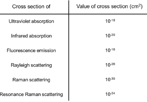
However, a general Raman spectroscopy, except for resonant Raman scattering, has a low-sensitivity compared with other spectroscopic analysis such as absorption spectroscopy, fluorescence measurement and so on. For example, typical Raman scattering cross-sections of various sample molecules are ~10
-30cm
2/molecule. In contrast, those of typical infrared absorption and fluorescence are ~10
-20and ~10
-16cm
2/molecule, respectively (table 1-1). Therefore, it is recognized that Raman measurement is limited to expand various applications such as molecular sensor due to this low-sensitivity.
Table 1-1. Typical values of cross sections for various spectroscopic measurement
16
1-2-2 History of surface enhanced Raman scattering
Fleischmann, Hendra and McQuillan reported intense vibration spectra of pyridine adsorbed on Oxidation-Reduction-cycled silver electrode in 1974 [2]. They explained that this result is caused by an increase of number of adsorbed molecules based on an increase of surface area. However, this explanation could not satisfy other researchers in fact. In 1977, both independent groups of Jeanmaire and Van Duyne [3]
and, Albrecht and Creighton [4] further examined factors which affect the huge intensity
of the Raman bands of adsorbed molecules such as surface features, potential of the
electrode, concentration of pyridine, and electrolyte composition of the solution, and
then they concluded that the intense vibration spectra of pyridine on the
Oxidation-Reduction-cycled silver electrode is caused by an enhancement of efficiency
of Raman scattering itself. This effect is known as surface enhanced Raman scattering
(SERS). Within a few years, intense Raman scattered signals based on SERS were
verified for many molecules which are adsorbed on roughened surfaces of novel metal
[5]. To this day, many researchers have been paying much attention to the huge
enhancement of Raman signals based on SERS effect for various applications, and then
a lot of studies for SERS have been reported. These studies have revealed that SERS
has major three advantages.
17
1. Sensitivity is extremely high. (Comonly, intensity of Raman scattered light is enhanced to 10
3times from 10
6times.)
2. Spatial selectivity is high, because only molecules which adsorbed on the metal surface show SERS effect.
3. Because fluorescence of adsorbed molecules is quenched, Raman scattered light can be detected without interference of large fluorescence.
1-2-3 Proposed mechanisms of SERS enhancement effect
In many papers, origin of SERS enhancement effect has been explained by two mechanisms of electromagnetic enhancement [6] and charge transfer enhancement [7-8].
Enhanced electromagnetic field generates when incident light couples with
surface plasmon (SP) phenomenon. The SP excitation is explained below. When a
specific metal surface with nano-scale roughness, such as metal nano-particles and
surface-roughened thin metal films, is irradiated with a specific wavelength laser,
almost of the laser energy is absorbed resonantly. And then great number of excited
electrons in the metal is generated and is localized on the metal surface. Therefore, these
excited electrons are densified very much and induces enormous enhanced
18
electromagnetic field in nano-space on the surface. Calculations have shown that the electromagnetic field is greatly enhanced at dislocations or sharp discontinuities on a metal surface [9, 10]. Therefore, molecules which are adsorbed on the nano-scaled surface are exposed much larger electromagnetic field than that of irradiated light. The strength of the electromagnetic field decays exponentially from the surface but the stronger electromagnetic field induces stronger Raman scattered light within several nano-meters of the surface. Especially, in the case of metal nanoparticles, when two or more particles approach each other with gap of several nanometers, the shorter gap distance produces larger enhanced electromagnetic field in “hot site” between the particles, which reaches to more than 10
10times [11]. However, when this gap distance is zero, the enhancement factor of electromagnetic field significantly reduces.
In the charge-transfer enhancement mechanism, analyte molecules are bound to the metal surface to form charge transfer complexes. The incident light excites electrons in the metal and the excited electrons play a role of carrier of energy transfer to the analyte through generated new adsorption state between metal surface and sample molecules. In other words, this process is similar to that in resonant Raman scattering.
It is generally recognized that the electromagnetic enhancement factor is much
larger than the charge transfer enhancement factor. Main steps of SERS mechanism
19
based on the theory of the electromagnetic enhancement effect are as follows [12]:
(1) An analyte molecule adsorbs on a nanostructured metal surface so that incident light couples with surface plasmon.
(2) Energy from the surface plasmon transfers to the adsorbed analyte and the Raman process occurs on the molecule, as shown in Fig. 1-1 (a).
(3) Energy transfers back to the plasmon, as shown in Fig. 1-1 (b).
1-2-4 SERS active substrates
As described above, activity of SERS effect requires nano-structured metal
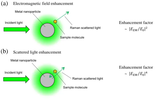
Fig. 1-1. Schematic illustration of SERS mechanism based on electromagnetic enhancement
(a)
(b)
Electromagnetic field enhancement
Enhancement factor
~
𝐸𝐸𝑀 𝐸0 2Scattered light enhancement
Enhancement factor
~
𝐸𝐸𝑀 𝐸0 420
surface. A substrate of metal with nano-sized surface roughness is called a SERS active substrate. Designing of a SERS active substrate is essential for high performance SERS measurement, because intensity and reproducibility in SERS measurement mainly depend on the surface structure of SERS active substrate such as morphology, uniformity and so on. Especially, inexpensive high-throughput fabrication of SERS active substrates with high reproducibility and large enhancement effect is a prerequisite for sensor applications.
General types of SERS-active substrates exhibiting enhancement effect are
assembly of colloidal metal nanoparticles in the 10-150 nm size range, vapor-deposited
films and electrodes of these metals [13]. As well as these substrates, many groups have
been developing new techniques for making nanoparticles [14-23], nanoshells [24-27],
nanosphere formed by nanosphere lithography [28-31], nanogaps [32-33], nanowire
[34-35], and nanoholes [36-37]. For the most part of these substrates, gold or silver have
been used as a material of SP excitation for making SERS substrates, although other
materials such as aluminum [38], indium [39], copper [40], and gallium [41] can also
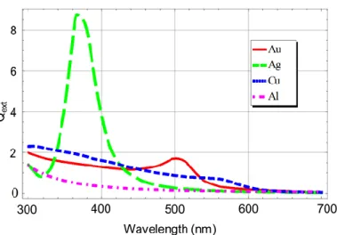
support SP resonances in the UV-VIS-NIR range. Efficiencies of SP excitation typical
metal are shown in Fig. 1-2 [42]. The reason why gold and silver are used mainly for
SERS substrates is as follows; gold is a high chemical stability with higher efficiency of
21
SP excitation than that of various metals except silver. On the other hand, silver has the highest efficiency of SP excitation in various metals, although silver has a low chemical stability.
1-2-5 Quantitative analysis using SERS
SERS almost has not been applied for practical uses as molecular sensors, although there are a lot of studies. The major reason is that conventional SERS has too poor quantitative performance to apply for various practical uses. This poor quantitative performance is caused by non-uniform surfaces of conventional SERS active substrates, because a magnitude of electromagnetic enhancement effect on the surface of SERS active substrate strongly depends on its morphology. Therefore, in order to apply SERS
Fig. 1-2. Extinction coefficient as a function of wavelength for a metal nanoparticle (diameter: 60nm) in air. These spectra were calculated by using Mie theory by reference to [42].
22
active substrates to a quantitative analysis, control of the enhancement effect is required.
In other words, uniform surface roughness of nanostructure is required.
Vapor-deposited films and electrodes of these metals have too random surface
roughness to control their surface roughness. Therefore, the author focused on metal
nanoparticles with same shape and size. When metal nanoparticles are used as a SERS
active substrate, optical properties of single metal particle have to be well controlled,
that is, metal nanoparticles must not become aggregations. In the case of assembly of
particles, inter-particle distance between metal nanoparticles is a very important factor
because very short distance below several nano-meters generates “hot site” with a huge
enhancement effect at the nano-space between metal nanoparticels. For quantitative
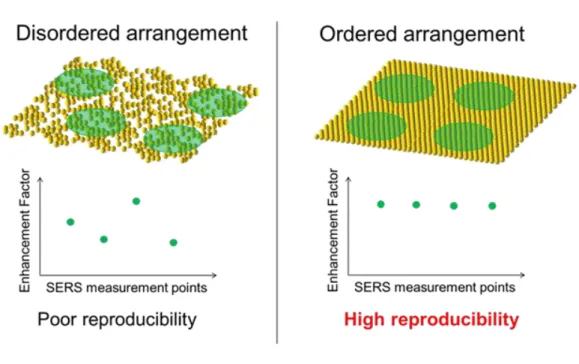
analysis, a number of the “hot site” in measurement area should be controlled, as shown
in Fig. 1-3. However, fabrication of such uniform surface roughness of nanostructure
including “hot sites” is very difficult, because metal nanoparticles are easily to
aggregate due to their strong attractive force based on van der Waals force.
23
1-3 Purpose
In this thesis, the author aims for fabrication of two types of optical functional thin films for development of molecular sensors with high analytical performance.
Firstly, the author aims for improvement of analytical performance of surface assisted laser desorption/ionization mass spectrometry (SALDI-MS) described in Chapter 2 by using titania thin films which cause photocatalytic reactions. Commonly, mass spectrometry combined with soft ionization methods such as matrix assisted LDI-MS (MALDI-MS) and SALDI-MS provide us with molecular-weight of analyte
Fig. 1-3. Schematic illustration of relationship between arrangement of metal
nanoparticles and reproducibility.
24
molecule. However, only information of molecular-weight is not enough to identify molecular structures which have many structural isomers such as sugar chains and so on.
In order to identify their molecular structures, the author considered that a selective fragmentation in MS measurement is effective because site selective fragmented ions have structural information of analyte molecules. Therefore, the author paid attention to photocatalytic degradations of adsorbate molecules. In this thesis, the author fabricates titania thin films as SALDI-MS substrate and investigates relationship between titania SALDI spectra pattern and photocatalytic effect.
Secondly, the author aims for fabricating a SERS active substrate which enables to analyze quantitatively. The author considered that a nanostructured surface of the SERS active substrate should be composed by same metal nanoparticles in order to generate uniform electromagnetic enhancement field on all region of the substrate.
Therefore, the author focused on highly-ordered two-dimensional metal nanoparticle array (2DMA).
However, conventional 2DMA substrates fabricated by several methods have
two major drawbacks in terms of SERS sensor. One 2DMAs substrate needs surface
modifiers which are usually used to prevent metal nanoparticles from aggregating due to
its steric repulsion. In this case, these surface modifiers give us negative effects and are
25
described in chapter 3. Another one without using any surface modifiers has low uniformity in the fabricated 2DMA. These problems are discussed in Chapter 3 in detail.
On the other hand, our group succeeded in fabrication of highly-ordered 2DMA without any surface modifier by using the novel technique, which is called sandwich (SW) method. However, the 2DMA could not work for SERS analysis. The reason was that an area of the 2DMA was too small (<mm
2) to obtain many SERS spectra from one substrate and to estimate the quantitative performance, although its SERS enhancement is enough large. In this thesis, the author optimized the fabrication condition of the SW method in order to expand the area of the 2DMA, and chased a fabrication mechanism in the SW-method, simultaneously. And, the author applied the 2DMA to SERS measurement with high reproducibility.
In chapter 2, SALDI-MS measurements of oligosaccharides on the titania substrate, which were prepared by using oil/water interface trapping method, were discussed. And then the relationship between titania SALDI-MS spectra pattern and photocatalytic effect was discussed.
In chapter 3, fundamentals of localized SP (LSP), calculation of optical
26
properties of gold nanoparticles (AuNPs) and inter-particle coupling effect are discussed in order to understand a relationship between LSP and electromagnetic enhancement in SERS.
In chapter 4, common fabrication methods of two-dimensional metal nanostructure and the reason why the author paid attention to 2DMAs as quantitative SERS active substrates are discussed. And, the theory for interactions between colloids in solution is discussed.
In chapter 5, the fabrication method (SW-method) of 2DMAs without any surface modifier and characterization of the 2DMA using scanning electron microscope with Fourier transform analysis are discussed.
In chapter 6, mechanism of SW-method was discussed by using Vis adsorption spectroscopy and optical microscope.
In chapter 7, an analytical performance such as reproducibility and
quantitatively of SW-substrate in SERS measurement is discussed.
27
Chapter 2
Titania surface assisted laser desorption/ionization mass spectrometry of oligosaccharides
2-1 Introduction
Laser desorption ionization (LDI) mass spectrometry (MS) was reported in the 1960’s. In LDI-MS, sample molecules directly receive enough energy to desorb/ ionize from excitation laser. Detected ion species are mainly M
+and their fragment ions.
LDI-MS is appropriate for low molecular weight organic compounds which can absorb a laser. On the other hand, LDI-MS is not suitable for identification of nonvolatile compounds such as biological molecules and polymers because direct laser irradiation to such compounds cause fragmentation drastically. Thus, LDI-MS had not been paid attention until the development of matrix-assisted LDI-MS.
The matrix-assisted LDI (MALDI) was developed by K. Tanaka [43], who received the 2002 Nobel Prize in Chemistry, and F. Hillenkamp [44]. Because MALDI-MS had been improved remarkably in fragmentation of analytes with conventional LDI-MS, the use of the MALDI-MS has spread rapidly all over the world as a very effective analysis method.
In MALDI-MS, samples are prepared by mixing analytes and excessive
28
amounts of matrix molecules which can absorb a laser. Matrix molecules have three major roles to measure with high analytical performance. The first is that matrix molecules transfer absorbed photon energy from an exciting laser to surrounding analytes. In other words, matrix molecules assume a role of energy mediator. As a result, MALDI-MS measurement can avoid laser absorption of analyte. The second is that analytes which have strong intermolecular interactions are dispersed by matrix molecules. The third is that these molecules become a proton [H]
+source to ionize sample molecules as [M+H]
+. From these reasons, MALDI-MS can identify high molecular-weight and nonvolatile compounds such as biological molecules and polymers with less fragmentation.
However, some drawbacks related to analytical performance exist. First, the
mixture of analyte and excessive amounts of matrix molecules has large heterogeneities
of not only concentration but also morphology. These heterogeneities cause too low
reproducibility to analyze quantitatively. Second, LDI process produces many peaks of
matrix molecules including their fragment ions and multimer. These peaks interfere
with identification of low molecular-weight compounds. To overcome such drawbacks,
many attempts have been made so far including use of additive such as ammonium salts,
serine and cyclodextrines.
29
Surface-assisted LDI (SALDI) -MS is expected as one of alternative techniques
for resolution of above-mentioned problem [45-47]. In the SALDI-MS, surface of
inorganic material as an ionization substrate absorbs laser energy and supplies enough
energy to desorb/ionize analytes on the surface. However, concerning practical utility,
the remarkably lower sensitivity of the most SALDI-MS method compared to that of the
MALDI-MS method, except in a few reports of SALDI-MS methods [45], is more
serious than the abovementioned negative effect. The remarkably low sensitivity may be
caused by the assumption that the ionization mechanisms in the SALDI methods are
similar to the ionization mechanisms mainly based on rapid thermal energy supply in
the MALDI method. In recent years, research on the nano-roughened surface has been
progressing dramatically. Hence, their surface properties have been applied to
SALDI-MS measurement for improvement the analytical performance such as
sensitivity, selectivity and more. For example, Kawasaki and co-workers reported
selective detection of peptides by using sulfonate group-modified FePtCu nanoparticles
surface as a SALDI-MS substrate [46]. Sato and co-workers discussed interaction
between surface property and SALDI-MS signal intensity by using pyroelectric
substrate as a SALDI-MS substrate [47]. The author should consider that these SALDI
substrates give not only thermal energy but also some surface effects from their surface
30
to sample molecules.
Currently, we have succeeded in detection of ultratrace samples by utilizing localized surface plasmon excitation on AuNPs surface [48]. It is understood that AuNPs can effectively absorb laser energy in the specific wavelength region via localized surface plasmon excitation, and cause charge interaction between the surface and adsorbed molecules. The author considered that the photo-excited surface may become an important key for a new application of SALDI-MS method. In this study, the author focused on a titania surface as a SALDI-MS substrate because photo-excited titania has a unique surface property based on electron-hole pairs which can cause interesting phenomena called photocatalytic reactions.
2-2 Experimental
Titania nanoparticles (Degussa, P 25) were purchased from Nippon aerosil.
P25 (anatase: rutile = 3:1, average particle diameter: 30 nm) is known as a conventional
photocatalytic material, which has a relatively large surface area (49 m
2/g) [49]. Titania
thin films as ionization substrates were formed on n-type Si (100) (purchased from
Nilaco) using a film formation method at a liquid-liquid interface (titania
suspensiontoluene). For comparison, silicon substrates with comparable roughness to
31
the titania substrates were prepared with a sandpaper. As sample molecules, the author selected oligosaccharides, such as
-cyclodextrin (-CD; purchased from Wako) andtetra-N-acetylchitotetraose, because these samples have no absorbance for an excitation laser. Each sample molecule was solved in ion-exchanged water (1 mmol/l) without a cationization salt. Each sample solution (ca. 1 μL, amount of sample molecules: 1nmol) was dropped on the titania thin film substrate, and then were dried at room temperature in dark room. These substrates were put into a linear time-of-flight mass spectrometer made by our laboratory with delayed extraction ion source. Acceleration voltage was 4.0kV-3.0kV and mass spectra were obtained by the positive ion mode. Nd:YAG pulsed laser FHG (λ =266 nm, 8 ns pulse width, a 10 Hz frequency) was used as an excitation
laser. The laser beam was focused onto the surface with optical lens and its spot diameter was set to 0.17 mm. Its laser fluence was set to slightly stronger power (15 μJ/pulse) than thresholds for ionization of sample molecules.
-cyclodextrin(-cd)
tetra-N-acetylchitotetraose
Fig. 2-1. Structural formulas of sample molecules.
32
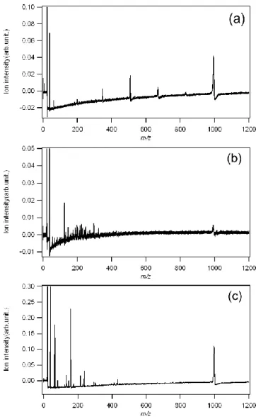
2-3 Results and Discussion
Fig. 2-2 (a) shows mass spectra of -CD measured by our method (without any cationization agents). [-CD+Na]+ was detected strongly at m/z = 995, and several kinds of ions were detected at m/z = 349, 511, 673 and 835. The author considered that these ions come from -CD because these ions were not detected on titania SALDI-MS
substrate without
-CD. Differences in m/z values between these fragment ions weremultiples of 162 Da. Because component monosaccharide of
-CD is D-glucose withFig. 2-2
(a) Mass spectra of a-CD
measured by using a titania SALDI-MS substrate without citric acid.
(b) Mass spectra of a-CD
measured by using surface roughened silicon substrate without citric acid.
(c) Mass spectra of a-CD
mesured by using a titania SALDI-MS
substrate with citric acid.
33
m/z value of 180 Da, -CD is combination of dewatered D-glucose with m/z of 162 Da.
This decrease of 162 Da agrees with decrease of number of suger units. From this reason, the author considered that these fragment ions were generated by dissociation of
-CD. However, m/z values of Na adduct biose, triose, tetraose and pentaose are 365,
527, 689 and 851, respectively, these m/z values were 16 Da higher than those of detectied ions. These differences of m/z values of 16 Da are very unique because these fragment ions were not observed by conventional LDI-MS measurement. At this stage, the author thinks that this value of 16 Da may correspond to oxygen atom in glycoside bond, although the author has no critical evidences.
In order to verify this unique result, the author attempted same SALDI-MS measurement by using surface roughened silicon substrate, as shown in Fig. 2-2 (b). In Fig. 2-2 (b), these unique fragment ions of
-CD cannot be detected with any laserfluence, although a [-CD+Na]
+signal and many signals in low mass region from m/z =
150 to 350 were observed. Moreover, not only other SALDI-MS substrate such as metal
nanoparticle thin film but also other excitation laser wavelengths such as 532 nm and
1064 nm gave us similar spectral pattern to this silicon substrate. It is known that these
many signals in low mass region are caused by thermal dissociation. From these
measurements, the author considered that these unique fragment ions on titania
34
SALDI-MS substrate are not caused by thermal dissociation. In order to investigate the mechanism of the non-thermal fragmentation, the author added typical cationization agent of sodium citrate (1nmol) to -CD on titania SALDI-MS substrate, as shown in
Fig. 2-2 (c), because sodium citrate is reported as a hole scavenger [50]. In Fig. 2-2 (c), detected ions were not these unique fragment ions but non-dissociated ions and thermal dissociated ions. This result shows that sodium citrate may lose charge interaction based on e-h pairs which is one of surface property of titania. For more verification, the author measured tetra-N-acetylchitotetraose (N-AT) by using titania SALDI-MS substrate without any cationization agent, as shown in Fig. 2-3. N-AT has component monosaccharide with m/z value of 221Da and is combination of dewatered monosaccharide with m/z value of 203Da. As well as Fig. 2-2 (a), [N-AT + Na]
+, [triose-16+Na]
+and [biose-16+Na]
+were detected at m/z = 853, 611 and 431, respectively. These results show that titania SALDI-MS substrate causes unique dissociation of oligosaccharide.
Fig. 2-3.
Mass spectra of N-AT Measured by using
titania SALDI-MS substrate without citric acid
35
In summary, SALDI-MS measurements of oligosaccharides on the titania
substrate, which were prepared by using oil/water interface trapping method, were
discussed. A lot of fragment ions of oligosaccharides were observed. These fragment
ions had periodical molecular weight which is correspond to oligosaccharide units only
by our substrate. It is suggested that the unique fragmentation process on the titania
SALDI-MS substrate relates to photocatalytic reaction. Moreover, the author thinks that
the unique fragmentation may be are useful to structural analysis of oligosaccharides
because the titania SALDI-MS have a selective fragmentation to glycoside bonds.
36
Chapter 3
Localized Surface Plasmon Resonance (LSPR)
In chapter 1, the author had already described that an electromagnetic field caused by localized surface plasmon resonance (LSPR) is a dominant enhancement factor in SERS mechanisms. In this chapter, LSPR is discussed in detail in order to obtain a guideline for fabrication of a SERS active substrate with a high reproducibility and an ultra-high sensitivity.
3-1 What is LSPR?
Metal nanoparticles with a size (several tens of nanometers) much smaller than
a wavelength of light exhibit brilliant colors. These colors are quite different from a
bulk metal and so have attracted much interest of people. For example, AuNPs and
silver NP have wine red and yellow color, respectively. And, the brilliant colors were
employed in stand-glass manufacture in the middle ages. The origin of the brilliant color
is attributed to strong absorption of incident light in a specific wavelength region and
scattering of incident light by metal nanoparticles dispersed in medium [51-52]. And,
the origin of the strong absorption is attributed to a resonance of collective oscillation of
conduction electrons with incident electromagnetic radiation [53-54]. This collective
37
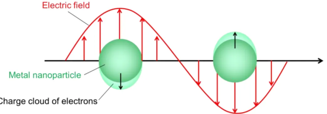
oscillation of free electrons in the metal is called a LSPR.
Plasma is described as an electrically neutral medium where an electron, ion, or its both can move freely. Since metal contains many free electrons, it can be considered to be a kind of plasma. In 1952, Pines and Bohm suggested an existence of plasma oscillation of electrons in a metallic solid to explain energy losses of fast electrons passing through metal foils [55]. This excitation is called plsmon polariton. Especially, when a surface exists, the plasma oscillation at the surface is different from that in bulk metal, as shown in Fig. 3-1. This excitation is called a surface plsmon (SP) polariton.
Generally, for simplicity, the word of the polariton is often omitted.
SP associated with a metallic film whose thickness is several tens nanometers can travel across the interface between with the film and a dielectric. A type of this SP is called a propagating SP. On the other hand, SP associated with metal nanoparticles with
Fig. 3-1. The origin of localized surface plasmon resonance in nanoparticle
38
a size of several tens of nanometers is called a LSP. The LSPR caused by a coupling between electrons and incident photon in a frequency of oscillation can be characterized as a strong absorption band [56-57].
3-2 Relationship between electromagnetic filed caused by LSPR and SERS intensity
The SERS effect is a direct correspondence with the LSPR producing an intense electromagnetic field on the SERS active substrate. SERS is a phenomenon associated with the enhancement of the electromagnetic field surrounding a metal object optically excited near an intense dipole (or multipole) resonance. The radiated dipolar fields excite adsorbed molecules, and if the resulting molecular radiation remains at resonance with the enhancing object, the scattered radiation will again be enhanced.
Therefore, under appropriate circumstances, an influence that the electromagnetic enhancement gives in SERS intensity can be explained as a following formula;
I(𝜔2) = 𝑁𝐴 𝐿(𝜔1) 2 𝐿(𝜔2) 2𝐼𝑖𝑛(𝜔1)
where
I(𝜔2), N, A, 𝐿(𝜔1), 𝐿(𝜔2) and 𝐼𝑖𝑛(𝜔1) are intensity of enhanced Ramanscattered light, the number of molecules involved in the SERS process, Raman cross
section of the molecule in contact with the surface of SERS active substrate, localized
39
field factor (enhancement factor of electromagnetic field) of excitation light, localized field factor of Raman scattered light and intensity of an electromagnetic field of the incident light, respectively. If enhancement factor of excitation light is as large as enhancement factor of Raman scattered light, intensity of enhanced Raman scattered light is proportional to the fourth power of the electromagnetic enhancement. Therefore, the electromagnetic enhancement based on LSPR is important for development of sensitive SERS-active substrate, and to understand the electromagnetic enhancement, optical properties of metal nanoparticles should be understood.
3-3 Dielectric functions of metal nanoparticle
Gold and silver NPs are commonly studied because they can exhibit strong LSP in the ultra violet and visible region. In this region, their optical properties can be described by a wavelength-dependent dielectric function
(𝜀). The dielectric function (𝜀) is important in order to calculate optical and plasmonic property. Values of thedielectric function are complex numbers (
ε = ε′+ iε′′). Values of the complex
dielectric function of bulk gold at different wavelength were obtained from Johnson and
Christy [58]. And then, the dielectric function corrected for nanoparticle size (ε(𝜔)) by
using following formulas.
40
ε(𝜔) = 𝜀𝑏𝑢𝑙𝑘(𝜔) + 𝜔𝑝2
𝜔2+ 𝑖Γ𝑏𝑢𝑙𝑘𝜔− 𝜔𝑝2 𝜔2 + 𝑖Γ𝜔 Γ = Γ𝑏𝑢𝑙𝑘 +𝑣𝐹
𝑟1
𝜀𝑏𝑢𝑙𝑘(𝜔) is the dielectric function of bulk gold. 𝜔, 𝜔𝑝
,
Γ, Γ𝑏𝑢𝑙𝑘,
𝑣𝐹and
𝑟1are
frequency, plasma frequency of gold (13.8×10
15s
-1), damping constant of AuNP, damping constant of bulk gold (1.08×10
14s
-1), Fermi velocity (1.39×10
8cm s
-1) and radius of a AuNP, respectively. Water as surrounding medium for AuNPs with a dielectric function
𝜀2was calculated a following formula reported by Thormahlen [59].
ε(λ) =5.743534 × 10⁻³
𝜆2− 0.018085 + 1.769238 − 2.797222 × 10⁻²× 𝜆2+ 8.715348 × 10⁻³
× 𝜆4− 1.413942 × 10⁻³× 𝜆6
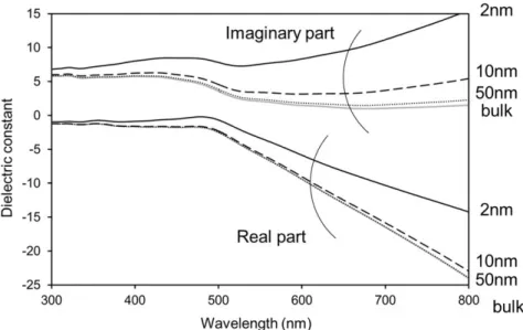
Obtained these dielectric functions were shown in Fig. 3-2, 3-3. In future calculations, it was calculated using the values.
Fig. 3-2. Dielectric functions of spherical AuNPs
41
3-4 Quasistatic approximation
A quasistatic approximation is simple and gives good results when a diameter of particle is much smaller than the wavelength of the incident light, although this theory is classical. In this thesis, the author tried to evaluate optical properties of nanosphere by using the quasistatic approximation because the author treated with only nanosphere.
In the quasistatistic approximation, the Laplace equation for the scalar potential,
Φ, can be solved.∇2Ψ = 0
(An electric field, E, is given by the gradient of the scalar potensial,
E = −∇Ψ.)This formula can be represented in spherical coordinates.
1 𝑟2
𝜕
𝜕𝑟(𝑟2𝜕Ψ
𝜕𝑟) + 1 𝑟2sin 𝜃
𝜕
𝜕𝜃(sin 𝜃𝜕Ψ
𝜕𝜃) + 1 𝑟2sin2𝜃
𝜕2Ψ
𝜕𝜙2 = 0
Fig. 3-3. Dielectric function of water
42
Here,
Ψ is set as follows.Ψ = R(𝑟)Θ(𝜃)Φ(𝜙) 1
𝑅 𝑑
𝑑𝑟(𝑟2𝑑𝑅
𝑑𝑟) = 𝑛(𝑛 + 1) sinθ
Θ 𝑑
𝑑𝜃(sin𝜃𝑑Θ
𝑑𝜃) = 𝑚2− 𝑛(𝑛 + 1)sin2𝜃 1
Φ 𝑑2Φ
𝑑𝜙2 = −𝑚2
The solution of these equations is expressed as follows.
R = 𝐴𝑛𝑟𝑛+ 𝐵𝑛 1 𝑟𝑛+1
Θ = 𝐶𝑚𝑛𝑃𝑛𝑚(𝑐𝑜𝑠𝜃) + 𝐷𝑚𝑛𝑄𝑛𝑚(𝑐𝑜𝑠𝜃) Φ = 𝐸𝑚exp(𝑖𝑚𝜙) + 𝐹𝑚exp (−𝑖𝑚𝜙)
(𝑃
𝑛𝑚and
𝑄𝑛𝑚are Legendre functions.)
When
𝜃 equal 0, 𝑄𝑛𝑚(𝑐𝑜𝑠𝜃) diverge. Therefore, Ψ is given as follow.Ψ = ∑∞𝑛=0∑∞𝑚=0(𝑎𝑛𝑟𝑛+ 𝑏𝑛𝑟𝑛+11 )𝐶𝑚𝑛𝑃𝑛𝑚(𝑐𝑜𝑠𝜃)( 𝐸𝑚exp(𝑖𝑚𝜙) + 𝐹𝑚exp (−𝑖𝑚𝜙))
When an incident electric field is symmetric for z-axis, the term of φ does not exist, and only a term of m=0 remains.
Ψ = ∑ (𝑎𝑛𝑟𝑛 + 𝑏𝑛 𝑟𝑛+1)
∞
𝑛=0 𝑃𝑛0(𝑐𝑜𝑠𝜃)
Moreover, when an incident electric field is plane wave incidence for the z-axis, incidence potential
Ψ0can be described as follow.
Ψ0 = −𝐸0𝑧 = −𝐸0𝑟𝑐𝑜𝑠𝜃 = −𝐸0𝑟𝑃10(𝑐𝑜𝑠𝜃)
43
From boundary condition, only a term of n=1 remains.
Ψ = (𝑎𝑟 + 𝑏
𝑟2) (𝑐𝑜𝑠𝜃)
An internal potential (Ψ
1) of the sphere and an outside potential (Ψ2 = Ψ0+ Ψ𝑠𝑐𝑎) ofthe sphere satisfy boundary conditions on the surface of the sphere.
Ψ𝑠𝑐𝑎is scattering potential. If
𝑟1equals radii of the sphere, boundary condition of electric field and electric flux density are expressed as follows.
∂Ψ1
∂θ 𝑟=𝑟1 =∂Ψ2
∂θ 𝑟=𝑟1 𝜀1∂Ψ1
∂r 𝑟=𝑟1 = 𝜀2∂Ψ2
∂r 𝑟=𝑟1
(𝜀
1: dielectric function of the sphere, 𝜀2: dielectric function of medium.)
When above differential equations are solved,
Ψ1and
Ψ2are expressed as follows.
Ψ1 = − 3𝜀2
𝜀1+ 2𝜀2𝐸0𝑟𝑐𝑜𝑠𝜃 Ψ2 = −𝐸0𝑟𝑐𝑜𝑠𝜃 + 𝜀1− 𝜀2
𝜀1+ 2𝜀2𝑟13𝐸0𝑐𝑜𝑠𝜃 𝑟2
Electric field is explained by
E = −grad Ψ.𝐸1 = 3𝜀2
𝜀1+ 2𝜀2(𝐸0𝑐𝑜𝑠𝜃𝑒𝑟− 𝐸0𝑠𝑖𝑛𝜃𝑒𝜃) = 3𝜀2
𝜀1+ 2𝜀2𝐸0𝑒𝑧 𝐸2 = 𝐸0𝑐𝑜𝑠𝜃𝑒𝑟− 𝐸0𝑠𝑖𝑛𝜃𝑒𝜃+ 𝜀1− 𝜀2
𝜀1+ 2𝜀2 𝑟13
𝑟3𝐸0(2𝑐𝑜𝑠𝜃𝑒𝑟+ 𝑠𝑖𝑛𝜃𝑒𝜃)
= 𝐸0𝑒𝑧+ 𝜀1− 𝜀2 𝜀1+ 2𝜀2
𝑟13
𝑟3𝐸0(2𝑐𝑜𝑠𝜃𝑒𝑟+ 𝑠𝑖𝑛𝜃𝑒𝜃)
(𝑒
𝑧, 𝑒𝑟, 𝑒𝜃are unit vectors)
44
This electric field is equal with the place that is generated when electric dipole moment p to be given in the next expression was put in the center of the sphere.
p = 𝜀2𝛼𝐸0 α = 4π𝑟13 𝜀1− 𝜀2
𝜀1+ 2𝜀2
Therefore, we can consider the sphere in an electrostatic field to be one electric dipole put in the center. According to these formulas, when Re (𝜀
1+ 2𝜀2) equals zero, thevalue of
α becomes very large, and this state is LSPR.3-4-1 Scattering cross-section and absorption cross-section
As a guideline of characterizing optics properties of nanoparticles, a scattering
cross section and an absorption cross section are used well. A scattering cross section is
a cross section of the incident planar wave to equal all power of the scattered light. An
absorption cross section is a similar definition. Moreover, an extinction cross section is
a sum of a scattering cross section and an absorption cross section. These are explained
as following formulas. In these calculations, a formula of polarizability which is
corrected for nanoparticle size was used, because an above-mentioned formula of
polarizability lacks a precision to obtain these cross sections. In this thesis, the author
didn’t use the above-mention formula but a formula corrected for a size of
nano-particles calculation of polarizability.
45
Scattering cross-section:
𝐶𝑠𝑐𝑎= 𝑘6𝜋4 𝛼 2Absorption cross-section:
𝐶𝑎𝑏𝑠 = 𝑘 𝐼𝑚(𝛼)Extinction cross-section:
𝐶𝑒𝑥𝑡 = 𝐶𝑠𝑐𝑎+ 𝐶𝑎𝑏𝑠α: polarizability (corrected for nanoparticlesize [60]):
α = 4π𝑟13 (𝜀1− 𝜀2) (1 − 𝑞10)2
(𝜀1+ 2𝜀2) − [ 710 𝜀1− 𝜀2] 𝑞2− (𝜀1− 𝜀2)𝑖 23𝑞3
𝜀1: dielectric function of a AuNP
𝜀2: dielectric function of surrounding medium such as air, water and more q =2𝜋𝑟1
𝜆 (𝑞: 𝑠𝑖𝑧𝑒 𝑝𝑎𝑟𝑎𝑚𝑒𝑡𝑒𝑟)
3-4-2 Calculation of optical properties of gold nanospheres
Figure 3-4 (a) and (b) show calculated spectra of the absorption and scattering
cross-sections for spherical AuNPs (diameter: 20, 60 and 100nm) normalized by its
volume in water.
46
Strong peaks due to LSPR were observed from 500nm to 600nm on both spectra of the scattering cross-section and the absorption cross section. Shorter diameter gave us lower values of scattering cross section. This tendency is caused by a larger value of an imaginary part of dielectric constant for smaller diameter of the nanoparticle. On the other hand, a larger diameter of the nanoparticle gave us a larger shift of the strong peak.
It is considered that this red shift is caused by an increase of mean free path of electrons excited by LSP in the particle.
Fig. 3-4. (a) Scattering cross-sections normalized by volume of spherical AuNPs
(diameter: 20, 60, 100nm) (b) Absorption cross-sections normalized by volume of
spherical AuNPs (diameter: 20, 60, 100nm)
47
Next, to evaluate the validity of the calculation, the author compared the result of calculation with experimental value. Dotted line in figure 3-5 (a) is a measurement data of an absorption spectrum of AuNP (diameter: 60nm) colloidal solution.
The calculated spectrum and the experimental spectrum were almost in agreement, although there were a slight difference (𝜆
𝑚𝑎𝑥of calculated spectrum: 529nm,
𝜆𝑚𝑎𝑥of experimental spectrum: 536nm) in a wavelength of maximum absorption between these two spectra. This slight difference may be caused by (A) change of the dielectric constant of material by existence of an electrolyte or (B) retardation effect (dipole → quadrupole; described in Fig. 3-5 (b)) of phase in the nanoparticle. However, the author selected this calculation method for behavior of LSP in an absorption spectrum because Fig. 3-5 (a). (solid line) Extinction cross-sections normalized by volume of spherical AuNPs (diameter: 60nm) (dotted line) A measurement data of an absorption spectrum of AuNP (diameter: 60nm) colloidal solution. (b). An image of retardation effect
(a) (b)
48
![Fig. 4-6. Schematic illustration of nanosphere lithography Amanda J. Haes et al. MRS Bulletin vol 30 2005 [85]](https://thumb-ap.123doks.com/thumbv2/123deta/10115814.1949793/63.892.198.683.381.702/fig-schematic-illustration-nanosphere-lithography-amanda-haes-bulletin.webp)