Integration for Non-Isolated
DC-DC Converters
September 2016
Wilmar Hernan Martinez Martinez
Interdisciplinary Graduate School
of Science and Engineering
To:
My Family and Diana
Abstract
Electric Vehicle (EV) applications are an improved, alternative and emerging technology that is causing a growing interest due to the reduced fuel consumption if offers and the benefits it brings to issues like greenhouse emissions in transportation systems. These vehicles have a long way to go in terms of technological improvements. They demand high efficient, compact and high-power converters in order to supply the enough torque and the needed speed in the daily requirements of the users. These requirements become critical especially in places with varying topography and unstable soils.
Nevertheless, high efficient, high power density and high voltage gain operation are required in the DC-DC converter that interfaces the storage unit with the electric motor and in the DC-DC converter between the storage unit and the auxiliary systems. These features allow to keep the power and autonomy of the electric propulsion system and to have an efficient use of the energy from the storage unit.
In this context, interleaving phases and magnetic integration are known as effective techniques to reduce the volume and mass of power converters as well as the probable increase of the converter efficiency. Therefore, this thesis presents a detailed analysis of several applications of magnetic integration for non-isolated DC-DC converters for these applications.
First, the total volume analysis of the two-phase interleaved boost converter with three different magnetic components is proposed. As part of this analysis, novel magnetic integration techniques and a novel technique to increase the reduce fringing losses are proposed to increase the power density and the efficiency of these converters. From this analysis, the power density is evaluated from the electric and magnetic modeling.
Second, the magnetic integration technique is evaluated in the proposed single-phase and two-phase tapped-inductor converters with saturable-inductors in order to reduce the recovery phenomenon on the main diodes. These topologies are proposed and evaluated in order to obtain a high efficiency in DC-DC conversion.
Third, for auxiliary systems where low voltage is required to feed non-propulsive load, a high step-down DC-DC converter is proposed to supply these low-voltage loads by a high voltage power supply. Therefore, a high-step-down converter with integrated winding-coupled inductor offers the advantage of a high conversion ratio keeping a high power density and a suitable efficiency. This converter is evaluated and compared with other outstanding high step-down converters.
Finally, a High Step-Up DC-DC converter is proposed as a solution for EV applications where the storage unit voltage is much lower than the voltage required by the motor. This novel converter uses the well-known technique of coupling inductors for achieving high power density and high voltage-gain. This converter is studied in detail, compare to other outstanding converters, and evaluated. Moreover, a parasitic analysis is conducted in order to evidence the advantages of the proposed converter.
In summary, the magnetic integration technique is studied and evaluated in detail for several DC-DC converter topologies, some of them proposed by the author. These analyses include electric and magnetic modeling, characterization of power devices, thermal analysis, geometry analysis, and electric and magnetic design. Moreover, all the presented analyses are validated with experimental tests and some of them with Finite Elements Modeling.
Conclusively, magnetic integration technique proved to be an effective technique with outstanding advantages that can be used in EV applications for increasing the power density, the conversion efficiency, and the voltage gain.
Keywords: DC-DC Converters; Magnetic Integration; Interleaved Converters; Coupled Inductor; Efficiency; Power Density; High Voltage Gain; Electric Vehicles.
Table of Contents
Abstract ... V Table of Contents ... VII List of Figures ... XI List of Tables ... XV
1. Introduction ... 1
1.1 Power electronics in Renewable Energies and Electric Vehicle applications ... 1
1.2 Isolated and Non-Isolated converters ... 2
1.3 Multi-phase and magnetic integration in Non-Isolated converters ... 3
1.4 Outline of the thesis ... 4
References ... 5
2. Two-Phase Interleaved Boost Converter ... 9
2.1 Introduction ... 9 2.2 Inductor Sizing ... 11 2.2.1 Core size ...11 2.2.2 Core losses ...12 2.2.3 Winding size ...12 2.2.4 Winding losses ...13 2.3 Inductor Modeling ... 13
2.3.1 Single phase converter ...14
2.3.2 Interleaved converter with non-coupled inductors ...14
2.3.3 LCI converter ...15
2.3.4 IWCI converter ...15
2.3.5 Volume and losses comparison ...16
2.4 Cooling Devices Volume ... 17
2.4.1 Semiconductor losses ...17
2.4.2 Heat sink modeling ...18
2.5 Volume Comparison ... 20
2.5.1 Power devices ...20
2.5.2 Total volume ...21
2.6 Inductor Size Evaluation ... 22
2.7 Experimental Results of the Volume Comparison ... 23
2.7.1 Inductors ...23
2.7.2 Power devices ...24
2.7.4 Capacitors ... 24
2.7.5 Volume evaluation ... 25
2.7.6 Experimental results ... 26
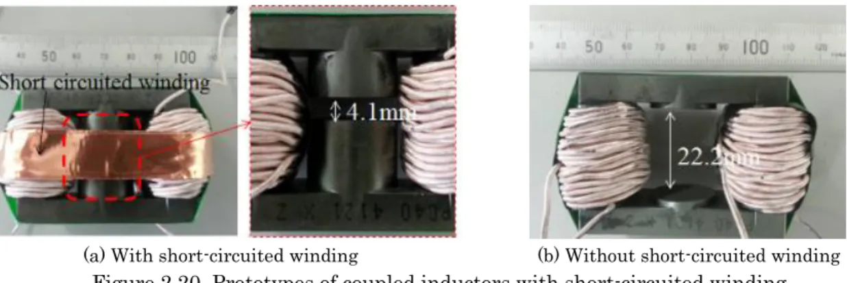
2.8 Short-Circuited Winding Technique ... 27
2.8.1 Short-circuited winding approach ... 28
2.8.2 Experimental results of the SCW ... 29
2.9 Conclusions ... 31
References ... 33
3. Recovery-Less Boost Converter... 35
3.1 Introduction ... 35
3.2 Conventional Tapped-Inductor Converter with Auxiliary Inductor ... 36
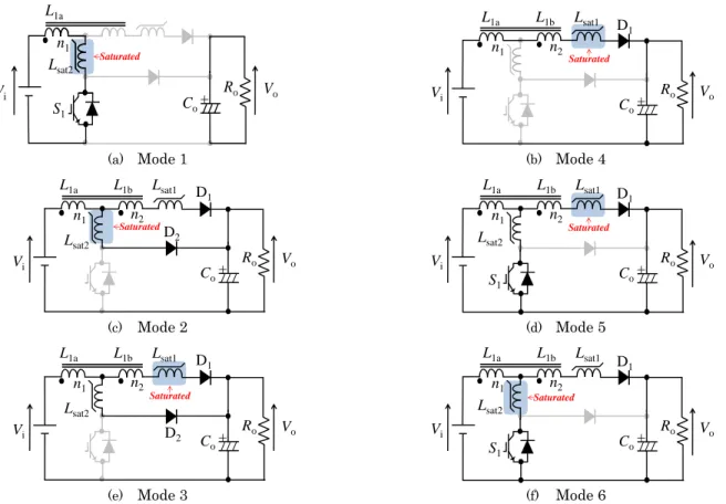
3.3 Single-Phase Recovery-Less Boost Converter ... 38
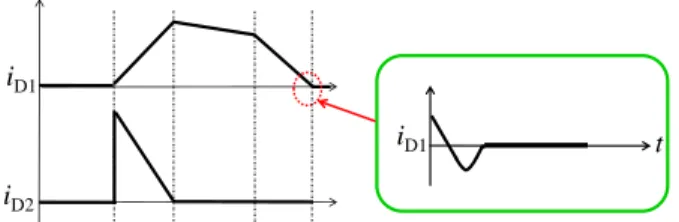
3.3.1 Suppression of the recovery phenomenon ... 41
3.3.2 Design of the saturable inductors ... 42
3.3.3 Experimental validation ... 44
3.4 Two-Phase Interleaved Boost Converter with Saturable Inductors ... 48
3.4.1 Operating Principle ... 49
3.4.2 Suppression of the recovery phenomenon and ZSC behavior ... 54
3.4.3 Experimental validation ... 55
3.5 Conclusions ... 59
References ... 61
4. High Step-Down Converter ... 63
4.1 Introduction ... 63
4.2 High Step-Down Converter ... 64
4.3 Analysis of the Step-Down Conversion Ratio ... 66
4.4 Comparison with Conventional Topologies ... 69
4.5 Experimental Validation ... 70
4.6 Conclusions ... 73
References ... 74
5. High Step-Up Interleaved Boost Converter ... 77
5.1 Introduction ... 77
5.2 High Step-Up Converter ... 78
5.2.1 Steady state analysis ... 80
5.2.2 Central winding operation ... 82
5.2.3 Voltage-gain derivation ... 83
5.2.4 Experimental validation of the HSU comparison ... 85
5.3 Analysis of Coupled Inductor Configuration ... 86
5.3.1 Coupled-inductor configurations ... 87
5.3.2 Magnetic modeling ... 88
5.3.3 Experimental validation ... 92
5.4 Comparison of HSU converters ... 94
5.5 Parasitic Resistance Analysis ... 96
5.5.1 Parasitic resistance effect ... 97
5.6 Parasitic Analysis Comparison ... 103
5.6.1 Interleaved boost converter ...103
5.6.2 Interleaved tapped-inductor converter ...104
5.6.3 Super tapped-inductor converter ...105
5.6.4 Voltage-gain comparison ...107
5.7 Magnetic Flux Modeling ... 109
5.7.1 Validation ...113 5.8 Conclusions ... 115 References ... 117 6. Conclusions ... 119 Publications ... 121 Acknowledgements ... 124
List of Figures
Page.
Figure 1.1. Electric systems in EV applications. ... 2
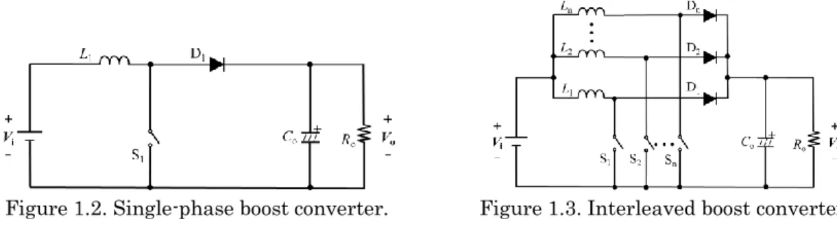
Figure 1.2. Single-phase boost converter. ... 3
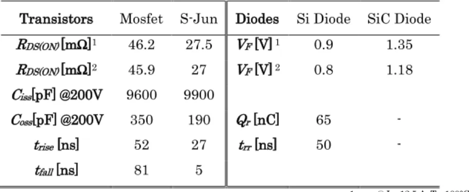
Figure 1.3. Interleaved boost converter. ... 3
Figure 2.1. Interleaved boost converter with integrated magnetic components: LCI, CCI and IWCI ... 10
Figure 2.2. Core geometries. ... 12
Figure 2.3. Winding geometries. ... 13
Figure 2.4. Magnetic circuit models. ... 15
Figure 2.5. Inductor volume vs. inductor losses. ... 17
Figure 2.6. Thermal circuit. ... 18
Figure 2.7. Heat sink geometry. ... 19
Figure 2.8. Total volume comparison when the inductors have 20 turns. ... 21
Figure 2.9. Total volume comparison at the lowest inductor losses. ... 21
Figure 2.10. Core volume vs. inductor losses. ... 22
Figure 2.11. FEM results in Teslas. ... 23
Figure 2.12. Inductor prototypes. ... 24
Figure 2.13. Capacitor comparison. ... 25
Figure 2.14. Prototypes of the four converters. ... 26
Figure 2.15. Experimental waveforms of the LCI prototype. ... 26
Figure 2.16. Efficiency measurement of the LCI converter. ... 27
Figure 2.17. Temperature rise in the power devices of the LCI converter. ... 27
Figure 2.18. LCI converter... 28
Figure 2.19. Coupled inductor surrounded by a short-circuited winding. ... 29
Figure 2.20. Prototypes of coupled inductors with short-circuited winding. ... 30
Figure 2.21. Experimental waveforms... 30
Figure 2.22. Converter efficiency using the short-circuited winding. ... 31
Figure 2.23. Experimental waveforms including induced current. ... 31
Figure 3.1. Tapped-inductor boost converter. ... 35
Figure 3.2. Conventional tapped-inductor converter with auxiliary inductor. ... 37
Figure 3.3. Single-phase recovery-less boost converter. ... 38
Figure 3.4. Voltage and current waveforms during each mode. ... 39
Figure 3.5. Operating modes. ... 39
Figure 3.6. Commutation current in the conventional recovery-less boost converter with auxiliary inductor. ... 41
Figure 3.7. Commutation current in the proposed converter... 42
Figure 3.8. Diode current rate vs. peak of the recovery current. ... 43
Figure 3.9. Experimental setup of the single phase recovery-less converter... 45
Figure 3.11. Inductor size comparison. ... 46
Figure 3.12. Turning ON process of the switch. ... 46
Figure 3.13. Reduction of recovery phenomenon in the main diode. ... 47
Figure 3.14. Efficiency comparison... 47
Figure 3.15. Conventional interleaved ZCS converter. ... 48
Figure 3.16. Proposed interleaved ZCS boost converter. ... 49
Figure 3.17. Operating waveforms. ... 50
Figure 3.18. Operating modes when D<0.5. ... 50
Figure 3.19. Operating modes when D>0.5. ... 53
Figure 3.20. Diodes commutation current in the proposed converter... 54
Figure 3.21. Diodes commutation current in the conventional converter. ... 55
Figure 3.22. Switch commutation process in the proposed converter. ... 55
Figure 3.23. Experimental setup. ... 56
Figure 3.24. Switches voltages vs. input currents in the proposed converter. ... 57
Figure 3.25. Inductor size comparison. ... 57
Figure 3.26. Voltage and current waveforms of the main diode D1. ... 58
Figure 3.27. Reduction of recovery phenomenon in the main diode D1. ... 58
Figure 3.28. Turning ON process of the switch S1... 59
Figure 4.1. Proposed high step-down two-phase interleaved converter. ... 64
Figure 4.2. Coupled-inductor with 3 windings for a HSD converter. ... 64
Figure 4.3. Operating modes of the HSD converter. ... 65
Figure 4.4. Operating waveforms. ... 65
Figure 4.5. Magnetic fluxes in the coupled-inductor with 3 windings... 66
Figure 4.6. Conversion ratio comparison. ... 69
Figure 4.7. Step-down ratio of the proposed converter vs. other topologies. ... 70
Figure 4.8. Prototype of the proposed high step-down converter. ... 72
Figure 4.9. Experimental step-down conversion ratio. ... 72
Figure 5.1. High step-up converter with coupled inductor. ... 79
Figure 5.2. Coupled-inductor with 3 windings for a HSU converter. ... 79
Figure 5.3. Bidirectional high step-up converter. ... 79
Figure 5.4. Operating waveforms. ... 80
Figure 5.5. Operating modes. ... 80
Figure 5.6. Magnetic flux in the coupled-inductor. ... 82
Figure 5.7. Voltage-gain of the proposed converter vs. conventional boost converters. ... 84
Figure 5.8. Experimental Results. ... 86
Figure 5.9. Two cores coupled-inductor. ... 87
Figure 5.10. Magnetic flux in the integrated coupled-inductor. ... 87
Figure 5.11. Magnetic flux in the two cores coupled-inductor... 88
Figure 5.12. General magnetic circuit model. ... 88
Figure 5.13. ICI magnetic circuit model. ... 89
Figure 5.14. TCCI magnetic circuit model. ... 89
Figure 5.15. Equivalent circuit of each independent core in the TCCI configuration. ... 90
Figure 5.16. Experimental setup. ... 92
Figure 5.17. Voltage-gain vs. duty cycle. ... 93
Figure 5.18. Winding current of the ICI prototype. ... 93
Figure 5.19. Input current of the ICI prototype. ... 94
Figure 5.20. Voltage-gain comparison according to the duty cycle. ... 96
Figure 5.22. HSU converter with parasitic winding resistances. ... 97
Figure 5.23. Operating modes of the converter with parasitic resistance. ... 98
Figure 5.24. Non-Ideal conversion ratio vs. Duty cycle. ... 100
Figure 5.25. Conversion ratio tested vs. Duty cycle. ... 102
Figure 5.26. Ideal, theoretical and tested performance with RL/Ro=0.0035. ... 102
Figure 5.27. Efficiency tested vs. duty cycle. ... 103
Figure 5.28. Two-phase interleaved boost converter with parasitic resistances. ... 104
Figure 5.29. Non-ideal voltage-gain of the interleaved boost converter. ... 104
Figure 5.30. Interleaved tapped-inductor converter with parasitic resistances. ... 105
Figure 5.31. Non-ideal voltage-gain of the tapped-inductor converter. ... 105
Figure 5.32. Super tapped-inductor converter with parasitic resistances. ... 106
Figure 5.33. Non-ideal voltage-gain of the super tapped-inductor converter for RL1/Ro =0.1-0.001. ... 106
Figure 5.34. Non-ideal voltage-gain of the super tapped-inductor converter for RL1/Ro=0.001-0.0005. ... 107
Figure 5.35. Voltage-gain comparison of the selected converters. ... 108
Figure 5.36. Non-ideal voltage-gain comparison of the selected converters. ... 109
Figure 5.37. External legs flux waveforms (D<0.5)... 110
Figure 5.38. Flux factor N-D(1+2N). ... 111
Figure 5.39. External legs flux waveform (D>0.5). ... 112
Figure 5.40. Central leg flux waveforms. ... 112
Figure 5.41. Simulated circuit. ... 113
Figure 5.42. Simulation results at D=0.27 (D<0.5). ... 114
Figure 5.43. Simulation results at D=0.8 (D>0.5). ... 114
List of Tables
Page.
Table 2.1.Converter Parameters for Two-Phase Converter Evaluation ... 11
Table 2.2.Power Semiconductors Characteristics ... 18
Table 2.3.Power Semiconductors Losses ... 18
Table 2.4. Heat Sink Parameters and Dimensions ... 20
Table 2.5.Heat Sink Volume ... 21
Table 2.6. Capacitor Comparison ... 25
Table 2.7.Circuit Parameters of the Interleaved Boost Converter ... 29
Table 2.8. Magnetic Parameters ... 29
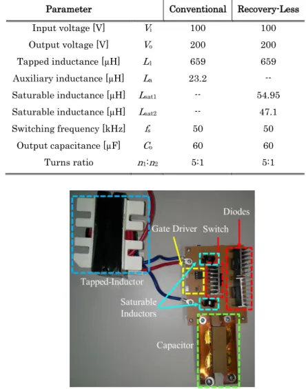
Table 3.1. Design Parameters of the Conventional and the Recovery-Less Circuit ... 45
Table 3.2 Design Parameters of the Conventional and ZCS Interleaved Converter ... 56
Table 4.1 HSD Converters Comparison ... 70
Table 4.2 Experimental Parameters for HSD Evaluation ... 71
Table 4.3 Inductor Parameters for HSD Evaluation ... 71
Table 5.1 Experimental Parameters for the Number of Turns Comparison ... 85
Table 5.2 Inductor Parameters for the Number of Turns Comparison. ... 85
Table 5.3 Experimental Parameters for Inductor Configuration Evaluation. ... 92
Table 5.4 HSU Converters Comparison ... 95
Table 5.5 Experimental Parameters for Parasitic Analysis of the HSU... 101
Table 5.6 HSU Converters Comparison (Including Parasitic Resistances). ... 108
Table 5.7 Winding voltage and AC flux equations when D<0.5 ... 110
1. Introduction
In recent times, there has been a global concern regarding the environmental impacts of the global warming, the resources depletion, and the health problems increase related to the diseases brought by the fossil fuels burning and the greenhouse emissions [1].
In fact, 2016 has been reported as the hottest year ever with a record of 9.4°C of anomaly in certain areas of the planet versus the temperature records of the period between 1951 and 1980 [2]. This is a critical situation due to the harmful impacts that the global warming produces. The main cause of this temperature increase is the greenhouse effect. This phenomenon is produced by the accumulation of greenhouse gasses: CO2, NOx, CO, Sox, among others. Consequently, the energy that comes from the sun everyday cannot be released because of the greenhouse layer. Thereby, earth is continuously adsorbing this solar radiation and becoming heated [3].
These problems are mainly produced by the transport, energy, and heavy industries, just to give an example. These industries constitute an important source of the CO2, NOx, CO, SOx among others polluting gases [4]. In 2014, the United States reported 6.87 Gigatons of CO2 emissions. From this amount, 30% was produced by the energy generation, 26% by the transportation sector and 21% by the industry [5].
In addition, from these emissions produced by the transportation systems, 76% is generated by road transport (automobiles, trucks, etc.), 12% by air traffic, 10% by shipping, and only a 2% by rail traffic [6]. In this context, it is important to highlight the huge impact of the energy generation and transportation systems, especially the road transport, on the global warming and all its effects.
1.1 Power electronics in Renewable Energies and Electric
Vehicle applications
The situation mentioned above calls for the development of renewable energies and electric transportation to contribute with solutions that help tackle these environmental issues [7]-[9]. In this context, power electronics plays a huge role because through it the efficiency of electric systems can be improved, reducing energy consumption. Especially, power converters are key subsystems in applications where power circuits interface renewable energy sources with loads, as well as energy storage units to electric motors in case of electric automotive applications (EVs applications). These applications cover the
concept of vehicles that use an electric motor for the motion of the vehicle, i.e. all the types of Hybrid Electric Vehicles (HEVs), Fuel Cell Electric Vehicles (FCEVs), and pure Electric Vehicles [10]-[16].
These automotive applications present volume and mass problems due to the following reasons: 1) EVs need heavy storage units in order to offer an acceptable autonomy to be competitive with the Internal Combustion Engine (ICE) vehicles. 2) Low efficiency electric systems produce an increase of volume and mass because additional stored energy is required to supply the power losses. And, 3) Bulky and heavy electric systems produce and excess of mass and volume because additional stored energy is needed to supply the energy to move these electric systems. To help tackle these issues, high power density DC-DC converters have attracted considerable attention in the last years [17]-[23].
Consequently, downsizing of the electric powertrains in EV applications becomes essential to increase their performance. Specifically, if the DC-DC converter that interfaces the storage unit with the electric motor is downsized, the energy from the storage devices will be better used because the vehicle systems will be lighter and smaller [24]-[27]. Figure 1.1(a) shows the electric power train of several EV applications where a step-up DC-DC converter is used to boost the voltage of the storage unit in order to achieve the voltage of the motor. Figure 1.1(b) shows the electrical system needed to feed the auxiliary systems, where a step-down DC-DC converter is required.
(a) Electric power train (b) Auxiliary systems
Figure 1.1. Electric systems in EV applications.
1.2 Isolated and Non-Isolated converters
There are two types of DC-DC converters: Isolated and Non-Isolated. The main difference between these two types is the dielectric isolation between the input and the output networks. In other words, isolated converters do not present an electric contact between the input and the output circuits. Isolated converters offer the advantages of 1) in the absence of electric contact, a safety condition is produced for both the input and the output circuit, as well as for the personnel or the circuit user. This condition is presented because three will not be an electric current transmission in case of a circuit failure; 2) Following the previous concept, the isolation between the circuits also prevents the transmission to the output of voltage transients produced in the input side. This transmission absence generated a great blocking capability of noise and interferences: and, 3) Isolated converters can offer different grounding configurations: Negative or positive ground, or even floating ground. Therefore, these converters can be configured to provide negative or positive voltages depending on the load. Isolated converters are widely used in communications where loads are highly sensitive [28]-[30].
Nevertheless, isolated converters present drawbacks of big size. Usually, these converters use bulky transformers and more components that non-isolated converters. Thus, volume, mass, cost, and power losses in some cases of isolated converters are bigger than the case of non-isolated converters.
Non-isolated DC-DC converters offer the advantages of lower cost, and high power density. Consequently, in applications of electric mobility where the DC-DC converters of Figure 1.1 are not continuously connected to the grid, non-isolated converters are suitable candidates to be installed in these applications [31].
1.3 Multi-phase and magnetic integration in Non-Isolated
converters
EV applications have conventionally used non-isolated converter topologies like the well-known single-phase boost converter. Figure 1.2 shows the schematic of a single-phase boost converter [32]-[37]. This topology presents some drawbacks that may decrease the vehicle performance. Among those are recognized: 1) switches and diodes are operated under hard switching which produce EMI/RFI noises and large switching losses; 2) Large conduction losses in the windings and in the power devices are produced by the large peak current generated when the voltage of the storage unit is quite lower than the output voltage. This behavior results from the high duty cycle produced to obtain a high voltage-gain; and 3) large mass and volume of the cooling system due to additional components employed for dissipating power losses. Consequently, novel techniques, that offer reduction of mass and volume as well as efficiency increase, are required for these EV applications.
Figure 1.2. Single-phase boost converter. Figure 1.3. Interleaved boost converter.
Consequently, interleaving phases and magnetic coupling are studied in this document in order to offer solutions to the problems described before. Interleaving-phases is an effective technique because it offers the following advantages: 1) input current is divided into the number of phases. Therefore, a reduction in the power ratings of the components is generated, and this may cause a reduction of the power losses and therefore a heat sink volume reduction; 2) a size miniaturization of the capacitive components results from the high frequency operation produced by the power transmission alternation in each phase; 3) Electromagnetic Interference (EMI) suppression is presented when the number of phases in interleaved converters is increased or when the phase shift is changed.
Figure 1.3 shows the schematic of an interleaved boost converter with n-phases. Nevertheless, interleaving technique presents the disadvantage of increasing the volume and weight of the magnetic components because each phase needs its own inductor [38]-[42].
In this context, magnetic coupling is introduced as an effective technique because: 1) DC fluxes generated by DC currents can be effectively canceled when an inversely coupling is used. In addition, the AC flux may be reduced in certain parts of the core. Therefore, a size reduction of the magnetic components may result from the integration of several windings into only one core. 2) Inductor current ripples in each phase can be reduced due to the mutual effect. As a result, smaller inductances in each phase can be used for realizing the same inductor ripple currents of non-coupled inductors. 3) Transient response speed is improved because the inductor current rate becomes higher than the one of the non-coupled inductor [43]-[49].
1.4 Outline of the thesis
This document presents the volume analysis of outstanding two-phase DC-DC converters. In addition, it proposes four topologies of DC-DC converters using the techniques of interleaving phases and magnetic coupling. Chapter 2 presents a review of the two-phase interleaved boost converter with coupled-inductors. Volume and efficiency trends are studied and evaluated. Chapter 3 proposes a single-phase and a two-phase DC-DC converter for reducing the recovery losses on the power diodes. These converters offer the novelty of the inclusion of saturable inductors with the purpose of reducing the slope of the diode current and thereby the reverse recovery reduction. Chapters 4 and 5 present the application of magnetic integration and interleaving phases for obtaining high voltage-gains. As it was explained above, conventional converters often present some problems when a high voltage-gain is required to produce it, a large duty cycle and large currents are needed. These conditions increase the conduction losses especially caused by the parasitic components, and in most cases a high voltage-gain is not reached because of these losses. Consequently. Chapter 4 derives a method for achieving a high step-down ratio in a converter aimed to be applied for low voltage systems in EV applications (Figure 1.1 (b)) or in renewable energy applications. Chapter 5 proposes a high voltage-gain converter using the technique of chapter 4. In chapters 4 and 5, the study of the high voltage-gain converters is conducted through the steady state analysis, comparison with outstanding converters reported in the literature, and the analysis of the effect of parasitic components on the voltage gain. Finally, conclusions are given to this document as well as the list of publications resulting of this research.
References
[1] IARC – International Agency for Research on Cancer, “Diesel Engine Exhaust Carcinogenic,” World Health Organization. pp. 1-4. 2012.
[2] GISS Surface Temperature Analysis (GISTEMP) Retrieved from http://data.giss.nasa.gov/gistemp/. [3] C. Gibbs, and M. Cassidy, “2 Crimes in the carbon market,” Handbook of Transnational Environmental
Crime, 235. 2016.
[4] UNFCC –United Nations Framework Convention on Climate Change. “National greenhouse gas inventories,” Unfccc Resource Guide. p. 31. 2010.
[5] EPA – US Environmental Protection Agency, “U.S. Greenhouse Gas Inventory Report: 1990-2014,” Retrieved from https://www3.epa.gov/climatechange/ghgemissions/usinventoryreport.html
[6] IEA-International Energy Agency, “Energy and Climate Change,” World Energy Outlook Special Report, 2015.
[7] J. Dixon, M. Ortuzar, and E. Wiechmann, “Regenerative Braking for an Electric Vehicle Using Ultracapacitors and a Buck-Boost Converter” Catholic University of Chile. pp. 1-4. 2008.
[8] C. Bonfiglio and W. Roessler, “A Cost Optimized Battery Management System with Active Cell Balancing for Lithium Ion Battery Stacks”, Vehicle Power and Propulsion Conference, VPPC ’09, pp. 304 - 309. 2009. [9] C. Shumei, L. Chen and S Liwei, “Study on efficiency calculation model of induction motors for electric
vehicle”, IEEE Vehicle Power and Propulsion Conference, VPPC ’08, pp. 1-5. 2008.
[10] I. Aharon and A. Kuperman, “Topological Overview of Powertrains for Battery-Powered Vehicles with Range Extenders” IEEE transactions on power electronics, Vol 26, no. 3, pp. 867 -870. 2011.
[11] A. Burke, “Batteries and Ultracapacitors for Electric, Hybrid, and Fuel Cell Vehicles”, Proceedings of the IEEE, Vol 95, pp. 808 - 811. 2007.
[12] A. Burke, “Ultracapacitors: why, how, and where is the technology”, Journal of power sources, vol. 91, pp. 37-50, 2000.
[13] J. Dixon, I. Nakashima, E. Arcos and M. Artuzar, “Electric vehicle using a combination of ultracapacitors and zebra battery”, IEEE transactions on industrial electronics, Vol 57, pp. 943 - 947. 2010.
[14] T. Gillespie, “Fundamentals of vehicle dynamics”, 1st Ed., SAE International, 1992.
[15] P. Bossche, F. Vergels, J. Mierlo, J, Matheys and W. Autenboer, “SUBAT: An assessment of sustainable battery technology”, Journal of Power Sources (2005), Vol 162. Pp. 913-919. 2005.
[16] International Energy Agency – IEA, “Technology Roadmap Electric and plug-in hybrid electric vehicles (EV/PHEV)”, pp. 10 - 14. 2011.
[17] H. Zhai, “Comparison of Flexible Fuel Vehicle and Life-Cycle Fuel Consumption and Emissions of Selected Pollutants and Greenhouse Gases for Ethanol 85 Versus Gasoline,” Journal of the Air & Waste Management Association, Vol. 59 no. 8, pp. 912-24. 2009.
[18] R. Kemp et al., Electric Vehicles: Charged with Potential. London, U.K.: Royal Academy of Engineering, 2010.
[19] S. Peeta and A. K. Ziliaskopoulos, “Foundations of dynamic traffic assignment: The past, the present and the future,” Netw. Spatial Econ., vol. 1, no. 3/4, pp. 233–265, Sep. 2001.
[20] W. Martinez, C. Cortes and L. Munoz, “Sizing of Ultracapacitors and Batteries for a High Performance Electric Vehicle,” IEEE International Electric Vehicle Conference (IEVC), pp. 535-541. 2012.
[21] IEA, Energy Technology Perspectives, scenarios & strategies to 2050 by International Energy Agency, 2010.
[22] J. Bishop, et al., “Investigating the technical, economic and environmental performance of electric vehicles in the real-world: A case study using electric scooters,” Journal of Power Sources, Vol. 196, pp. 10094–10104. 2011.
[23] P. Baptista, M. Tomas, C. Silva, “Plug-in hybrid fuel cell vehicles market penetration scenarios,” International Journal of Hydrogen Energy, Vol. 35 no. 18, pp. 10024- 10030. 2010.
[24] Y. Cheng, R. Trigui, C. Espanet, A. Bouscayrol, and S. Cui, “Specifications and Design of a PM Electric Variable Transmission for Toyota Prius II,” IEEE Trans. on Vehicular Technology, vol. 60, no.9, pp.4106-4114, Nov. 2011.
[25] M. Pavlovsky, Y. Tsuruta, A. Kawamura, “Recent improvements of efficiency and power density of DC-DC converters for automotive applications”, The 2010 International Power Electronics Conference (IPEC), pp.1866-1873, 2010.
[26] C. Chan, A. Bouscayrol, K. Chen, “Electric, Hybrid, and Fuel-Cell Vehicles: Architectures and Modeling”, IEEE Transactions on Veh. Technol., vol. 59, no. 2, pp. 589-598, 2010.
[27] M. Yilmaz and P. Krein, “Review of Battery Charger Topologies, Charging Power Levels, and Infrastructure for Plug-In Electric and Hybrid Vehicles,” IEEE Trans. on Power Electronics, vol. 28, no. 5, pp. 2151-2169, May. 2013.
[28] H. Mao, L. Yao, J. Liu, and I. Batarseh, “Comparison study of inductors current sharing in non-isolated and isolated DC-DC converters with interleaved structures,”. 31st Annual Conference of IEEE Industrial Electronics Society, IECON pp. 1-7, 2005.
[29] M. Prudente, L. Pfitscher, G. Emmendoerfer, E. Romaneli, and R. Gules, R. “Voltage multiplier cells applied to non-isolated DC–DC converters,” IEEE Transactions on Power Electronics, 23(2), 871-887. 2008.
[30] Y. Du, X. Zhou, S. Bai, S. Lukic, and A. Huang, “Review of non-isolated bi-directional DC-DC converters for plug-in hybrid electric vehicle charge station application at municipal parking decks,” Applied Power Electronics Conference and Exposition (APEC), pp. 1145-1151. 2008.
[31] W. Li, X. Lv, Y. Deng, J. Liu, and X. He, “A review of non-isolated high step-up DC/DC converters in renewable energy applications,” Applied Power Electronics Conference and Exposition, APEC, pp. 364-369, 2009.
[32] F. Guedon, S. Singh, R. McMahon and F. Udrea, “Boost Converter with SiC JFETs: Comparison with CoolMOS and Tests at Elevated Case Temperature,” IEEE Transactions on Power Electronics, vol.28, no.4, pp.1938-1945, 2013.
[33] Toyota Motor Corporation, “Toyota Prius V Hybrid Vehicle Dismantling Manual”, pp. 1-30, 2011. [34] W. Li and X. He, “ZVT interleaved boost converters for high-efficiency, high step-up DC-DC conversion,”
IET Trans. Power Electron., vol. 1, no. 2, pp. 284–290, 2007.
[35] R. Wai, C. Lin, R. Duan and Y. Chang, “High-efficiency DC–DC converter with high voltage gain and reduced switch stress”, IEEE Trans. Ind. Electron., vol. 54, no. 1, pp. 354–364, 2007.
[36] R. Erickson and D. Maksimovic: “Fundamentals of Power Electronics”, 2nd ed. Norwell, MA: Kluwer, 2001.
[37] Y. Zhao; W. Li and X. He: “Single-Phase Improved Active Clamp Coupled-Inductor-Based Converter with Extended Voltage Doubler Cell” IEEE Transactions on Power Electronics, vol.27, no.6, pp.2869,2878, 2012.
[38] K. Katsura and M. Yamamoto, “Optimal stability control method for transformer-linked three-phase boost chopper circuit,” IEEE Energy Conversion Congress and Exposition (ECCE), pp. 1082–1087. 2012. [39] L. Tang and G. Su, “An Interleaved Reduced-Component-Count Multivoltage Bus DC/DC Converter for Fuel Cell Powered Electric Vehicle Applications”, IEEE Trans. on Industry Applications, vol. 44, no. 5, pp. 1638-1644, Sep. 2008.
[40] F. Yang, X. Ruan, Y. Yang, Z. Ye, “Interleaved Critical Current Mode Boost PFC Converter with Coupled Inductor,” IEEE Trans. Power Electron., vol.26, no. 9, pp. 2404-2413, 2011.
[41] J. Gu, J. Lai, N. Kees, and C. Zheng, “Hybrid-Switching Full-Bridge DC–DC Converter with Minimal Voltage Stress of Bridge Rectifier, Reduced Circulating Losses, and Filter Requirement for Electric Vehicle Battery Chargers,” IEEE Trans. on Power Electronics, vol. 28, no.3, pp.1132-1144, Mar. 2013. [42] U. Sebastian, P, Johannes, “Current-balancing Controller Requirements of Automotive Multi-Phase
Converters with Coupled Inductors”, Proc. IEEE Energy Conver. Cong. Expo. (ECCE), pp. 372-379, 2012. [43] S. Kimura, J. Imaoka and M. Yamamoto, “Potential power analysis and evaluation for interleaved boost converter with close-coupled inductor”, IEEE 10th International Conference on Power Electronics and Drive Systems (PEDS), pp.26-31, 2013.
[44] Y. Suh, T. Kang, H. Park, B. Kang and S. Kim, “Bi-directional Power Flow Rapid Charging System Using Coupled Inductor for Electric Vehicle”, IEEE Energy Conversion Congress and Expo (ECCE2012), pp. 3387-3394, 2010.
[45] M. Hirakawa, Y. Watanabe, M. Nagano, K. Andoh, S. Nakatomi, S. Hashino and T. Shimizu, “High Power DC/DC Converter using Extreme Close-Coupled Inductors aimed for Electric Vehicles”, Proc. the 2010 international Power Electron. Conf. (ECCE ASIA 2010), pp.2941-2948 ,2010
[46] K. J. Hartnett, J. G. Hayes, M. G. Egan, M. S. Rylko, “CCTT-Core Split-Winding Integrated Magnetic for High-power DC-DC Converters”, IEEE Trans. Power Electron, Vol.28. pp. 4970-4984, 2013.
[47] J. Imaoka, Y. Ishikura, T. Kawashima, M. Yamamoto, “Optimal Design Method for Interleaved Single-phase PFC Converter with Coupled Inductor”, IEEE Energy Conversion Congress and Expo (ECCE2011), pp. 1807-1812, 2011.
[48] J. C. Schroeder and F. W. Fuchs, “Detailed Characterization of Coupled Inductors in Interleaved Converters Regarding the Demand for Additional Filtering”, Proc. IEEE Energy Conver. Cong. and Expo. (ECCE), pp.759-766, 2012.
[49] M. Pavlovsky, G. Guidi and A. Kawamura, “Assessment of Coupled and Independent Phase Designs of Interleaved Multiphase Buck/Boost DC–DC Converter for EV Power Train,” IEEE Trans. on Power Electronics, vol. 29, no.6, pp. 2693-2704, Jun. 2014.
2. Two-Phase Interleaved Boost
Converter
2.1 Introduction
Many converter topologies reported as effective for electric mobility applications have been proposed [1],[2],[4], [7]-[17]. Each topology offers different advantages for the vehicle performance. However, in order to evaluate the power density characteristics of these topologies, a volume comparison is required. Thereby, based on this characterization a design criterion to downsize the electric power train of the vehicle is proposed.
This chapter presents the electric and magnetic analysis of inductor arrangements using the magnetic coupling technique to the two-phase interleaved boost converter. These topologies appear as promising candidates to be applied in EV applications. Specifically, the studied arrangements are the topologies with Loosely Coupled-Inductor (LCI) and Closed Coupled-Inductor (CCI). In addition, in this chapter the recently proposed arrangement of the Integrated Winding Coupled-Inductor (IWCI) is also reviewed. Figure 2.1 shows the schematics of these three magnetic components.
It is important to mention that CCI is divided into a single winding inductor and a transformer achieving higher filtering because of the sum of two magnetic components. In addition, in the CCI converter, different core materials can be selected for the inductor and the transformer, e.g. the single inductor can be made of high flux density materials (Amorphous, Nanocrystaline, Powder, etc.) while the transformer can use Ferrites [16]. However, the CCI evaluation and comparison is not conducted because the interleaved circuit with LCI integrates the concept of inductor and transformer of the CCI converter into only one core resulting in a direct reduction of the number of magnetic cores. Therefore, the LCI is evaluated instead of the CCI.
Additionally, the conventional single-phase boost converter with only one magnetic component, and the two-phase interleaved boost converter with non-coupled inductors (two magnetic components) are evaluated with the purpose of showing the outstanding advantages of the interleaving phases and the magnetic coupling techniques.
Figure 2.1. Interleaved boost converter with integrated magnetic components: LCI, CCI and IWCI
In Figure 2.1, L corresponds to the self-inductances; M are the mutual inductances between the windings; and N are the number of turns of each winding. In addition, in order to evaluate the magnetic coupling technique, the two-phase interleaved boost converter with non-coupled inductors is considered as well.
These topologies were selected because the interleaving-phases technique is expected to downsize the output capacitor, as a higher frequency is achieved by power transmission alternation in each phase [20]. In addition, the magnetic coupling technique is effective because the inductor current ripple presents a higher frequency behavior, and DC fluxes can be cancelled due to the mutual induction effect [15].
The analysis is conducted in several steps: 1) Geometry sizing of each magnetic component is calculated considering the inductor model; 2) Power losses of each magnetic component are calculated with the purpose of obtaining the efficiency of each inductor; 3) Semiconductor power loss calculation is carried out for sizing the required cooling device needed to dissipate these losses; 4) Finally, the total volume of each converter is evaluated and compared. As an evaluation example, the volume and the power loss analyses are conducted on four converters having the parameters shown in Table 2.1.
The parameters of Table I were selected as a model of the DC-DC converter of the Toyota Prius III. This scale model is set as 1/60 of the power of the Prius’ converter and it was chosen due to the available equipment for tests and safety conditions. This case study will suggest the qualitative advantages and disadvantages of the four topologies by the volume evaluation of their entire structure.
Table 2.1.Converter Parameters for Two-Phase Converter Evaluation
Parameters Value Input Voltage [V] 80 Output Voltage [V] 200 Power [kW] 1 Switching Frequency [kHz] 50 Duty Cycle 0.6
Input Ripple Current [%] 20 Output Ripple Voltage [%] 0.1
2.2 Inductor Sizing
In order to conduct the volume evaluation of the selected topologies, inductor volume sizing and loss calculations are required. Thus, the definition of the core and winding geometries is presented as the base of the volume and power loss analysis. In this section, the size of each inductor is analyzed considering a Continuous Current Mode (CCM) condition. This is because magnetic components are usually designed at maximum ratings, and Discontinuous Current Mode (DCM) is not effective in high power applications because conduction losses tend to increase.
2.2.1
Core size
Volume analysis of the inductors of each topology is carried out based on the core modeling with the geometries presented in Figure 2.2. Usually, non-coupled inductors can use two-leg cores (conventionally CC, CI or U cores) or in some cases three-leg cores. Figure 2.2(a) shows the dimensions of the geometry for non-coupled inductors, and, Figure 2.2(b) shows the geometry dimensions for the three-leg cores (usually EE, EI, EC or EER cores) used by the LCI and IWCI converter. These types of geometries employ a central leg because of the increasing of the leakage inductance.
With the purpose of simplifying the calculation of the dimensions and thereby the volume of the core, most of the dimensions are set according to the sectional area of the core Ae. Moreover, the sectional areas and the window areas are assumed as squares for
convenience in the calculation.
The selected core material for this evaluation example is a TDK ferrite of reference PC40, with a saturation flux density of 380mT at 100°C, a remanent flux density of 125mT,
and a relative permeability of 2300. Consequently, for these analyses, we set a maximum flux density of 250mT.
(a) Core geometry for Single-Phase and
Interleaved converters (b) Core geometry for LCI and IWCI converters Figure 2.2. Core geometries.
2.2.2
Core losses
Core losses are mainly dependent on the eddy currents and the hysteresis process, and can be calculated by the well-known Steinmetz Equation (SE) [20]-[23]. However, this calculation method is limited because it is valid only under a sinusoidal excitation condition. For this problem, the improved Generalized Steinmetz Equation (iGSE) was proposed [21]. In this context, using the SE parameters of the PC40 material, the core losses can be calculated as follows:
ΔB dt dt dB k T P T
sw 0 i sw cv 1 (2.1)
2 0 1 i2
cos
2
d
k
k
(2.2)where dB/dt is the slope of the flux density; ∆B is the peak-to-peak flux density; Tsw is the
switching period; and Vc is the volume of the core. k, α, β are the Steinmetz parameters
obtained from the datasheets of the PC40 core material. In the example case, k =4.5×10⁻¹⁴, α=1.55, and β=2.5. ki can be calculated by applying these parameters to equation (2.2),
and core losses per volume is obtained from (2.1) [20],[24].
2.2.3
Winding size
Winding volume is calculated to complete the total inductor volume. This analysis is conducted on the base of the winding geometry illustrated in Figure 2.3(a). As well as the core geometry description, winding geometry was set as squared for convenience in the
e A Ae Aw w A w A Window area Sectional area e A w A e A e A e A Aw e A e A e A Ae Aw w A w A Sectional area of the external leg
Window area w A w A e A c W e A e A e A
calculation. In addition, the winding volume is calculated in accordance with the sectional area of the surrounded core, see Figure 2.2 and Figure 2.3.
(a) Winding geometry (b) Winding resistances geometry
Figure 2.3. Winding geometries.
2.2.4
Winding losses
Finally, the calculation of the winding losses is needed to complete the inductor efficiency analysis. These losses are generated by the DC resistance of the total winding and the AC resistance affected by the skin-effect. Figure 2.3(b) shows the geometry of each resistance. Winding losses are derived as follows:
2 2 Lrms AC L DC winding R I R I P (2.3)
where RDC and RACare the DC and AC (at high frequency) resistance respectively, IL is the
DC component of the inductor current, and ΔILrms is the effective value of the inductor
current ripple. In this context, DC resistance is dependent on the length of the winding, the sectional area of the wire and the wire material. In addition, AC resistance, where the skin effect is considered, can be calculated as:
d
l
d
d
l
R
AC 2 22
2
(2.4) sw f 0
(2.5)where ρ is the resistivity of the winding materials, d is the diameter of the wire, l is the winding length, δ is the skin depth, and μ0 is the permeability of the free space.
2.3 Inductor Modeling
After the definition of each geometry that affects the power density and the efficiency of the inductor in the selected topologies, the inductor modeling is conducted. Therefore, regarding the volume comparison, regarding the volume comparison, the behavior of the
2 winding A 2 winding A 2 winding A 2 winding A e
A
e A e A Aw N winding A N winding A winding A winding A winding A DC resistance RDC AC resistance RACmagnetic flux that flows in each magnetic component of the four converters is analyzed. The maximum flux intensity is defined as:
2 max AC DC
(2.6)where ΦDC and ΦAC are the average and the peak-to-peak magnetic fluxes in the core. The
derivation of the maximum flux in each of the four topologies is presented in [11]-[19]. The required sectional area can be calculated with the derived magnetic flux of each topology and the maximum magnetic flux density of the selected material (Ae=Φmax/Bmax).
In the case of the four topologies evaluated in this study, their maximum magnetic flux density has been previously derived and presented in [12]-[19].
2.3.1
Single phase converter
The single-phase boost converter has only one inductor with one winding of N turns. Based on the overall modeling presented in [24], it is possible to derive the sectional area calculation as follows:
sw L L L ax eNf
I
D
V
I
I
B
A
in m)
2
(
1
(2.7)where ΔIL is the ripple current through the inductor, Vin is the input voltage, and D is the
duty cycle.
2.3.2
Interleaved converter with non-coupled inductors
Figure 2.1 shows the two-phase interleaved boost converter with non-coupled inductors. Each inductor has one winding of N turns. Consequently, as it is reported in many studies [12]-[13], the operating principle of this topology is the same as the conventional single-phase boost converter with the exception of the single-phase-shift in the switching process of the switches. Therefore, the sectional area calculation according to the magnetic flux is modeled as follows: sw L in L ph e Nf ΔI D )V ΔI I ( B A 2 2 1 max (2.8)
2.3.3
LCI converter
The modeling of coupled inductors in interleaved boost converters is more complicated than the one of conventional topologies. As Figure 2.1 and Figure 2.2 depict, the loosely-coupled inductor is composed of one core of three legs and two windings, each one of N
turns [14]-[15]. In this context, the sectional area of the external legs of the core as a function of the duty cycle can be calculated from the maximum flux density reported in [14]-[15] as follows:
sw in mo ph e Nf D V R α NI B A 2 1 2 1 1 max (2.9)where Rmo is the magnetic reluctance of the external legs, and α is defined as the ratio of Rmc/Rmo, where Rmc is the reluctance of the central leg. Figure 2.4(a) shows the magnetic
model of the LCI magnetic component.
(a) LCI (b) IWCI
Figure 2.4. Magnetic circuit models.
Considering the behavior of the magnetic flux in the central leg, and based on the maximum flux density derived in [14]-[15], (2.10) shows the calculation of the sectional area when the duty cycle is lower than 0.5. In the same way, (2.11) shows the calculation for the case of duty cycles higher than 0.5.
D D Nf D V R α NI B A sw in mo ph c 1 2 1 2 1 2 1 2 1 max (2.10)
2 1 2 1 2 1 2 1 max D Nf V R α NI B A sw in mo ph c (2.11)2.3.4
IWCI converter
Finally, the integrated winding coupled inductor is composed of one magnetic core with three different windings installed in each leg. Figure 2.4(b) shows the magnetic model of the IWCI component. The numbers of turns are N1 for the central winding and N2 for the
N N Rme Rmc Rme N2 N1 N2 Rme Rme Rmc NiL Rme NiL Rmc Rme N2iL2 Rme N2iL2 Rmc Rme N1iL1
external windings (see Figure 2.1 and Figure 2.2). Consequently, and based on the overall modeling of this magnetic component and the maximum magnetic flux density derivation presented in [17]-[19], (2.12) shows the sectional area of the external legs for the cases of duty cycles lower than 0.5, and (2.13) shows the sectional area calculation for the external legs when the duty cycle is higher than 0.5. In this converter, the operating states are different for duty cycles lower or higher that 0.5, and thereby the sectional area calculation is different for both cases.
D β f N β D V R α I N β B A sw in mo ph e 1 1 2 1 2 1 2 1 2 1 1 2 2 max (2.12)
D β f N β D V R α I .N β B A sw in mo ph e 1 2 1 2 1 2 1 2 1 1 2 2 max (2.13)where β is defined as the ratio of N1/N2 and, for this particular volume study, it is set as β=1. This β is chosen due to the convenience of having the same number of turns because the height of the central and external legs is the same in regular EE cores. Furthermore, (2.14) shows the calculation of the sectional area of the central leg when the duty cycle is lower than 0.5; and, (2.15) shows the case for a duty cycle higher than 0.5.
D D f N β D V R α I N β B A sw in mo ph c 1 2 1 2 1 2 1 2 1 2 1 2 1 2 2 max (2.14)
2 1 2 1 2 1 2 1 2 1 2 1 2 2 max D f N β V R α I N β B A sw in mo ph c (2.15)2.3.5
Volume and losses comparison
A comparison among the selected topologies was performed taking into account the geometric models of cores and windings, their loss models, and the magnetic flux modeling of each topology. This was possible by solving (2.7)-(2.15) with the evaluation of different number of turns, and the calculation of each variable with the parameters defined in Table 2.1.
Figure 2.5 shows the comparison between the volume of each inductor (or pair of inductors in the case of the interleaved converter) and their power losses. This comparison was made considering a varying number of turns in each inductor, because the number of turns influences the core size and the inductor losses (both core and copper losses). Thus, each of the dots on each line corresponds to a value of the number of turns. In addition, the increment of the number of turns produces a reduction in the total inductor volume in each converter. This behavior is generated by the winding-core dependency, where the
lower the number of turns, the larger the core size in order to accomplish the filtering requirements.
Figure 2.5. Inductor volume vs. inductor losses.
Figure 2.5 also shows that LCI and IWCI topologies offer low inductor volume. Moreover, the IWCI can be miniaturized compared with the LCI, but this miniaturization can lead to the increase in the inductor losses, this is because of the trade-off between the core size and the inductor losses. Additionally, it is possible to see the effectiveness of the magnetic coupling technique compared with the non-coupled inductors. Finally, the performance of the LCI converter is remarkable because it presents the lowest power losses with small volume for this case study. Therefore, the magnetic coupling technique is validated as an effective technique for downsizing and, in some cases, for increasing the efficiency of magnetic components.
2.4 Cooling Devices Volume
In order to calculate the volume of the cooling devices, the semiconductor losses and the heat sink modeling are required.
2.4.1
Semiconductor losses
Power losses in semiconductor devices can be classified into: switching and conduction losses that are dependent on the Equivalent Series Resistance (ESR), voltage drops, parasitic capacitances, and parasitic inductances, among others. [25]-[28].
In fact, transistor losses are produced by the static drain-source on-state resistance RDS(ON), the transistor input capacitance, the output capacitance, and the switching transition process. Diode losses are produced by the diode voltage drop, the diode resistance, and the reverse recovery when the converter operates in continuous conduction mode. The overall power loss model is explained in detail in [24].
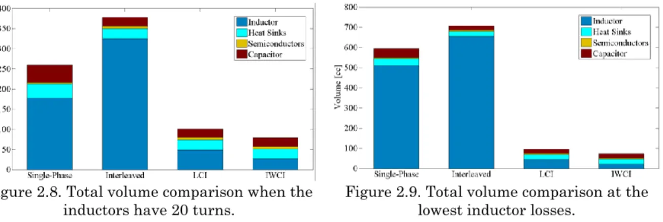
Conventional Silicon and next-generation devices (Super Junction and SiC Devices) were chosen for evaluating their losses and thereby the volume of the required cooling devices. Table 2.2 shows the parameters of the selected semiconductors, taking into
account the voltage and current stresses of each topology. All the selected devices have a TO-247 package and a voltage rating of 650V for the Super-Junction devices and 600V for the other devices.
TABLE 2.2.Power Semiconductors Characteristics Transistors Mosfet S-Jun Diodes Si Diode SiC Diode RDS(ON) [mΩ]1 46.2 27.5 VF [V] 1 0.9 1.35 RDS(ON) [mΩ]2 45.9 27 VF [V] 2 0.8 1.18 Ciss[pF] @200V 9600 9900 Coss[pF] @200V 350 190 Qr[nC] 65 - trise[ns] 52 27 trr[ns] 50 - tfall[ns] 81 5 1 @ ID=12.5 A, TJ=100°C 2 @ ID=6.25 A, TJ=100°C
Based on the power loss model of [24], the parameters of Table 2.1 and the power semiconductors of Table 2.2, the individual power losses of the transistors and diodes of each converter are displayed in Table 2.3.
TABLE 2.3.Power Semiconductors Losses
Single-Phase Interleaved LCI IWCI
Transistor Losses [W]
Si S-Jun Si S-Jun Si S-Jun Si S-Jun
13.11 4.85 5.7 1.91 6.04 2.11 6.04 2.11 Diode Losses [W]
Si SiC Si SiC Si SiC Si SiC
13.28 7.75 5.78 3.2 5.78 3.2 5.78 3.2
2.4.2
Heat sink modeling
The first step to model the semiconductor cooling device (heat sinks are conventionally used for low power dissipation) is to calculate the required thermal resistance from the cooling device to the air [29]. This resistance can be calculated from the thermal circuit presented in Figure 2.6.
Figure 2.6. Thermal circuit.
The junction temperature TJ(defined by the manufacturer) can be calculated using
Loss HA CH JC AMB J T R R R P T ( ) (2.16)
where TAMB is the ambient temperature (usually 50°C for the ambient within the converter
[30]), RΦJC is the thermal resistance from the junction to the semiconductor’s case, RΦCHis
the thermal resistance from the case to the heat sink (usually neglected due to its very small value), RΦHA is the thermal resistance from the heat sink to the air, and PLoss is the
dissipated power in each power device. Thus, using (2.16), it is possible to calculate the required heat sink thermal resistance.
All the selected power devices have a maximum junction temperature of 175°C; however, the heat sink volume calculation is conducted assuming a maximum junction temperature of 100°C with the purpose of protecting the power devices and preventing high ambient temperature rises.
Once the thermal resistance of the heat sink from the base plate surface to the ambient is calculated, the next step is to model the size of the heat sink. Figure 2.7 shows the definitions of the heat sink geometry, and based on [31]-[33], it is possible to derive the thermal resistance of the heat sink in relation to its geometry as follows:
V
c
R
R
R
n
R
air P air A th FIN th d th HA , , , ,5
.
0
2
1
1
(2.17)Figure 2.7. Heat sink geometry.
where n is the number of the channels, ρairis the air density, cp,airis the specific thermal
capacitance of air, V is the air volume flow, and Rth,d is the thermal resistance of the heat
sink base of height d. Rth,d is calculated as follows:
HS HS d th
A
d
n
R
.
,
(2.18)where AHS is the size of the heat sink plate, and λHS is the thermal conductivity of the heat
sink material (generally, heat sinks are manufactured with aluminum alloys). Additionally, Rth,FIN is defined as the thermal resistance of the fins and is expressed as:
b H L c d t s L W HS A n: number of channels n b /
HS FIN th
tL
c
R
, (2.19)where c, t and L are the dimensions of the defined heat sink geometry. Finally, Rth,A is the
thermal resistance between the fin surface and the air channel:
hLc RthA
1
, (2.20)
where h is the convective heat transfer coefficient. The required heat sink dimensions, and thereby its volume, can be calculated by solving (2.17) according to (2.18)-(2.20). This calculation is made using the heat sink parameters shown in Table 2.4. Note that (2.17) presents several variables: s, L, t, d, c, and n. Based on several heat sinks, suitable for the TO-247 package and available in the market, the dimensions s, L, t, d, and c were selected as it is shown in Table 2.4. Using the calculated thermal resistance for the heat sinks, it is possible to derive the number of channels n that the heat sink needs, and therefore its volume is estimated.
TABLE 2.4.Heat Sink Parameters and Dimensions Parameters Value Dimensions Value
h [W/(m2°C)] 25 s [mm] 4 λHS [W/(m°C)] 237 L [mm] 25 V [m3/s] 0.006 t [mm] 1 ρAIR [kg/m3] 0.99 d [mm] 2 cp,AIR [J/(kg°C)] 1010 c [mm] 10
2.5 Volume Comparison
2.5.1
Power devices
When next-generation devices are used instead of conventional Silicon semiconductors, a reduction in power losses and heat sinks volume is produced. Table V shows the volume of the heat sinks set (pair or single) needed to dissipate the losses of each individual semiconductor. This heat sinks set corresponds to one device in the case of the single phase, and two devices in the case of the other three topologies. As a result, the use of next-generation power devices can reduce the power losses and thereby the heat sink volume up to 60% in comparison with the conventional Silicon semiconductors for the case of the defined 1kW prototype.
In addition, in order to have a better understanding of the calculated volume, Table 2.5 reports also the Cooling System Performance Index (CSPI), defined as the power density capability of the cooling system, described in detail in [31].
Table 2.5.Heat Sink Volume
Single-Phase Interleaved LCI IWCI
Transistor Heat Sink Volume [cc]
Si S-Jun Si* S-Jun* Si* S-Jun* Si* S-Jun*
7.18 2.79 6.46 2.54 6.81 2.75 6.81 2.75
CSPI [°C /(W.Liter)]
18.74 17.59 17.86 15.09 17.9 15.44 17.9 15.44 Diode Heat Sink Volume [cc]
Si SiC Si* SiC* Si* SiC* Si* SiC*
6.36 3.7 5.52 3.27 5.52 3.27 5.52 3.27
CSPI [°C /(W.Liter)]
18.66 18.03 17.56 16.13 17.56 16.13 17.56 16.13
*Heat Sink Values of Interleaved, LCI and IWCI correspond to a pair of devices
2.5.2
Total volume
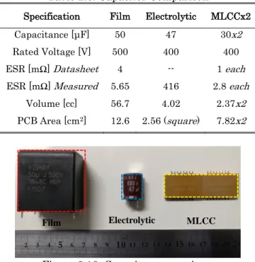
Based on the inductor and the cooling modeling described above, the total volume of the selected topologies under the defined parameters was calculated. Two comparisons were made. The first one compares the volume of the total converter when each magnetic component of the four converters has windings with N=20 turns. This comparison is shown in Figure 2.8. The second comparison shows the converters when the inductors have their lowest power losses (Figure 2.9). These comparisons were calculated using the values of the Super-Junction Mosfet and the SiC Diode, as well as their corresponding heat sinks. For the comparison of Figure 2.8 and Figure 2.9, conventional electrolytic capacitors were used.
Figure 2.8. Total volume comparison when the
inductors have 20 turns. Figure 2.9. Total volume comparison at the lowest inductor losses.
Figure 2.5, Figure 2.8, and Figure 2.9 show the opposition between efficiency and power density, i.e., first, the topology that offers the lowest power losses is the LCI converter, and
second, this topology has a bigger volume in certain numbers of turns in comparison with the other three topologies. On the contrary, the IWCI converter exhibits the smallest volume, but for this case study, it presents the highest power losses.
2.6 Inductor Size Evaluation
In the previous sections, ideal cores with defined geometries (Figure 2.2) have been modeled. These geometries were defined using squares for calculation convenience. However, in practice, it is difficult to find the exact core that fills the design parameters. In this context, there are two possibilities: 1) To use a customized core that fulfills all the design requirements, resulting in an overcost due to the personalized core, or 2) To use a core available in the market that can fulfill the requirements. Consequently, in order to validate the modeling presented so far and compare the changes of efficiency and volume in the defined geometries with cores available in the market, four different cores were selected to be compared with the results exhibited in Figure 2.5. These cores were selected because their volume and effective sectional area fit into the calculated values of Figure 2.5, they are fabricated with the selected core material (TDK ferrite of reference PC40), and they offer a convenient trade-off between efficiency and volume based on Figure 2.5. In consequence, Figure 2.10 shows the core volume of the selected cores. These selected cores are represented in the comparative figure of inductor losses vs. core volume of each inductor (or pair of inductors in the case of the non-coupled interleaved converter).
Figure 2.10. Core volume vs. inductor losses.
Figure 2.10 shows that non-coupled inductors (Single-Phase and Interleaved) require large cores to obtain the required filtering. Therefore, the region of considerable large number of turns (where the points represent a volume smaller than 200cc) is suitable for this study because huge core volumes are required for the region of few winding turns (a volume larger than 200cc). In addition, EC90 and EE90 cores are selected for the Single-Phase and the interleaved inductors, respectively. These cores were selected taking into account Figure 2.10 where their volume matches with the region of suitable core sizes. It is important to mention that the interleaved converter with non-coupled inductors (Blue line in Figure 2.10) uses two cores, obtaining a total core volume of 118.1cc for the case of two EE90 cores.
Core: EE90 Vc: 59.05 cc x2 43 Turns 2.19 W x2 Core: EC90 Vc: 138.27 cc 23 Turns 3.28 W Core: EE60 Vc: 27.1 cc 29 Turns 2.4 W Core: EE50 Vc: 21.6 cc 20 Turns 4.4 W
Additionally, magnetic coupled inductors can be made with smaller cores. EE60 core was selected for the case of the LCI, and EE50 for the IWCI.
In order to validate this modeling procedure, a Finite Element Method (FEM) was conducted for each inductor in order to check the magnetic flux density of each core and corroborate the saturation absence. Figure 2.11 shows the results of the FEM presenting the normal magnetic flux density in the surface of the cores. Figure 2.11 also shows the FEM results using slices of the cores in order to display the inner magnetic flux density. All the FEM results are presented in Teslas.
(a) Single-Phase (b) Interleaved
(c) LCI (d) IWCI
Figure 2.11. FEM results in Teslas.
Based on these results, the inductor modeling is validated because none of the models exceed 250mT (defined as the maximum magnetic flux density).
2.7 Experimental Results of the Volume Comparison
2.7.1
Inductors
In order to validate the volume comparison presented above, an experimental verification was conducted. This validation was carried out considering the results presented in Figure 2.10. As it was explained before, the volume comparison conducted in section V was made using custom core geometries; however, only specific cores could be used for the experimental validation due to access restriction of geometries available in the market. In this context, the experimental tests were performed using the cores evaluated in the previous section: EC90, EE90, EE60 and EE50 (Ferrites of reference PC40 manufactured by TDK). The setups of the prototypes of each inductor are shown in Figure 2.12. These prototypes were designed according to the method illustrated in sections II and III. Figure 2.12 clearly shows the size difference between the inductors.