Nanoscale characterization of graphene and
polymer blends using tip-enhanced Raman
spectroscopy and 3D surface-enhanced Raman
spectroscopy
著者(英)
Vantasin Sanpon
学位名
博士(理学)
学位授与機関
関西学院大学
学位授与番号
34504甲第598号
URL
http://hdl.handle.net/10236/00025140
Nanoscale characterization of graphene and
polymer
blends using tip-enhanced Raman
spectroscopy and 3D surface-enhanced Raman
spectroscopy
A Thesis for the Degree
of
Doctor of Science
Submitted to
School of Science & Technology
Kwansei-Gakuin University
By
Sanpon Vantasin
Contents
Introduction ... 1
General introduction ... 1
Raman Spectroscopy ... 1
Diffraction Limit ... 4
Super-resolution Raman spectroscopy ... 5
Surface-enhanced Raman scattering spectroscopy (SERS) ... 8
Tip-enhanced Raman scattering spectroscopy (TERS) ... 10
Grapene and graphene nanostructure ... 12
References ... 14
Chapter 1: Tip-Enhanced Raman Scattering of the Local Nanostructure of
Epitaxial Graphene Grown on 4H-SiC (000 ) ... 19
Abstract ... 20
Introduction ... 20
Experimental Section ... 22
Results and Discussion ... 23
Conclusions ... 29
References ... 30
Chapter 2: Characterization of SiC
‐grown epitaxial graphene microisland
using tip
‐enhanced Raman spectroscopy ... 37
Abstract ... 38
(ii)
Experimental Section ... 40
Results and Discussion ... 42
Conclusions ... 46
References ... 46
Chapter 3: 3D SERS imaging using chemically-synthesized
highly-symmetric nanoporous silver microstructure ... 54
Abstract ... 55
Introduction, result, and discussion ... 55
Experimental Section ... 60
References ... 62
Acknowledgements ... 68
List of Publications ... 69
Abbreviations and symbols
AFM atomic Force Microscopy ATR attenuated total reflection FWHM full-width half maxima IR infrared (spectroscopy) iTO in-plane transverse optical LO longtitudinal
LSPR localized surface plasmon resonance µm micrometer
NIR near-infrared (spectroscopy) nm nanometer
PHB polyhydroxybutyrate PDLLA poly(D,L)lactic acid PS polystyrene
PVP polyvinylpyrrolidone
SERS surface enhanced Raman scattering SiC silicon carbide
SNOM scanning near field optical microscopy TERS tip-enhanced Raman scattering
UV ultraviolet E electric field/energy ε dielectric constant γ Grüneisen parameter H Planck constant I intensity λ wavelength n refractive index NA numerical aperture ω angular frequency
General introduction
This thesis explores the use of near field probe, e.g. silver nanotips and hierarchical silver microparticles to investigate nanoscale features of graphene and polymer blends. The main underlying reason of the near-field probes is the limited spatial resolution of conventional Raman spectroscopy, which is diffraction limit of light,1 and in the case of Raman spectroscopy in polymer, the laser spot expansion from refraction.2 Diffraction limit is dependent on various factors which will be discussed in the following sections, but is practically around 300 nm.3 This limit is a great hindrance to the characterization of nanomaterials, since many important nanoscale features has the size of less than 100 nm. The resolution limit larger than the features means each features cannot be probed individually, and preventing the study of some ‘hidden’ properties of the nanomaterials. Many researchers developed creative and promising methods to break through this limit, which will be discussed in this chapter. Tip-enhanced Raman spectroscopy, a class of techniques among the diffraction limit-breaking methods, is a focus of this thesis, and it was used to attain nanoscale characterization of nanofeatures on novel materials such as graphene. Another focus of this thesis is about 3D SERS imaging on symmetric 3D SERS substrate, which not only improves spatial resolution in polymer, but also provides the 3D vibrational information in polymer systems.
Raman spectroscopy
Raman spectroscopy relies on the effect of Raman scattering, which is a scattering interaction between electromagnetic wave and chemical bond vibration. Since each molecule has unique bond formations, the interaction is unique for each chemical. This characteristic provides distinctive Raman spectrum and allows characterizations of samples.4
The principle of Raman scattering process is well-covered elsewhere.4–6 Briefly, chemical bond vibrations can be represented as anharmonic dipole oscillator. Due to the wave-particle duality, the allowed energy levels of the vibration are quantized. The allowed
level can be presented by the equation:
1 2
1 2
where is vibrational quantum number, is base vibration frequency, is Planck constant, and denotes magnitude of anharmonicity.5
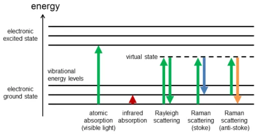
Raman scattering is a scattering process of photon with bonds. In most case, the scattering is elastic and results in Rayleigh scattering. However, if there is energy transfer in the process (i.e. inelastic scattering), the bond vibrational level would change, and the scattered photon would loss or gains the corresponding energy.7 The selection rule of this process is Δ 1 and Δ 0, 2 , where is rotational quantum number. The energy level diagram for a comparison of Raman scattering to other spectroscopic process is shown in Figure 1.
Figure 1 Energy level diagram of simple spectroscopic process. Drawn using MS Powerpoint with Figure 1 of Reference 8 as an example.
3
molecule. The magnitude of induced dipole is proportional to electrical polarizability of molecule. By considering the vibration as a combination of orthogonally normal vibration modes, the scattering effect on each vibration can be considered separately. The scattering process is often represented by this equation:7–9
2 1
2 2
1
2 2
where is the induced dipole moment, is polarizability, is the initial polarizability without vibration, is the electric field amplitude of photon, is frequency of photon, is frequency change after the scattering, is the position in normal coordinate of the vibration, and is the initial (middle) position in the coordinate of the vibration.
One can see that the photon frequency changes (i.e. energy transfer) only in the second
and third term. If the vibration does not change polarizability of molecule, the term
would be zero, and the second and third term would be disappeared, and there would be no energy transfer. Thus, the first term represent Rayleigh scattering (elastic). The second term where photon loss energy represent Stoke Raman scattering, while the third term represent anti-stoke Raman scattering. This criterion of polarizability change is useful to explain the reason that some vibrational modes appear in infrared absorption spectra, but not in Raman spectra.7–9
In practice, Raman spectroscopy is much less problematic when encountering sample with water content, comparing to infrared absorption spectroscopy. The optic setup for Raman spectroscopy also relatively easy since the electromagnetic wave in the process is in in visible Region. Raman spectroscopy have been used in many fields of research and industry, including but not limited to organic chemistry10–13, materials science14,15, biological
Diffraction Limit
Many modern Raman spectrometers (and also similar spectrometer such as IR, NIR) are equipped with microscope to acquire the signal from a small spot. Obviously, any simple aberrations of optical microscope (e.g. spherical aberration, coma, distortion, etc.) would also apply to the Raman spectrometer as well, and thus the quality of optic setup would limit the spatial resolution.29 Nevertheless, even with the ideal setup with minimal aberration, there is
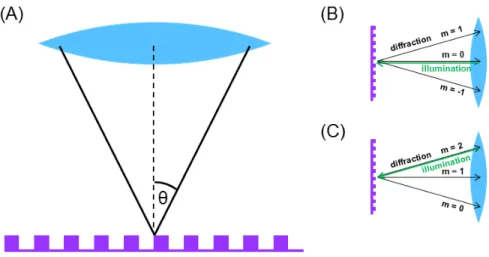
another barrier, which is the diffraction of light. Ernst Abbe in 1873 and Hermann von
Helmhotz in a year later made a mathematical approach of this limit using objective lens and grating (Figure 1).
Figure 2 Schema of the setup in Abby’s consideration of diffraction limit. Objective lens and grating (A), together with the consideration in the case of (B) perpendicular illumination and (C) angled illumination. Drawn using MS Powerpoint with Figure 4 of Reference 29 as an example.
Abbe argue that each unit of grating could be resolved by the microscope if one could detect the first diffraction maxima (aside from central maxima).30 When considering illumination perpendicular to grating plane (Figure 1B), the minimum grating spacing (d) which the first maxima can be detected is denoted by:
5
sin
where λ is the wavelength of the illumination, n is the refractive index of the objective lens, θ is the half angle of light cone, and NA is the numerical aperture of the objective lens.30 However, when considering angled illumination (Figure 1C), the smaller d can be acquired. When the same lens is used in both illumination and signal collection, the equation becomes the Abby’s formula of diffraction limit:
2
With 555 nm illumination and objective lens with 0.9 NA, the diffraction limit is about 308 nm, thus the practical diffraction limit around 300 nm previously stated.
Since the diffraction is a fundamental property of light waves, this limit cannot be overcome with conventional setup of optical parts. No matter how much the magnification is, the detail of samples smaller than this limit cannot be resolved, and the output image just appears larger without additional details. The magnification beyond this useful point is often called ‘empty magnification’.31
In microscopy, this limit was easily surpassed by replacing light wave with electron. Electron wavelength in picometers scale can be attained by standard electron microscope.32 However, in Raman spectroscopy, the wavelength around visible region is needed, and thus other methods are required to break through this limit and achieve nanoscale characterization of material with Raman spectroscopy.
Super-resolution Raman spectroscopy
are to increase NA of objective lens and decrease wavelength. High-NA objectives lens are commercially available in the form of oil-immersion lens, with NA as high as 1.4 being very feasible. The use of high NA lens is a basic which can be combined with following resolution-improving technique.33–35 The other basic pathway, decreasing wavelength, have been realized
in UV-Raman. With the smaller wavelength of ultraviolet light, a spatial resolution of 150 nm was demonstrated.35 Attenuated total reflection (ATR) mode Raman spectroscopy also reduces
wavelength of visible excitation laser by using high refractive index medium such as ZnSe (n = 2.6), and thus improving spatial resolution.36 It should be mentioned that although UV and
ATR Raman spectroscopy can improve spatial resolution, it is not the main purpose of the techniques. Ultraviolet excitation allows resonance Raman effect for samples with high energy gap between electronic ground state and excitation state (e.g. polycyclic aromatic hydrocarbon and amino acids).37 ATR mode penetrates only small depth from surface of the sample, allowing surface and interface study.36
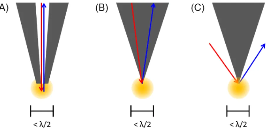
To further improve the spatial resolution, near-field techniques were utilized.38 By placing the illumination or collection very close to the probing spot, diffraction can be restrained. A notable method without using complex mechanism is to use dielectric microsphere as a near-field lens, which demonstrates the Raman measurement with spatial resolution of 80 nm.39 Scanning near-field optical microscopy (SNOM), also called as Near field scanning optical microscopy (NSOM) is one of the few techniques which provide spatial resolution for Raman spectroscopy down to single molecular level.40,41 The principle of SNOM is to utilize the nanoscale manipulation capability of scanning probe microscopy (SPM) such as scanning tunneling microscopy (STM) or atomic force microscope (AFM) by control tips with nanometers size apex to the target, then use the geometry of the tips to confine probing area of optical microscope.40–44 Figure 2 presents a basic view of SNOM, the
diffracted light is blocked (in the case of aperture SNOM) or prevented from the light path (ATR SNOM or scattering SNOM).
7
Figure 3 Examples of typical setups of SNOM. (A) Aperture SNOM, (B) ATR SNOM, and (C) scattering SNOM. Noted that the SNOM approach can be used in just illumination, just collection, or both. Drawn with MS Powerpoint using explanation from Reference 39-43.
By mostly eliminate the effects from diffraction, the spatial resolution is improved dramatically. SNOM based Raman spectroscopy have been used to perform nanoscale characterizations of human cells45, fossils46, damaged silicon wafer47, CVD-diamond layers48, and carbon nanomaterials49, all with spatial resolutions of 100 nm or better. SNOM can be used with other microscopy and spectroscopy as well as Raman.40,41
Localized surface plasmon resonance (LSPR) is an interaction between electron cloud in material and electric field of incoming light wave.50 For electromagnetic wave in visible region, LSPR is easily achievable by nanoparticles/nanostructure of noble metal such as silver and gold.50 LSPR produces two important effects to this topic, immense enhancement in nanoscale distance from the metal surface50,51 and wavelength contraction52, both effects, with proper environment, can greatly improve spatial resolution in Raman measurement.1,3,53 The plasmon resonance enhancement-assisted Raman spectroscopy is the basic of surface enhance Raman scattering spectroscopy (SERS), while scattering SNOM with SERS is the principle of tip-enhanced Raman scattering spectroscopy (TERS). These two techniques are the main focus of this thesis. With TERS, spatial resolution down to few nanometers or even sub-nanometers is feasible.54–58
Raman spectroscopy. For example, visible/IR optical microscopy with spatial resolution of 10 nm was demonstrated.59,60
Surface-enhanced Raman scattering spectroscopy (SERS)
Surface-enhanced Raman scattering spectroscopy is a technique which relies on an enhancement effect when target molecule is in a vicinity of certain materials. There are two mechanism which is involved in Raman signal enhancement, electromagnetic enhancement mechanism and chemical enhancement mechanism.61 The materials which can enhance the
Raman signal are called SERS substrate. Since the enhancement can be as high as million to billion times, SERS allows ultrasensitive detection of chemical and biological substance. Trace contaminant with concentration as low as 10-15 M can be detected using SERS.62 Trinitrotoluene (TNT)63, DNA64, mercury65, and proteins66 with concentration in nanomolar to attomolar range can be detected using SERS.
Fleischmann, Hendra and McQuillan observed SERS effect on 1974, but they explained as it was high surface area that provided unusually high Raman signal of pyridine on unsmooth silver substrate.67,68 Jeanmaire and Van Duyne69, and also Albrecht and Creighton70 later clarified that the high signal was a result of electric field enhancement by silver structure. The origin of electric field enhancement is LSPR between light and electron cloud in metal nanostructure as explained in the previous section. SERS was solely explained by electromagnetic enhancement mechanism until the discovery of chemical enhancement mechanism.71–73 Some molecules have been found to have 10-1000 times enhancement factor compare to the others, and this phenomenon is substrate dependent, such as pyridine and piperidine on silver.74 The process of chemical enhancement mechanism is explain as when
molecules adsorbed on a substrate, charge-transfer between energy level of molecules and the substrate is possible via Herzberg-Teller vibronic coupling. This allows a resonance Raman-like effect, which enhance scattering signal.61,74 This mechanism allows SERS effect on other
9
The magnitude of LSPR electric enhancement around spherical metallic nanoparticle can be represent by the equation50,76:
, , ̂
2
̂ 3
̂
where is the enhanced electric field vector, is the magnitude of electric field of incoming photon, is complex dielectric constant of metal, is complex dielectric constant of the surrounding medium, is particle size, x, y, and z is position in the corresponding axis, and , , and ̂ is unit vector in the corresponding axis.
This equation provides many useful physical meanings. First, if the real part of is close to 2 and its imaginary part is near-zero, the 2 in the denominator would approaches zero, resulting in extremely high value of the overall term. This is possible in the case when the particle is silver or gold, as the two metals provide negative real part of dielectric constant in visible wavelength region. Since dielectric constant is highly dependent on wavelength, only small region of wavelength would give near-zero 2 value and extreme field enhancement. This is the background of the word “resonance” in the process name. For small metal particle in water, the resonance wavelength is around 400 nm for silver and 520 nm for gold. Second, enhancement from LSPR is strongly geometry dependent. The size of particle has power of 3 in the equation. The shape of particle also crucial because the form of the equation would change drastically in the case of non-spherical particles. Third, the term and in the denominator indicate the field enhancement is very strong near the particle surface and is quickly weaken as the distance from the particle increases.
Since LSPR is highly localized and SERS signal is immensely high compared to normal Raman scattering, the signal from sample within small area of enhanced electric field can overwhelm the signal from neighbor area. This spot is called “hot spot”.76,77 This effect
can provide a very high spatial resolution if the exact position of hot spot is known. However, even though SERS can provide Raman signal from spot smaller than diffraction limit, if there are many hot spot together in large groups, diffraction limit cannot be exceeded because the signal is an average from spots over a large area. Moreover, even in the case of SERS with single nanoparticle (i.e. single hot spot), if the precise position of the particle is not certain, one need to do SERS mapping to find the position. In this case, hot spot would appear as large as diffraction limit because Abby’s criterion also applies for self-luminous sample.30 In order
to realize and control the position of hotspot, SERS probe can be attached to SPM, and this is the origin of TERS.
There are studies of using SERS to get improved spatial resolution. Tracking of free-floating gold nanoparticles in cells and repeating SERS measurement provides Raman spectra of intracellular pathway.78 In Chapter 3 of this thesis, SERS effect is used to improved spatial resolution in Z axis, which is a problem for Raman spectroscopy within polymers. These two studies achieve good spatial resolution, but not surpassing diffraction limit.
Tip-enhanced Raman scattering spectroscopy (TERS)
TERS is a combination of SERS and SNOM, but SERS substrate in a form of nanotips connected to SPM instrument is used instead of nanoparticles/nanostructure under samples. As in SERS, the Raman signal enhancement arises from near-field enhancement of electric field via LSPR interaction between metallic nanostructures and incident light. In the case of TERS, the nanostructures are nano-sized apex of metallic tip. From the equation of LSPR near-field enhancement, one can see that the enhancement is very strong in the small distance near the enhancing surface, but decrease drastically as the distance increase. Thus, enhancement by nanotips is confined to the small volume at the tip apex. ‘Lighting rod effect’ also contributes to the electric field enhancement and confinement at the tip apex.79 Due to the confinement, this enhancement can provide SERS signal with nanoscale spatial resolution,
11
exceeding diffraction limit of light. Resolution of 1.7 nm can archived in ambient condition (room temperature, normal pressure).54 With ultrahigh vacuum and low temperature, even subnanometer resolution is possible.
Since the enhancement mechanism of TERS is the same as SERS, all principle of SERS also applies. The material of the tip must be compatible with the wavelength of incident laser. For example, silver tips are normally used in TERS experiment with 514 nm or 532 nm excitation lasers while gold tips are compatible with laser wavelength in the region of 600-700 nm (often 632.8 nm helium-neon laser). Topology of tips also drastically affects the enhancement factor.80,81
An advantage of TERS is that it provides both topological information from SPM and molecular vibration from Raman spectroscopy. The correlation between the two information is highly valuable for nanomaterial characterization. With the exceeding spatial resolution, TERS have been used to study nanoscale photocatalytic reaction82, sub-molecular photochemistry57, adsorbed species on single-crystal surface83, and nanomaterial such as GaN nanowires1, nanotransistors84, polymer nanocomposite27,85, carbon nanotube3,54,86–88, and graphene34,89–100.
In practice, TERS experiments come with various setup and instrumentation. The illumination mode can be from top, side, or bottom. The tip control scheme can be AFM, which is compatible with almost all sample, or STM, which can adjust tip-sample distance. The material of the tip can be gold for chemical stability or silver for slightly higher enhancement. Tip can also be etched bulk metal tip or metal-coated AFM tip. A notable setup is gap mode TERS, which is performed by placing the sample on SERS-active substrate (usually gold or silver flim) and position TERS tip on the top. The gap created by the tip and substrate provides additional enhancement about 100 times to TERS signal.1,53,86 Figure 4
represent electric field enhancement in gap-mode TERS from finite-difference time-domain calculation with 40 nm tip apex, 3 nm silver tip-silver plate distance, and 514 nm excitation wavelength.
Figure 4 FDTD calculation showing electric field enhancement in gap-mod TERS
Recent advances in TERS development includes low-temperature low-pressure TERS57,101, which significantly reduce the problem from thermal drift, high-enhancement advance tips such as rough surface tips80 and bowtie nanoantenna tip with self-producing gap mode81, synchronize tip tapping- Raman measurement which allows near-field and far-field measurement in a single run33, Wave-guided tip102, pressure-assisted TERS56, and electrochemical TERS103,104.
The studies in this thesis do not involved in the development of TERS, but an application of TERS in a characterization of nanomaterial was demonstrated. In Chapter 1, TERS was used to reveal the properties and formation mechanism of nanostructures on epitaxial graphene. In Chapter 2, similar structures were studied, but on graphene micoisland, which allows a further discussion of established and alternate mechanism for nanostructures formation.
Grapene and graphene nanostructure
Graphene is a novel nanometerials with a large number of unique and interesting properties. Graphene have been shown to have zero band gap105,106, tunable band gap107,108, quantum hall
13
effects109,110, ballistic transport111, extremely high tensile strength and Young’s modulus112, Raman enhancement capability113–115, large surface area116, transparency117, etc. Due to these impressive properties, graphene have been demonstrate to be a promising material in high-speed electronics116, ultrafast photodetector118, very high-frequency transistor119, and
supercapacitor120–122.
In order to build high-quality graphene device, a production of large amount of high-quality graphene sheet is a crucial key factor. The most well-known method for graphene synthesis, the “scotch tape” exfoliation of highly ordered pyrolysis graphene provide graphene sheet with minimal defect, but it can only produce small flake of graphene.111,123 Scotch tape peeling also require a lot of manual labor which is difficult to practice in large-scale. The liquid oxidation exfoliation method convert graphite into graphite oxide, cleaving between the flakes of graphene oxide and then reduces them back into graphene.124–126 This method can produces large number of graphene sheet but contains large amount of defects. Chemical vapor deposition of methane on metal and on-SiC epitaxial growth can produce low-defect, wafer-size graphene sheet. Both method can also easily scale up to mass scale. However, epitaxial-grown graphene has an advantage over CVD graphene, as SiC is an electrical insulator. Thus, graphene grown on SiC does not need a substrate transfer process to be used in electric circuit.
TERS have been used to characterize graphene in nanoscale level. Number of layers34,92–
94,96,98, defects91,95, stress change28, Raman modes suppression97, edges99,100, and deposited
foreign chemical of graphene89,90,127 have all been investigated with great spatial resolution. However, before the studies in this thesis, there is no TERS study on important nanostructures of graphene such as nanoridges and nanosteps.
The instrument used in TERS studies in this thesis is special and very suitable for nanostructures study, as it control TERS tip by non-contact mode AFM. STM-TERS is not suitable for this study because undoped SiC is not conductive. TERS measurement of the structures by contact or tapping mode AFM TERS is also disputable because tip-graphene
interaction might interfere the true nature of graphene.
References
(1) Domke, K. F.; Pettinger, B. Studying Surface Chemistry beyond the Diffraction Limit: 10 Years of TERS. ChemPhysChem 2010, 11 (7), 1365–1373.
(2) Everall, N. J. Confocal Raman Microscopy: Why the Depth Resolution and Spatial Accuracy Can Be Much Worse than You Think. Appl. Spectrosc. 2000, 54 (10), 1515–1520.
(3) Verma, P.; Ichimura, T.; Yano, T.; Saito, Y.; Kawata, S. Nano-Imaging through Tip-Enhanced Raman Spectroscopy: Stepping beyond the Classical Limits. Laser Photonics Rev. 2009, 4 (4), 548–561. (4) Miller, F. A.; Mayo, D. W.; Hannah, R. W. Course Notes on the Interpretation of Infrared and
Raman Spectra; Wiley-Interscience: Hoboken, N.J, 2004.
(5) Larkin, P. Infrared and Raman Spectroscopy: Principles and Spectral Interpretation; Elsevier: Amsterdam ; Boston, 2011.
(6) Emerging Raman Applications and Techniques in Biomedical and Pharmaceutical Fields; Morris,
M. D., Matousek, P., Eds.; Biological and medical physics, biomedical engineering; Springer: Heidelburg ; New York, 2010.
(7) Li, Z.; Deen, M. J.; Kumar, S.; Selvaganapathy, P. R. Raman Spectroscopy for In-Line Water Quality Monitoring—Instrumentation and Potential. Sensors 2014, 14 (9), 17275–17303.
(8) Ferraro, J. R.; Nakamoto, K.; Brown, C. W. Chapter 1 - Basic Theory. In Introductory Raman
Spectroscopy (Second Edition); Academic Press: San Diego, 2003; pp 1–94.
(9) Albrecht, A. C. On the Theory of Raman Intensities. J. Chem. Phys. 1961, 34 (5), 1476–1484. (10) Socrates, G. Infrared and Raman Characteristic Group Frequencies: Tables and Charts, 3. ed., repr.
as paperback.; Wiley: Chichester, 2010.
(11) Dollish, F. R.; Fateley, W. G.; Bentley, F. F. Characteristic Raman Frequencies of Organic
Compounds; Wiley, 1974.
(12) Lin-Vien, D.; Colthup, N. B.; Fateley, W. G.; Grasselli, J. G. The Handbook of Infrared and Raman
Characteristic Frequencies of Organic Molecules; Elsevier, 1991.
(13) Nyquist, R. A.; Kagel, R. O. Handbook of Infrared and Raman Spectra of Inorganic Compounds
and Organic Salts: Infrared Spectra of Inorganic Compounds; Academic Press, 2012.
(14) Weber, W. H.; Merlin, R. Raman Scattering in Materials Science; Springer Science & Business Media, 2013.
(15) Cantarero, A. Raman Scattering Applied to Materials Science. Procedia Mater. Sci. 2015, 9, 113– 122.
(16) Peticolas, W. L. Applications of Raman Spectroscopy to Biological Macromolecules. Biochimie
1975, 57 (4), 417–428.
(17) Rae, A.; Stosch, R.; Klapetek, P.; Hight Walker, A. R.; Roy, D. State of the Art Raman Techniques for Biological Applications. Methods 2014, 68 (2), 338–347.
(18) Ayas, S.; Cinar, G.; Ozkan, A. D.; Soran, Z.; Ekiz, O.; Kocaay, D.; Tomak, A.; Toren, P.; Kaya, Y.; Tunc, I.; et al. Label-Free Nanometer-Resolution Imaging of Biological Architectures through Surface Enhanced Raman Scattering. Sci. Rep. 2013, 3.
(19) Smitthipong, W.; Gadiou, R.; Vidal, L.; Wagner, P.; Nardin, M. 3D Raman Images of Rubber Blends (IR–HNBR). Vib. Spectrosc. 2008, 46 (1), 8–13.
(20) Furukawa, T.; Sato, H.; Murakami, R.; Zhang, J.; Noda, I.; Ochiai, S.; Ozaki, Y. Raman Microspectroscopy Study of Structure, Dispersibility, and Crystallinity of Poly(hydroxybutyrate)/poly(l-Lactic Acid) Blends. Polymer 2006, 47 (9), 3132–3140.
(21) Tabaksblat, R.; Meier, R. J.; Kip, B. J. Confocal Raman Microspectroscopy: Theory and Application to Thin Polymer Samples. Appl. Spectrosc. 1992, 46 (1), 60–68.
(22) Malard, L. M.; Pimenta, M. A.; Dresselhaus, G.; Dresselhaus, M. S. Raman Spectroscopy in Graphene. Phys. Rep. 2009, 473 (5-6), 51–87.
(23) Gupta, A.; Chen, G.; Joshi, P.; Tadigadapa, S.; Eklund. Raman Scattering from High-Frequency Phonons in Supported N-Graphene Layer Films. Nano Lett. 2006, 6 (12), 2667–2673.
(24) Ferrari, A. C.; Meyer, J. C.; Scardaci, V.; Casiraghi, C.; Lazzeri, M.; Mauri, F.; Piscanec, S.; Jiang, D.; Novoselov, K. S.; Roth, S.; et al. Raman Spectrum of Graphene and Graphene Layers. Phys.
Rev. Lett. 2006, 97 (18), 187401.
(25) Ni, Z. H.; Chen, W.; Fan, X. F.; Kuo, J. L.; Yu, T.; Wee, A. T. S.; Shen, Z. X. Raman Spectroscopy of Epitaxial Graphene on a SiC Substrate. Phys. Rev. B 2008, 77 (11), 115416.
15
(26) Schmidt, D. A.; Ohta, T.; Beechem, T. E. Strain and Charge Carrier Coupling in Epitaxial Graphene.
Phys. Rev. B 2011, 84 (23), 235422.
(27) Yan, X.; Suzuki, T.; Kitahama, Y.; Sato, H.; Itoh, T.; Ozaki, Y. A Study on the Interaction of Single-Walled Carbon Nanotubes (SWCNTs) and Polystyrene (PS) at the Interface in SWCNT–PS Nanocomposites Using Tip-Enhanced Raman Spectroscopy. Phys. Chem. Chem. Phys. 2013, 15 (47), 20618–20624.
(28) Suzuki, T.; Itoh, T.; Vantasin, S.; Minami, S.; Kutsuma, Y.; Ashida, K.; Kaneko, T.; Morisawa, Y.; Miura, T.; Ozaki, Y. Tip-Enhanced Raman Spectroscopic Measurement of Stress Change in the Local Domain of Epitaxial Graphene on the Carbon Face of 4H-SiC(0001¯). Phys. Chem. Chem.
Phys. 2014, 16 (37), 20236–20240.
(29) Booth, M. J. Adaptive Optical Microscopy: The Ongoing Quest for a Perfect Image. Light Sci. Appl.
2014, 3 (4), e165.
(30) Weisenburger, S.; Sandoghdar, V. Light Microscopy: An Ongoing Contemporary Revolution.
Contemp. Phys. 2015, 56 (2), 123–143.
(31) Heintzmann, R.; Ficz, G. Breaking the Resolution Limit in Light Microscopy. Brief. Funct.
Genomic. Proteomic. 2006, 5 (4), 289–301.
(32) Freitag, B.; Kujawa, S.; Mul, P. M.; Ringnalda, J.; Tiemeijer, P. C. Breaking the Spherical and Chromatic Aberration Barrier in Transmission Electron Microscopy. Ultramicroscopy 2005, 102 (3), 209–214.
(33) Yu, J.; Saito, Y.; Ichimura, T.; Kawata, S.; Verma, P. Far-Field Free Tapping-Mode Tip-Enhanced Raman Microscopy. Appl. Phys. Lett. 2013, 102 (12), 123110.
(34) Saito, Y.; Verma, P.; Masui, K.; Inouye, Y.; Kawata, S. Nano-Scale Analysis of Graphene Layers by Tip-Enhanced near-Field Raman Spectroscopy. J. Raman Spectrosc. 2009, 40 (10), 1434–1440. (35) Poborchii, V.; Tada, T.; Kanayama, T. Study of Stress in a Shallow-Trench-Isolated Si Structure
Using Polarized Confocal near-UV Raman Microscopy of Its Cross Section. Appl. Phys. Lett. 2007,
91 (24), 241902.
(36) Tisinger, L. G.; Sommer, A. J. Attenuated Total Internal Reflection (ATR) Raman Microspectroscopy. Microsc. Microanal. 2004, null (Supplement S02), 1318–1319.
(37) Asher, S. A. Ultraviolet Raman Spectrometry. In Handbook of Vibrational Spectroscopy; John Wiley & Sons, Ltd, 2006.
(38) Zheng, X.; Zong, C.; Xu, M.; Wang, X.; Ren, B. Raman Imaging from Microscopy to Nanoscopy, and to Macroscopy. Small 2015, 11 (28), 3395–3406.
(39) Kasim, J.; Ting, Y.; Meng, Y. Y.; Ping, L. J.; See, A.; Jong, L. L.; Xiang, S. Z. Near-Field Raman Imaging Using Optically Trapped Dielectric Microsphere. Opt. Express 2008, 16 (11), 7976–7984. (40) Lereu, A. l.; Passian, A.; Dumas, P. Near Field Optical Microscopy: A Brief Review. Int. J.
Nanotechnol. 2012, 9 (3-7), 488–501.
(41) Saiki, T. Recent Advances in near-Field Optical Microscopy. In Microprocesses and
Nanotechnology Conference, 2002. Digest of Papers. Microprocesses and Nanotechnology 2002. 2002 International; 2002; pp 6–7.
(42) Futamata, M.; Bruckbauer, A. ATR-SNOM-Raman Spectroscopy. Chem. Phys. Lett. 2001, 341 (5– 6), 425–430.
(43) Jahncke, C. L.; Paesler, M. A.; Hallen, H. D. Raman Imaging with Near‐field Scanning Optical Microscopy. Appl. Phys. Lett. 1995, 67 (17), 2483–2485.
(44) Gouadec, G.; Colomban, P. Raman Spectroscopy of Nanomaterials: How Spectra Relate to Disorder, Particle Size and Mechanical Properties. Prog. Cryst. Growth Charact. Mater. 2007, 53 (1), 1–56.
(45) Schaller, R. D.; Ziegelbauer, J.; Lee, L. F.; Haber, L. H.; Saykally, R. J. Chemically Selective Imaging of Subcellular Structure in Human Hepatocytes with Coherent Anti-Stokes Raman Scattering (CARS) Near-Field Scanning Optical Microscopy (NSOM). J. Phys. Chem. B 2002, 106 (34), 8489–8492.
(46) Kaupp, G. Scanning near-Field Optical Microscopy on Rough Surfaces: Applications in Chemistry, Biology, and Medicine. Int. J. Photoenergy 2006, 2006, e69878.
(47) Webster, S.; Smith, D. A.; Batchelder, D. N. Raman Microscopy Using a Scanning near-Field Optical Probe. Vib. Spectrosc. 1998, 18 (1), 51–59.
(48) Goetz, M.; Drews, D.; Zahn, D. R. T.; Wannemacher, R. Near-Field Raman Spectroscopy of Semiconductor Heterostructures and CVD-Diamond Layers. J. Lumin. 1998, 76–77, 306–309. (49) Grosse, K. Nanometer-Scale Temperature Measurements of Phase Change Memory and Carbon
Nanomaterials, University of Illinois: Urbana, Illinois, 2014.
(50) Willets, K. A.; Duyne, R. P. V. Localized Surface Plasmon Resonance Spectroscopy and Sensing.
(51) Richards, D.; Milner, R. G.; Huang, F.; Festy, F. Tip-Enhanced Raman Microscopy: Practicalities and Limitations. J. Raman Spectrosc. 2003, 34 (9), 663–667.
(52) Douillard, L.; Charra, F.; Korczak, Z.; Bachelot, R.; Kostcheev, S.; Lerondel, G.; Adam, P.-M.; Royer, P. Short Range Plasmon Resonators Probed by Photoemission Electron Microscopy. Nano
Lett. 2008, 8 (3), 935–940.
(53) Kawata, S.; Inouye, Y.; Verma, P. Plasmonics for near-Field Nano-Imaging and Superlensing. Nat.
Photonics 2009, 3 (7), 388–394.
(54) Chen, C.; Hayazawa, N.; Kawata, S. A 1.7 Nm Resolution Chemical Analysis of Carbon Nanotubes by Tip-Enhanced Raman Imaging in the Ambient. Nat. Commun. 2014, 5, 3312.
(55) Ichimura, T.; Fujii, S.; Verma, P.; Yano, T.; Inouye, Y.; Kawata, S. Subnanometric Near-Field Raman Investigation in the Vicinity of a Metallic Nanostructure. Phys. Rev. Lett. 2009, 102 (18), 186101. (56) Yano, T.; Verma, P.; Saito, Y.; Ichimura, T.; Kawata, S. Pressure-Assisted Tip-Enhanced Raman
Imaging at a Resolution of a Few Nanometres. Nat. Photonics 2009, 3 (8), 473–477.
(57) Zhang, R.; Zhang, Y.; Dong, Z. C.; Jiang, S.; Zhang, C.; Chen, L. G.; Zhang, L.; Liao, Y.; Aizpurua, J.; Luo, Y.; et al. Chemical Mapping of a Single Molecule by Plasmon-Enhanced Raman Scattering.
Nature 2013, 498 (7452), 82–86.
(58) Pettinger, B. Single-Molecule Surface- and Tip-Enhanced Raman Spectroscopy. Mol. Phys. 2010,
108 (16), 2039–2059.
(59) Cvitkovic, A.; Ocelic, N.; Hillenbrand, R. Material-Specific Infrared Recognition of Single Sub-10 Nm Particles by Substrate-Enhanced Scattering-Type Near-Field Microscopy. Nano Lett. 2007, 7 (10), 3177–3181.
(60) Hillenbrand, R.; Keilmann, F. Material-Specific Mapping of Metal/semiconductor/dielectric Nanosystems at 10 Nm Resolution by Backscattering near-Field Optical Microscopy. Appl. Phys.
Lett. 2002, 80 (1), 25–27.
(61) Ji, W.; Spegazzini, N.; Kitahama, Y.; Chen, Y.; Zhao, B.; Ozaki, Y. pH-Response Mechanism of P-Aminobenzenethiol on Ag Nanoparticles Revealed By Two-Dimensional Correlation Surface-Enhanced Raman Scattering Spectroscopy. J. Phys. Chem. Lett. 2012, 3 (21), 3204–3209.
(62) Yang, S.; Dai, X.; Stogin, B. B.; Wong, T.-S. Ultrasensitive Surface-Enhanced Raman Scattering Detection in Common Fluids. Proc. Natl. Acad. Sci. 2016, 113 (2), 268–273.
(63) He, X.; Wang, H.; Li, Z.; Chen, D.; Liu, J.; Zhang, Q. Ultrasensitive SERS Detection of Trinitrotoluene through Capillarity-Constructed Reversible Hot Spots Based on ZnO–Ag Nanorod Hybrids. Nanoscale 2015, 7 (18), 8619–8626.
(64) Fan, Z.; Kanchanapally, R.; Ray, P. C. Hybrid Graphene Oxide Based Ultrasensitive SERS Probe for Label-Free Biosensing. J. Phys. Chem. Lett. 2013, 4 (21), 3813–3818.
(65) Xu, L.; Yin, H.; Ma, W.; Kuang, H.; Wang, L.; Xu, C. Ultrasensitive SERS Detection of Mercury Based on the Assembled Gold Nanochains. Biosens. Bioelectron. 2015, 67, 472–476.
(66) Zhao, S.; Ma, W.; Xu, L.; Wu, X.; Kuang, H.; Wang, L.; Xu, C. Ultrasensitive SERS Detection of VEGF Based on a Self-Assembled Ag ornamented–AU Pyramid Superstructure. Biosens.
Bioelectron. 2015, 68, 593–597.
(67) Surface-Enhanced Raman Scattering; Kneipp, K., Moskovits, M., Kneipp, H., Eds.; Topics in Applied Physics; Springer Berlin Heidelberg, 2006; Vol. 103.
(68) McQuillan, A. J. The Discovery of Surface-Enhanced Raman Scattering. Notes Rec. R. Soc. 2009,
63 (1), 105–109.
(69) Jeanmaire, D. L.; Van Duyne, R. P. Surface Raman Spectroelectrochemistry. J. Electroanal. Chem.
Interfacial Electrochem. 1977, 84 (1), 1–20.
(70) Albrecht, M. G.; Creighton, J. A. Anomalously Intense Raman Spectra of Pyridine at a Silver Electrode. J. Am. Chem. Soc. 1977, 99 (15), 5215–5217.
(71) Burstein, E.; Chen, Y. J.; Chen, C. Y.; Lundquist, S.; Tosatti, E. “Giant” Raman Scattering by Adsorbed Molecules on Metal Surfaces. Solid State Commun. 1979, 29 (8), 567–570.
(72) Persson, B. N. J. On the Theory of Surface-Enhanced Raman Scattering. Chem. Phys. Lett. 1981, 82 (3), 561–565.
(73) Gersten, J. I.; Birke, R. L.; Lombardi, J. R. Theory of Enhance I Light Scattering from Molecules Adsorbed at the Metal-Solution Interface. Phys. Rev. Lett. 1979, 43 (2), 147–150.
(74) Lombardi, J. R.; Birke, R. L.; Lu, T.; Xu, J. Charge‐transfer Theory of Surface Enhanced Raman Spectroscopy: Herzberg–Teller Contributions. J. Chem. Phys. 1986, 84 (8), 4174–4180.
(75) Lombardi, J. R.; Birke, R. L. Theory of Surface-Enhanced Raman Scattering in Semiconductors. J.
Phys. Chem. C 2014, 118 (20), 11120–11130.
(76) Le Ru, E. C.; Etchegoin, P. G. Principles of Surface-Enhanced Raman Spectroscopy: And Related
Plasmonic Effects, 1st ed.; Elsevier: Amsterdam ; Boston, 2009.
17 sciences; Springer: Dordrecht, 2007.
(78) Huang, K.-C.; Bando, K.; Ando, J.; Smith, N. I.; Fujita, K.; Kawata, S. 3D SERS (surface Enhanced Raman Scattering) Imaging of Intracellular Pathways. Methods 2014, 68 (2), 348–353.
(79) Asghari-Khiavi, M.; Wood, B. R.; Hojati-Talemi, P.; Downes, A.; McNaughton, D.; Mechler, A. Exploring the Origin of Tip-Enhanced Raman Scattering; Preparation of Efficient TERS Probes with High Yield. J. Raman Spectrosc. 2012, 43 (2), 173–180.
(80) Taguchi, A.; Yu, J.; Verma, P.; Kawata, S. Optical Antennas with Multiple Plasmonic Nanoparticles for Tip-Enhanced Raman Microscopy. Nanoscale 2015, 7 (41), 17424–17433.
(81) Schuck, P. J.; Weber-Bargioni, A.; Ashby, P. D.; Ogletree, D. F.; Schwartzberg, A.; Cabrini, S. Life Beyond Diffraction: Opening New Routes to Materials Characterization with Next-Generation Optical Near-Field Approaches. Adv. Funct. Mater. 2013, 23 (20), 2539–2553.
(82) Kumar, N.; Stephanidis, B.; Zenobi, R.; Wain, A. J.; Roy, D. Nanoscale Mapping of Catalytic Activity Using Tip-Enhanced Raman Spectroscopy. Nanoscale 2015, 7 (16), 7133–7137.
(83) Wang, X.; Liu, Z.; Zhuang, M.-D.; Zhang, H.-M.; Wang, X.; Xie, Z.-X.; Wu, D.-Y.; Ren, B.; Tian, Z.-Q. Tip-Enhanced Raman Spectroscopy for Investigating Adsorbed Species on a Single-Crystal Surface Using Electrochemically Prepared Au Tips. Appl. Phys. Lett. 2007, 91 (10), 101105. (84) Tarun, A.; Hayazawa, N.; Kawata, S. Tip-Enhanced Raman Spectroscopy for Nanoscale Strain
Characterization. Anal. Bioanal. Chem. 2009, 394 (7), 1775–1785.
(85) Suzuki, T.; Yan, X.; Kitahama, Y.; Sato, H.; Itoh, T.; Miura, T.; Ozaki, Y. Tip-Enhanced Raman Spectroscopy Study of Local Interactions at the Interface of Styrene–Butadiene Rubber/Multiwalled Carbon Nanotube Nanocomposites. J. Phys. Chem. C 2013, 117 (3), 1436–1440.
(86) Kawata, S.; Verma, P. Optical Nano-Imaging of Materials: Peeping Through Tip-Enhanced Raman Scattering. Chim. Int. J. Chem. 2006, 60 (11), 770–776.
(87) Yano, T.; Ichimura, T.; Kuwahara, S.; H’Dhili, F.; Uetsuki, K.; Okuno, Y.; Verma, P.; Kawata, S. Tip-Enhanced Nano-Raman Analytical Imaging of Locally Induced Strain Distribution in Carbon Nanotubes. Nat. Commun. 2013, 4.
(88) Chaunchaiyakul, S.; Yano, T.; Khoklang, K.; Krukowski, P.; Akai-Kasaya, M.; Saito, A.; Kuwahara, Y. Nanoscale Analysis of Multiwalled Carbon Nanotube by Tip-Enhanced Raman Spectroscopy.
Carbon 2016, 99, 642–648.
(89) Xu, G.; Liu, Z.; Xu, K.; Zhang, Y.; Zhong, H.; Fan, Y.; Huang, Z. Constant Current Etching of Gold Tips Suitable for Tip-Enhanced Raman Spectroscopy. Rev. Sci. Instrum. 2012, 83 (10), 103708. (90) Poliani, E.; Nippert, F.; Maultzsch, J. Effect of Gap Modes on Graphene and Multilayer Graphene in
Tip-Enhanced Raman Spectroscopy. Phys. Status Solidi B 2012, 249 (12), 2511–2514.
(91) Rickman, R. H.; Dunstan, P. R. Enhancement of Lattice Defect Signatures in Graphene and Ultrathin Graphite Using Tip-Enhanced Raman Spectroscopy: Enhancement of Defect Signatures in Graphene Using Tip-Enhanced Raman. J. Raman Spectrosc. 2014, 45 (1), 15–21.
(92) Hoffmann, G. G.; Xue, L.; Loos, J.; de With, G. High-Resolution Tip-Enhanced Raman Mapping.
Macromol. Symp. 2011, 305 (1), 26–42.
(93) Hoffmann, G. G.; de With, G.; Loos, J. Micro-Raman and Tip-Enhanced Raman Spectroscopy of Carbon Allotropes. Macromol. Symp. 2008, 265 (1), 1–11.
(94) Snitka, V.; Rodrigues, R. D.; Lendraitis, V. Novel Gold Cantilever for Nano-Raman Spectroscopy of Graphene. Microelectron. Eng. 2011, 88 (8), 2759–2762.
(95) Wang, P.; Zhang, D.; Li, L.; Li, Z.; Zhang, L.; Fang, Y. Reversible Defect in Graphene Investigated by Tip-Enhanced Raman Spectroscopy. Plasmonics 2012, 7 (3), 555–561.
(96) Ghislandi, M.; Hoffmann, G. G.; Tkalya, E.; Xue, L.; With, G. D. Tip-Enhanced Raman Spectroscopy and Mapping of Graphene Sheets. Appl. Spectrosc. Rev. 2012, 47 (5), 371–381. (97) Domke, K. F.; Pettinger, B. Tip-Enhanced Raman Spectroscopy of 6H-SiC with Graphene Adlayers:
Selective Suppression of E1 Modes. J. Raman Spectrosc. 2009, 40 (10), 1427–1433.
(98) Pashaee, F.; Sharifi, F.; Fanchini, G.; Lagugné-Labarthet, F. Tip-Enhanced Raman Spectroscopy of Graphene-like and Graphitic Platelets on Ultraflat Gold Nanoplates. Phys. Chem. Chem. Phys.
2015, 17 (33), 21315–21322.
(99) Shiotari, A.; Kumagai, T.; Wolf, M. Tip-Enhanced Raman Spectroscopy of Graphene Nanoribbons on Au(111). J. Phys. Chem. C 2014, 118 (22), 11806–11812.
(100) Su, W.; Roy, D. Visualizing Graphene Edges Using Tip-Enhanced Raman Spectroscopy. J. Vac. Sci.
Technol. B 2013, 31 (4), 041808.
(101) Klingsporn, J. M.; Jiang, N.; Pozzi, E. A.; Sonntag, M. D.; Chulhai, D.; Seideman, T.; Jensen, L.; Hersam, M. C.; Duyne, R. P. V. Intramolecular Insight into Adsorbate–Substrate Interactions via Low-Temperature, Ultrahigh-Vacuum Tip-Enhanced Raman Spectroscopy. J. Am. Chem. Soc. 2014,
136 (10), 3881–3887.
Nanofocusing for Spectroscopy on the Nanoscale. J. Phys. Chem. Lett. 2012, 3 (7), 945–952. (103) Zeng, Z.-C.; Huang, S.-C.; Li, M.-H.; Huang, T.; Ren, B. Electrochemical Tip-Enhanced Raman
Spectroscopy (EC-TERS). Meet. Abstr. 2014, MA2014-03 (4), 497–497.
(104) Zeng, Z.-C.; Huang, S.-C.; Wu, D.-Y.; Meng, L.-Y.; Li, M.-H.; Huang, T.-X.; Zhong, J.-H.; Wang, X.; Yang, Z.-L.; Ren, B. Electrochemical Tip-Enhanced Raman Spectroscopy. J. Am. Chem. Soc.
2015, 137 (37), 11928–11931.
(105) Gui, G.; Li, J.; Zhong, J. Band Structure Engineering of Graphene by Strain: First-Principles Calculations. Phys. Rev. B 2008, 78 (7), 075435.
(106) Duplock, E. J.; Scheffler, M.; Lindan, P. J. D. Hallmark of Perfect Graphene. Phys. Rev. Lett. 2004,
92 (22), 225502.
(107) Low, T.; Guinea, F.; Katsnelson, M. I. Gaps Tunable by Electrostatic Gates in Strained Graphene.
Phys. Rev. B 2011, 83 (19), 195436.
(108) Ni, Z. H.; Yu, T.; Lu, Y. H.; Wang, Y. Y.; Feng, Y. P.; Shen, Z. X. Uniaxial Strain on Graphene: Raman Spectroscopy Study and Band-Gap Opening. ACS Nano 2008, 2 (11), 2301–2305.
(109) Jiang, Z.; Zhang, Y.; Tan, Y.-W.; Stormer, H. L.; Kim, P. Quantum Hall Effect in Graphene. Solid
State Commun. 2007, 143 (1–2), 14–19.
(110) Jobst, J.; Waldmann, D.; Speck, F.; Hirner, R.; Maude, D. K.; Seyller, T.; Weber, H. B. Quantum Oscillations and Quantum Hall Effect in Epitaxial Graphene. Phys. Rev. B 2010, 81 (19), 195434. (111) Novoselov, K. S.; Geim, A. K.; Morozov, S. V.; Jiang, D.; Zhang, Y.; Dubonos, S. V.; Grigorieva, I.
V.; Firsov, A. A. Electric Field Effect in Atomically Thin Carbon Films. Science 2004, 306 (5696), 666–669.
(112) Lee, C.; Wei, X.; Kysar, J. W.; Hone, J. Measurement of the Elastic Properties and Intrinsic Strength of Monolayer Graphene. Science 2008, 321 (5887), 385–388.
(113) Ling, X.; Xie, L.; Fang, Y.; Xu, H.; Zhang, H.; Kong, J.; Dresselhaus, M. S.; Zhang, J.; Liu, Z. Can Graphene Be Used as a Substrate for Raman Enhancement? Nano Lett. 2010, 10 (2), 553–561. (114) Ling, X.; Moura, L. G.; Pimenta, M. A.; Zhang, J. Charge-Transfer Mechanism in
Graphene-Enhanced Raman Scattering. J. Phys. Chem. C 2012, 116 (47), 25112–25118.
(115) Xu, W.; Mao, N.; Zhang, J. Graphene: A Platform for Surface-Enhanced Raman Spectroscopy.
Small 2013, 9 (8), 1206–1224.
(116) Allen, M. J.; Tung, V. C.; Kaner, R. B. Honeycomb Carbon: A Review of Graphene. Chem. Rev.
2010, 110 (1), 132–145.
(117) Blake, P.; Hill, E. W.; Castro Neto, A. H.; Novoselov, K. S.; Jiang, D.; Yang, R.; Booth, T. J.; Geim, A. K. Making Graphene Visible. Appl. Phys. Lett. 2007, 91 (6), 063124.
(118) Xia, F.; Mueller, T.; Lin, Y.; Valdes-Garcia, A.; Avouris, P. Ultrafast Graphene Photodetector. Nat.
Immunol. 2009, 4 (12), 839–843.
(119) Lin, Y.-M.; Dimitrakopoulos, C.; Jenkins, K. A.; Farmer, D. B.; Chiu, H.-Y.; Grill, A.; Avouris, P. 100-GHz Transistors from Wafer-Scale Epitaxial Graphene. Science 2010, 327 (5966), 662–662. (120) Liu, C.; Yu, Z.; Neff, D.; Zhamu, A.; Jang, B. Z. Graphene-Based Supercapacitor with an Ultrahigh
Energy Density. Nano Lett. 2010, 10 (12), 4863–4868.
(121) Wang, Y.; Shi, Z.; Huang, Y.; Ma, Y.; Wang, C.; Chen, M.; Chen, Y. Supercapacitor Devices Based on Graphene Materials. J. Phys. Chem. C 2009, 113 (30), 13103–13107.
(122) Le, L. T.; Ervin, M. H.; Qiu, H.; Fuchs, B. E.; Lee, W. Y. Graphene Supercapacitor Electrodes Fabricated by Inkjet Printing and Thermal Reduction of Graphene Oxide. Electrochem. Commun.
2011, 13 (4), 355–358.
(123) Das, A.; Pisana, S.; Chakraborty, B.; Piscanec, S.; Saha, S. K.; Waghmare, U. V.; Novoselov, K. S.; Krishnamurthy, H. R.; Geim, A. K.; Ferrari, A. C.; et al. Monitoring Dopants by Raman Scattering in an Electrochemically Top-Gated Graphene Transistor. Nat. Nanotechnol. 2008, 3 (4), 210–215. (124) Stankovich, S.; Dikin, D. A.; Piner, R. D.; Kohlhaas, K. A.; Kleinhammes, A.; Jia, Y.; Wu, Y.;
Nguyen, S. T.; Ruoff, R. S. Synthesis of Graphene-Based Nanosheets via Chemical Reduction of Exfoliated Graphite Oxide. Carbon 2007, 45 (7), 1558–1565.
(125) McAllister, M. J.; Li, J.-L.; Adamson, D. H.; Schniepp, H. C.; Abdala, A. A.; Liu, J.; Herrera-Alonso, M.; Milius, D. L.; Car, R.; Prud’homme, R. K.; et al. Single Sheet Functionalized Graphene by Oxidation and Thermal Expansion of Graphite. Chem. Mater. 2007, 19 (18), 4396–4404.
(126) Zhou, Y.; Bao, Q.; Tang, L. A. L.; Zhong, Y.; Loh, K. P. Hydrothermal Dehydration for the “Green” Reduction of Exfoliated Graphene Oxide to Graphene and Demonstration of Tunable Optical Limiting Properties. Chem. Mater. 2009, 21 (13), 2950–2956.
(127) Stadler, J.; Schmid, T.; Zenobi, R. Nanoscale Chemical Imaging of Single-Layer Graphene. ACS
Nano 2011, 5 (10), 8442–8448.
Chapter I: Tip-Enhanced Raman Scattering of the Local
Nanostructure of Epitaxial Graphene Grown on 4H-SiC (000 )
Abstract
Step, ridge, and crack sub-micro/nanostructures of epitaxial graphene on 4H-SiC (0001) were characterized using tip-enhanced Raman scattering (TERS) spectroscopy. The nanostructures were created during graphene synthesis due to a difference in the thermal expansion coefficient of graphene and SiC. These structures are a distinctive property of epitaxial graphene, together with other desirable properties, such as large graphene sheet and minimal defects. The results of this study illustrate that the exceptional spatial resolution of TERS allows spectroscopic measurements of individual nanostructures, a feat which normal Raman spectroscopy is not capable of. By analyzing TERS spectra, the change of local strain on the nanoridge and decreased graphene content in the sub-micrometer crack were detected. Using G' band positions in the TERS spectra, the strain difference between ridge center and flat area was calculated to be 1.6 × 10⁻³ and 5.8 × 10⁻⁴ for uniaxial and biaxial strain, respectively. This confirms the proposed mechanism in previous researches that nanoridges on epitaxial graphene form as a relief against compressive strain. With this study, we demonstrate that TERS is a powerful technique for the characterization of individual local nanostructures on epitaxial graphene.
Introduction
Graphene is considered as a future material for chemical sensors, biosensors, and electronic devices due to its outstanding properties including, but not limited to, tremendous carrier mobility and a unique band gap.1–4 Among various types of graphene, epitaxial graphene grown on SiC has garnered considerable attention because of its large sheet area, minimal defects, and the electrical insulation properties of SiC, which allow the application in electronic circuits without the need of substrate transfer processes.5,6 The transparency of SiC under visible light can also be advantageous in graphene-based opto-electronic device.7 Graphene grown on either face of SiC does have differing properties: while graphene grown on Si face (0001 face) of SiC attaches strongly to the SiC surface, graphene grown on the
C-21
face (0001 face) has a weaker attraction to the SiC substrate due to the presence a carbon buffer layer.8 This allows some unique features of graphene on C face to occur, such as stack disordering of multilayer graphene, which allows extremely high mobility and unique nanostructures on the graphene sheet, which alters physical and electronic properties.9 It has been known that nanostructures can affect band gap10, electron mobility11, and internal strain12 of graphene. Therefore, it is possible to use strain engineering to control and manipulate the nanostructures and produce interesting products such as large band gap graphene.13
To characterize nanostructures of graphene grown on C-face and understand their forming mechanism, many groups have used atomic force microscopy (AFM)12, scanning
tunneling microscope (STM)11,14,15, and angle-resolved photoemission spectroscopy (ARPES)16 to study the morphology, occurrence frequency, synthesis temperature dependence, and effects on band structure of the most common nanostructures, e.g. ridges and steps. Among several techniques, Raman spectroscopy is considered as an ideal technique for graphene characterization because it provides robust information about defects17–21, internal strain22–26, stacking configuration27,28, number of layers27,29–32, and doping7,24,33. There are some publications about using Raman spectroscopy to characterize nanostructures on epitaxial graphene with insightful results, e.g. occurrences of defect in some types of nanostructures.9,34,35 However, the spatial resolution of normal Raman spectroscopy is limited
by the diffraction of light, generally no better than a few hundred nanometers. Meanwhile, sizes of nanostructures and distances between them can be smaller than one hundreds nanometers.34,35 Therefore, Raman signals in those studies came from domains of nanostructures rather than individual structure, and the effects of individual nanostructures on the properties of graphene still have not been deeply investigated.
Tip-enhanced Raman scattering (TERS) spectroscopy is a technique that employs near-field enhancement from a metallic nanotip to obtain Raman spectra with spatial resolution surpassing the diffraction limit.36–41 To achieve a good enhancement, the size,
shape, and material of the tips must be carefully chosen to ensure plasmon resonance with the excitation laser light.42,43 The evanescent field from this resonance is confined to a small area around the tip, resulting in the improvement of spatial resolution.36 This characteristic of
TERS is very useful in graphene studies.30 Saito et al., Hoffmann et al., and Ghislandi et al.
used TERS to determine number of layers on exfoliated and CVD graphene with nano-scale resolution.30–32 Stadler et al. demonstrated the capability of TERS in the detection of chemical contamination on CVD graphene.17 Furthermore, some other groups explored lattice defects, edge defects, and gap mode of exfoliated graphene with a remarkable resolution using TERS.44–47 TERS spectra of epitaxial graphene on 6H–SiC also show selective suppression of SiC E1 mode.42 In our previous paper, we found a nano-scale position dependence of strain in epitaxial graphene by using TERS.48 Nevertheless, to the best of our knowledge, there are still no published reports about the quantitative analysis of strain using TERS on nanostructures of epitaxial graphene. In this study, we correlate TERS spectra from epitaxial graphene nanostructures to the corresponding AFM topology and demonstrate that TERS is an excellent technique for characterization of nanostructures on C-face grown epitaxial graphene. With the spatial resolution better than one hundred nanometers, the Raman spectrum of each graphene nanostructure can be acquired individually. With this capability, we can use TERS to quantitatively measure the effect of ridge structure on strain. We also found that TERS can detect the absence of graphene in small crack structure that normal Raman spectroscopy cannot.
Experimental Section
Epitaxial graphene was synthesized by annealing 4H-SiC (0001) in ultrahigh vacuum at 1800 °C for 15 minutes using semi-closed TaC containers. The sublimation of Si from SiC was regulated by an adjustment of Si vapor pressure inside the container, resulting in precise control of graphene growth rate, number of layers, and domain size.The synthesis details are well-documented in our previous paper.5
23
TERS spectra were measured by Photon Design Nanostar NFRSM800 with the 514.5 nm line of an argon ion laser (Spectra Physics Stabilite 2017) as an excitation source. The setup was top-illumination and top-collection using the same objective lens (×90 magnification, 0.71 NA). For each TERS measurement, the spectra were acquired in a tip-attached position and then in a tip-retracted position. The tip-tip-attached spectrum was subtracted by tip-retracted spectrum to provide the TERS spectrum. When signal from the far-field component is subtracted out, the TERS spectrum solely represents the near-far-field component (signal from the small area around the tip). Surface topology was acquired by non-contact mode AFM (UNISOKU Co. LTD) with 45° angle between tip and sample surface. The AFM tips (UNISOKU Co. LTD) were silver bulk tips made by electrochemical etching process with ~75 nm tip radius. The estimated tip-sample separation in the non-contact mode was < 1 nm, according to the manufacturer. Calibration procedure of Z-axis piezoelectric element was done using standard grating with 90 nm depth structure.
Results and discussion
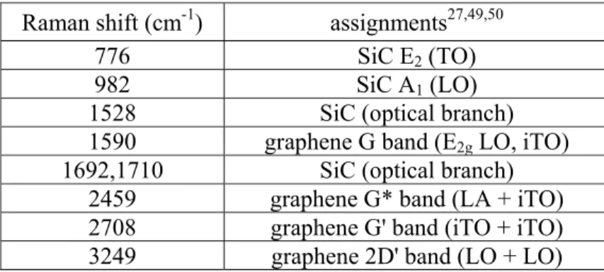
TERS spectra of epitaxial graphene
Tip-attached, tip-retracted, and subtracted (TERS) spectra of single-layer epitaxial graphene on the C-face of SiC are shown in Figure 1. Band assignments are summarized in Table 1. One of the two most prominent peaks, the G band, is the only band of graphene that originates from normal first-order Raman scattering. This band arises from a doubly degenerate in-plane transverse optical phonon (iTO phonon) and a longitudinal phonon (LO phonon) around the Γ point in the first Brillouin zone. Another intense peak, the G' band (also called the 2D band), is contributed by a double resonance process of two iTO phonons around the K point.27 The spectra in Figure 1 give typical features of single layer graphene such as a high intensity ratio between the G'/G bands (> 1) and a small FWHM of the G' band (~23 cm
-1). Note that not every area in this sample provides the spectrum of single layer graphene,
which is correlated with a sample average of 1.7 layers measured using visible light absorption. The D band (~1350 cm-1), which emerges from the double resonance process of
defects and iTO phonons around the K point,27 is absent in the spectra, indicating high quality graphene sheet with minimal defects. By considering the ratio of probe areas between TERS and far-field Raman spectroscopy (1:180), the enhancement factor in Figure 1 can be evaluated to be ~55 for graphene G' band and ~32 for SiC E2 band. Nevertheless, the
enhancement factor is greatly dependent on the tip quality. We recently reported an enhancement factor up to 1000 using the same instrument and a similar sample.48 The larger enhancement in graphene bands compared to SiC bands is due to the influence of the carbon buffer layer on the C-face (0001 face) of SiC. The effect of buffer layer on the difference in enhancement factor was discussed in our previous paper.48
Table 1. Band assignments for the spectra in Figure 1.
Raman shift (cm-1) assignments27,49,50 776 SiC E2(TO)
982 SiC A1 (LO)
1528 SiC (optical branch) 1590 graphene G band (E2g LO, iTO)
1692,1710 SiC (optical branch) 2459 graphene G* band (LA + iTO) 2708 graphene G' band (iTO + iTO) 3249 graphene 2D' band (LO + LO)
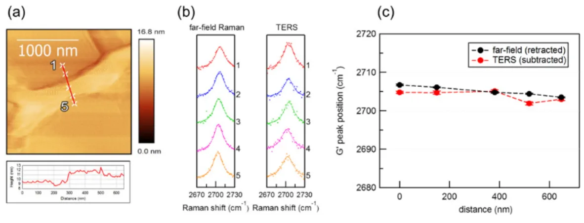
TERS spectra of step and ridge nanostructures
The epitaxial graphene forms patch-like areas throughout the sample. Data from AFM topology suggests that most areas are very flat (a few nanometers in height variation). However, in some areas, the epitaxial graphene shows unusual features that are not found in graphene from mechanical cleavage; for example, a step nanostructure is shown in Figure 2a. This step is about 2 nm high and originates from the step-terrace structure initially present on the SiC substrate. Figure 2b shows the G' band region of far-field Raman (tip retracted) and TERS (tip attached minus tip retracted) spectra obtained from five points across the step shown in Figure 2a. They all provide high IG/IG' ratios (> 1) and small FWHM of G' band (18
25
– 23 cm-1), which are characteristics of single-layer graphene. Although twisted double-layer graphene with G and G' bands similar to single layer graphene is commonly seen on epitaxial graphene,51 our Raman spectra do not show the characteristic I band (~1375 cm-1) of twisted
double layers.28 This confirms that the step structure does not arise from a difference in the
number of graphene layers, but rather from the inherent structure of the substrate. This structure, however, does not affect the G' band position significantly in both far-field Raman and TERS spectra (Figure 2c). The absence of a phonon frequency change implies that there is no significant strain difference between graphene on either side of the step.
A different nanostructure, on the contrary, alters the strain and causes the position of the G' band to change. Figure 3a depicts an AFM image of a ridge nanostructure. This ridge is the result of a difference in thermal expansion coefficients between graphene (measured: -1 × 10⁻⁶ K-1 @ 300 K, calculated: negative throughout 0–2000 K) and the SiC substrate (4.5 × 10
-6 K-1).52,53 Upon cooling from the synthesizing temperature, SiC shrank faster than graphene.
Thus, the graphene sheet experienced compression. When the compressive strain is greater than critical buckling strain, some parts of the graphene sheet are pushed out of the plane to form a ridge.54 This compression-induced ridge-forming mechanism is well-explained in
many papers.11,12,14,15 The AFM topology image in Figure 3a shows the ridge to have a ~6 nm
height and a ~ 150 nm width. Far-field Raman and TERS spectra shown in Figure 3b were obtained from seven points across the ridge. Since the points are not exactly on a straight line, the distances shown in Figure 3c, 3d, and 3e were measured using the point on the line nearest to each measurement point. Every TERS and far-field Raman spectrum in this area exhibits the G' band FWHM and IG/IG' ratio of single-layer graphene. For the points on the ridge, the
graphene G' bands in the TERS spectra (Figure 3b) have lower Raman shifts compared to bands in far-field spectra. The plot of peak position from Lorentzian fitting in Figure 3c clearly demonstrates the capability of improved spatial resolution with TERS. In TERS spectra, the G' band shows a Raman shift reduced by 8.7 cm-1 on the ridge compared to the flat area. Since the tip was controlled by non-contact mode AFM, the spectral change is
certainly not from a deformation caused by the tip. Therefore, the lower Raman shifts must come from the nanostructure. In the far-field Raman spectra, the peak shift caused by the ridge is very small because the spatial resolution of far-field Raman is larger than the nanoridge, and thus the signal from the ridge is obscured by the signal from the large neighboring flat area. Our Raman microscope has a spatial resolution of 1 µm, while the spatial resolution of TERS is in the same magnitude with the tip radius.36,37 (The tip used in this experiment had a tip radius of 75 nm.)
Generally, the shift of the G' band to a lower wavenumber is associated with a phonon softening process induced by bond lengthening from tensile (stretching) strain.25,55 Nevertheless, if we compare the G' band positions of our study to the 2674 cm-1 of free-standing graphene with no external strain (Beriaud et al., measured with the same excitation wavelength as in our experiment),56 the G' band on the ridge (2691 cm-1) is closer to free-standing graphene than the G' band of nearby flat areas (2700 cm-1). Therefore, the band downshift observed on this nanostructure is the result of reduced compressive strain relative to the nearby area, rather than tensile strain. The strain presents on the ridge and flat area can be calculated by the relationship:24
∆ ∆ 1
where , , ∆ , and ∆ are the observed G' band position, unstrained and undoped G' band position, position shift cause by mechanical stain, and shift cause by carrier doping, respectively. The mechanical part then can be calculated by:23
27
for uniaxial strain, where is the Grüneisen parameter for the G' band, is Poisson’s ratio for graphene or substrate and is the strain of the graphene sheet. For biaxial strain, which assumes equivalent strain on both axes, the equation is:
∆ 2 3
Although the carrier doping term is difficult to evaluate, by assuming negligible doping difference between graphene on the ridge and the surrounding area, the doping term can be eliminated in the calculation of the strain difference between two measurement points.
Relative strain on each point across the ridge in Figure 3d and 3e is calculated using 2674 from unstrained suspended graphene56, a Grüneisen parameter
2.7 for uniaxial strain23,25, 2.8 for biaxial strain24, Poisson’s ratio 0.231 for
SiC57 due to the attraction of graphene to the substrate25, and the TERS spectra on point 1 (flat area) as a reference. It is worth noting that many references report differing Grüneisen parameter values for G' band and Poisson’s ratio values for graphene/SiC.23–25,55,57–59 The
details of the calculation, including calculated strain using different constant values, are available in the supporting information.
With the results from the TERS spectra, the maximum strain difference is found on point 5 (ridge) with uniaxial strain of (1.6 ± 0.2) × 10-3 and biaxial strain of (5.8 ± 0.6) × 10-4. The positive values denote smaller compressive strain on the ridge (since compressive strain is assigned with negative value, a positive difference implies reduced compressive strain). This is an evidence for the proposed mechanism of Prakash et al.12 and Sun et al.11 that nanoridges of SiC-grown graphene form as a relief from the strain in epitaxial graphene grown on SiC. This is also the first time that strain on a nanoridge of epitaxial graphene was measured using TERS. Our calculated strain value for each point falls between the empirical minimum of 1 × 10⁻³ and the theoretical maximum of 8 × 10⁻³ reported by Ferralis et al.26