Study on the formation behavior of FeN
nano-structure on surface
of Si(111)-7×7-CH
3
OH
Si(111)-7×7-CH
3
OH 表面における
FeN ナノ構造の形成過程に関する研究
Wenxin Li
Table of Contents
Chapter 1 Introduction...1
1.1 Development of atomic level technologies and smart materials industry...1
1.2 Purpose of this research...13
Reference...16
Chapter 2 Mechanism of alcohols on a Si(111)-7×7 surface studied by scanning tunneling microscopy... 21
2.1 Introduction of the reconstructed Si(111)-7×7 surface...21
2.1.1 Introduction of the DAS model... 21
2.1.2 Preparation of reconstructed Si(111)-7×7 surface...23
2.1.3 Ladder region of Si(111) substrate... 25
2.2 Adsorption process analysis of the alcohols gas...27
2.2.1 Preparation of vacuum environment... 27
2.2.2 Investigation on the experimental system in STM...28
2.2.3 Analysis of atoms distribution based on LEED...30
2.3 Comparison of adsorption process of methanol, ethanol and propanol... 34
2.3.1 Detect the dissociation process by mass spectrometer...34
2.3.2 Study on the Adsorption mechanism of Alcohol...37
2.3.3 Comparison the adsorption condition of different situation on Si(111)-7×7-alcohol surface... 39
2.4 Classification of different metal clusters on silicon surface...41
2.5 Explore the dual characteristics of CH3OH to the metallic atomic structures43 2.5.1 The vertical (isolation) characteristic of methanol...43
2.5.2 Evaluation on distribution behaviors after heating by current... 47
2.5.3 Explore the new rulers of metal-H+models... 48
Concluding remarks...52
Reference...53
Chapter 3 Growth of Fe clusters on the Si(111)-7×7 surface saturated with CH3OH..57
3.2 The realization of the steaming process of the Fe atoms...58
3.2.1 Atomic layer deposition...58
3.2.2 Realization of metal atom steaming process... 60
3.2.3 Investigation on scanning mode for metal deposition...61
3.3 The original discovery of linear Fe clusters structure on Si(111)-7×7...63
3.4 Improvement of structural properties in iron cluster...64
3.4.1 Investigation on cluster property of metal dot...64
3.4.2 Observation on the effect of position adjustment of methanol adsorption..66
3.4.3 The relationship of steaming temperature and crystal structure...68
3.5 The proposal of a double layers iron cluster model... 69
3.6 Study on linearity of ultrathin films... 72
3.6.1 Concept of Stacking model... 72
3.6.2 Explore linear Fe clusters on Si(111)... 73
3.7 Stability verification for large-scale application... 74
3.7.1 The investigation and comparison of structure dimensions... 74
3.7.2 Analysis of element distribution based on XPS... 77
3.7.3 Results of STM-XPS in thin-air condition...79
Concluding remarks...82
Reference...83
Chapter 4 Formation process and mechanism of iron-nitride compounds on Si(111)-7×7-CH3OH surface... 87
4.1 Introduction... 87
4.2 Atomic-level material and its catalytic theory...88
4.2.1 The theory of quasi-compound...88
4.2.2 The theory of transformation state... 90
4.3. Structural analysis of iron-nitride...92
4.3.1 High resolution observation at high concentration...92
4.3.2 High resolution observation at low concentration...94
4.4 Introduction of magnetic measurement...98
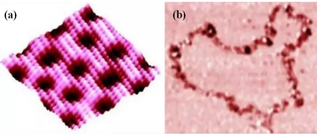
4.5 The original discovery of linear FeN clusters structure on Si(111)-7×7... 101
4.5.1 Experiment on the adsorption of NH3... 101
4.5.2 The evaluation of magnetic intensity... 103
4.5.3 The comparison experiment on the N+ion bombardment...105
4.6 Thickness-dependent mechanism and magnetic properties of iron-nitride..107
4.6.1 Improvement of steaming technology on thickness... 107
4.6.2 Thinner outcome of iron-nitride... 108
4.6.3 Improvement of dissociation efficiency... 110
4.7 Analysis of the relationship between magnetism and structure...113
4.7.1 Investigation on magnetism of nanoclusters... 113
4.7.2 Study on the formation of magnetic units... 114
4.7.3 Analysis of magnetic results...116
4.8 Stability verification for large-scale application...119
Reference...122
Chapter 5 Conclusions and recommendation 5.1 Conclusions... 125
5.2 Recommendation...128
Related publications... 129
Abstract
In recent years, metal clusters and metallic compounds grow on the surface of silicon which are promising for low cost high density devices. In this study, Fe atoms were deposited on the Si(111)-7×7 surface, which has been saturated with the CH3OH
Chapter 1 Introduction
1.1 Development of atomic level technologies and smart
materials industry
In the process of human social development, the level of material development has always been a sign of age and social civilization. With the rapid development of the smart materials industry, the size of electronic components and devices becomes smaller and smaller [1,2]. Accordingly, thin film materials are given high expectations, such as the regular structure of metal clusters and the high-density of memory units [3-5]. In recent years, atomic level technologies have increased the interest of researchers [6]. The 2016 Nobel Prize in chemistry was awarded to Jean-Pierre Sauvage, J. Fraser Stoddart and Bernard L. Feringa for "inventing molecular machines that can move in a controlled manner and perform tasks when given energy" [7]. The development of atomic level technology has led to the miniaturization of the technological revolution. That year's Nobel Prize in chemistry has brought Physical/Chemistry research into a new field. Using energy to control the movement of molecules, atomic technology has made scientific research out of the stalemate. From a developmental point of view, molecular machines for us are like motors for people in the nineteenth century. They didn't know that these coils and magnets would become trams, washing machines, fans and so on. Molecular machines can be useful in future new materials, sensors and energy storage systems.
into business applications. For example, the Nissan scratch-proof iPhone case [10], introduced in 2012, is based on work of professor Ito Kozo in the university of Tokyo. The material it used is made from a polymer chain that passes through a number of the rings, forming an "eight" shape. When a common polymer coating is subjected to pressure, the connections between the polymer chains are broken, resulting in scratches. But in this material, the cyclodextrins allow the polymer chain to slide smoothly under stress without damage. A film made of this material can even keep the phone's screen from breaking under the hammer. All of these cases mean that the molecular parts of atomic technology are mature enough to apply. Since the research of this field has experienced a long way, now it is the time to prove that they are useful to the world.
Table. 1.1 Comparison of several detection equipments and their functions Equip
ment Resolution environmentWorking temperatureOperating damageSample Detectingdepth
STM Atoms can be observed directly. Horizontal resolution: 0.1 nm Vertical resolution: 0.01 nm Atmosphere, solution, vacuum Low temperature, room temperature, high temperature None atomic1-2 layer TEM Horizontal resolution: 0.3-0.5 nm Horizontal lattice resolution: 0.1 nm -0.2 nm Vertical resolution: none High vacuum Low temperature, room temperature, high temperature Medium Equal to sample thickness (<100 nm) SEM Using secondary electron imaging. Horizontal resolution: 1-3 nm Vertical resolution: low High vacuum Low temperature, room temperature, high temperature Slight 1 μm FIM Horizontal resolution: 0.2 nm Vertical resolution: low Ultra high
vacuum 30-80 K Serious thicknessAtomic
Fig. 1.1 The basic structure diagram of STM
Compared with the analysis technology such as TEM, SEM [16, 17], scanning tunneling microscopy (STM) has the following features:
(1) The system of STM has a simple structure.
This wide range is any other kinds of microscopy techniques unable to achieve at present.
(4) High resolution. The scanning tunneling microscope has horizontal/vertical resolution of 0.1 nm and 0.01 nm, respectively. Therefore, individual atoms on the surface of the material can be directly observed, as well as their three-dimensional image.
(5) In the observation process of material surface structure, the sample can also be studied with scanning tunneling spectroscopy (STS). So that, chemical structure and electronic state of the material surface can be known.
(6) Unable to detect deep information and can not observe insulators directly.
A sharp metal probe is used to scan the sample surface. By using the quantum tunneling effect of the nanometer gap between the tip and sample, the tunnel current and the gap size show an exponential relationship, and the surface topography features of atomic samples are obtained. Scanning tunneling microscopy (STM) can be used to directly observe whether the surface atoms of materials have periodic surface structural characteristics, surface reconstruction and structural defects (Fig. 1.2).
The future development of this field should start from two aspects: At the micro level, these molecular machines can complete the tasks that cannot be completed by other means; At the macro level, trillions of atomic-scale components are used to reshape material properties. For example, some components are made to raise something much heavier than themselves, like ants. So that, when the concentration of metal atomic adsorption was low, researchers usually explored the single atom mechanism on the substrate (Fig. 1.3) [18, 19]. By contrast, the application of thin film adsorption was studied at higher concentration [20]. Since the specific cluster models were not clear, the formation process between the two subjects could not be accurately controlled [21]. In recent years, researches around the different compounds or clusters have increased the interest of researchers [22].
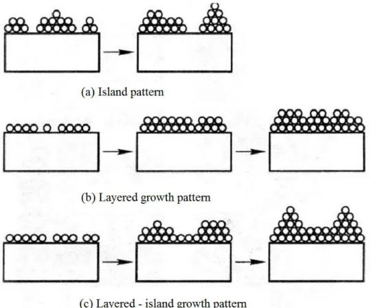
Fig. 1.4 Three different film growth patterns
Unlike the bulk material, thin film material is a layer of material deposited or prepared on the surface by special methods, as shown in Fig. 1.4. Thin film materials are valued because it usually has special performance or combination performance [23, 24]. The key part of film science is the study of the growth process of film, which can be divided into three patterns [25, 26].
(1) Island pattern
At the initial stage of film formation, the core is formed according to the three-dimensional nucleation mode, and the stable core grows into isolated islands. The islands are then merged into continuous films, such as Au films on SiO2substrate.
In this growth mode, atoms or molecules of sediment tend to bond with each other rather than with substrate atoms. That is, the wettability between the deposited material and the substrate is weak.
When the wettability between the deposition and the substrate is good, the atoms tend to bond with the substrate atoms. From the initial stage of film formation, the films have been grown in a two-dimensional expansion mode, such as Si films on Si substrates. In this mode, there is no significant stage of nucleation. Each layer is automatically spread on the surface of the substrate or film to reduce the total energy of the system.
(3) Layered - island growth pattern
In the initial stage of film formation, several layers were formed according to the two-dimensional layered growth. After that, the growth mode was transformed into island mode, such as Ag films on Si substrates. The physical mechanism leading to this mode transition is quite complex, and the fundamental reason can be attributed to the growth and decline of various energy in the process of film growth. For example, due to the mismatch of lattice constants between thin films and substrates, in order to reduce strain energy, island mode is transformed into island mode, and so on.
World's new material industry is at a stage of development from low level to high level, with a wide range of application scope [27-29]. In the process of communication and cooperation, smart materials industry presents a rapid development trend, especially in some key areas. Significant results have been achieved in development potential, environmental protection and resource utilization. With the rapid development of the world's social economy, emerging industries have been constantly optimized and upgraded. As a result, the demand for new smart materials is constantly expanding in all markets. At present, new materials have accounted for 15-20% of the output value of high-tech industries in developed countries. Its research/development capacity and industrialization scale have evolved into the important measurement of one country's overall economic and social development as well as national defense strength. However, there are still serious problems in the innovation process of new materials.
(1) Definition of smart material industry
As the smart material industry was initially formed in the middle and late last century and newly developed in the beginning of this century, there is no clear and stable concept definition of new material industry. However, there should be a relatively unified and rigorous logical starting point for research. In this paper, intelligent material was divided into two categories:
(Ⅰ) Embedded smart materials, also known as smart material structure or intelligent material system. On the substrate material, three types of materials are embedded, including sensor, motion and control functions. Sensor components collect and detect the information given by the external environment. The control processor is responsible for directing and motivating the motion components, so the corresponding actions are executed.
(Ⅱ) The micro-structure itself has intelligent features. The performance can be carried out with changes in environment, time and so on. For example, a smart gel based on light/chemical signals may be used to produce an adjustable lens or sensor. Some similar products are also popular, such as filters, InP semiconductors, etc.
(2) Comparison between materials and smart materials
It is particularly important to note the differences between materials and new materials. Materials are substances that can be directly used to make objects, components or devices [32]. Compared with traditional materials, new materials industry is characterized by high technology density, high investment in research and development, high added value of products, strong international production and market, wide application range and good development prospect. etc. Smart materials industry, including new materials and related technical products/equipments. Specifically, it mainly includes three aspects: (Ⅰ) the industry formed by new materials itself; (Ⅱ) the manufacturing of new materials technology and equipment; (Ⅲ) the improvement of traditional materials technology Industry, etc.
(3) Nano-material technology and its innovation process
begun to enter the stage of industrialization, especially in the transformation of traditional and nano-composite materials. At the same time, the transformation of nano-material technology from manufacturing to industrialization has been realized step by step. The innovation process of nano-material industry and even the whole smart material industry is different from that of general industry. It is not only a progressive innovation in a certain field, but also a process of bringing new changes to multiple applications. With the development of technology, nanotechnology has gradually stepped down from the altar of gods. From the initial advanced industry, nanomaterial gradually expands to the field of cosmetics, textiles and the like, which is more closely related to the life of people.
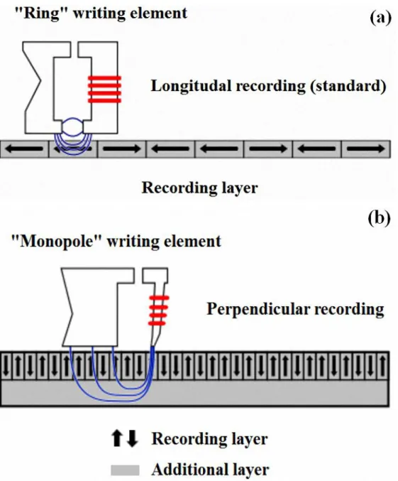
Fig. 1.5 Structure diagrams of (a) longitudal recording and (b) perpendicular recording.
decreasing their size [45-47]. Accordingly, the preparation of single magnetic domain clusters is an interesting challenge to magnet materials for high-density magnetic recording medium. So far, the reported critical sizes for single magnetic domains were 85 nm for Ni, 40 nm for Fe3O4, and 16 nm for α-Fe [45-47], and the cluster with a size
lower than the critical value displays super paramagnetism, which could not be applied for the magnetic recording medium. To improve the density of magnetic recording without the restriction of super paramagnetism, it is necessary to prepare the single magnetic domain clusters with limited critical size. Human research on iron nitride material has a long history, which was first discovered in the hardened layer of nitriding treatment on steel surface. The systematic study of gasified iron began in 1928, when the structure of iron-nitride was studied by X-ray diffraction. Subsequently, the magnetism of iron-nitride was experimentally studied in 1930. Finally, in 1946, γ'-Fe4N was found to have a large saturation magnetic moment after.
The series of iron-nitride compounds began to attract widespread attention. From this view point, FeN single magnetic domain clusters have become the research focus, which could be analyzed for the spin in physics, ontrollable surface reaction in chemistry, for example, FeN and FeOx with the critical size lower than 10 nm.
1.2 Purpose of this research
Nano-magnetic materials are one of the most important research fields in the world. At present, there are many kinds of nano-magnetic materials, such as ferrite, γ-Fe2O3, Fe3O4, BaFe12O9, metal magnetic powder, rare earth alloy and iron-nitride
regular structure is desired not only for the fundamental studies, but also for the application of high-density magnetic memory thin film. The Fe clusters were prepared by many techniques [48-51]. Magnetic units are adsorbed on the surface of substrate, forming a stable arrangement. Taking advantage of strong magnetism, the atomic structure of Fe was considered in this study. In order to improve the density of magnetic storage unit, the iron cluster are formed as well as their multi-layer model. However, since the magnetic property of existing Fe compounds is weak, this study tried to nitride it with adsorption gas. Concerning the stability of the iron compound in the nitrogen and oxygen environment, this paper tends to focus on NH3 gas. Using
mass spectrometer and gas adsorption device, the previous hypothesis is confirmed. Methanol and ammonia have similar adsorption mechanism, and the specific process can be defined. As discussed in a previous breaking gas, the ammonia synthesis reaction on Fe catalysts is catalyzed by a cyclic process consisting of the formation of the quasi-compound FexNHyand its rapid change to FexN. When the concentration is
relatively high, although FexN compounds continue to grow steadily on the surface of Si(111)-7×7-CH3OH, the linearity of them is quite confusing. By adjusting the
concentration of ammonia, the preliminary formation stage of iron-nitride compounds has been figured out. In particular, some specific classifications, including the concept of precursor compounds could to be verified and summarized. Different formation mechanism corresponds to different cluster shapes, the most suitable growth pattern could be found with the 3D images of STM. As a result, the thickness of iron clusters was confirmed to be the key to the dissociation process. With the introduction of Ar, the adverse influence of metal deposition was solved effectively. As a result, 2 typical Fe3Nxmodels have promoted the formation rate of the stable structure greatly. Finally,
Reference
1 Seminario, J.M. Molecular Electronics Approaching Reality. Nat. Mater. 2005, 4, 111–113.
2 Quapp, W. A minimal 2D model of the free energy surface for a unidirectional natural molecular motor. J. Math. Chem. 2018, 56, 1339–1347.
3 Alam, K.; Disseler, S.M.; Ratcliff, W.D.; Borchers, J.A.; Ponce-Pérez, R.; Cocoletzi, G.H.; Smith, A.R. Structural and magnetic phase transitions in chromium nitride thin films grown by RF nitrogen plasma molecular beam epitaxy. Phys. Rev. B 2017, 96, 104433.
4 Zygmanski, P.; Sajo, E. A self-powered thin film radiation detector using intrinsic high energy current. Med. Phys. 2016, 43, 4–15.
5 Bartolomé, J.; Bartolomé, F.; Brookes, N.B.; Sedona, F.; Basagni, A.; Forrer, D. Reversible Fe magnetic moment switching in catalytic oxygen reduction reaction of Fe-phthalocyanine adsorbed on Ag(110). J. Phys. Chem. C 2015, 119, 12488–12495.
6.Warner, B.; Gill, T.G.; Caciuc, V.; Atodiresei, N.; Fleurence, A.; Yoshida, Y.; Hirjibehedin, C.F. Guided Molecular Assembly on a Locally Reactive 2D Material. Adv. Mater. 2017, 29, 1703929.
7 Sauvage, J. P., Stoddart, J. F., & Feringa, B. L. (2016). The noBel prize in chemisTry 2016. The UKRAINIAN, 138.
8 Walsh, C. (2000). Molecular mechanisms that confer antibacterial drug resistance. Nature, 406(6797), 775.
9 Tour, J. M. (2000). Molecular electronics. Synthesis and testing of components. Accounts of Chemical Research, 33(11), 791-804.
10 Ball, P. (2015). Material witness: Concrete mixing for gorillas. Nature materials, 14(5), 472.
11 Y. Sugimoto, Y. Nakajima, D. Sawada, et al., Simultaneous AFM and STM measurements on the Si (111)−(7×7) surface, Phys. Rev. B 81 (2010): 245-322.
microscopy measurements on InAs/GaSb nanowire Esaki diode devices, NANO. RES. 7.6 (2014): 877-887.
13 Hansma, P. K., Elings, V. B., Marti, O., & Bracker, C. E. (1988). Scanning tunneling microscopy and atomic force microscopy: application to biology and technology. Science, 242(4876), 209-216.
14 Tseng, A. A., Notargiacomo, A., & Chen, T. P. (2005). Nanofabrication by scanning probe microscope lithography: A review. Journal of Vacuum Science & Technology B: Microelectronics and Nanometer Structures Processing, Measurement, and Phenomena, 23(3), 877-894.
15 Magonov, S. N., & Whangbo, M. H. (2008). Surface analysis with STM and AFM: experimental and theoretical aspects of image analysis. John Wiley & Sons.
16 Grabulov, A., Ziese, U., & Zandbergen, H. W. (2007). TEM/SEM investigation of microstructural changes within the white etching area under rolling contact fatigue and 3-D crack reconstruction by focused ion beam. Scripta Materialia, 57(7), 635-638.
17 Stevie, F. A., Vartuli, C. B., Giannuzzi, L. A., Shofner, T. L., Brown, S. R., Rossie, B., ... & Purcell, B. M. (2001). Application of focused ion beam lift‐out specimen preparation to TEM, SEM, STEM, AES and SIMS analysis. Surface and Interface Analysis: An International Journal devoted to the development and application of techniques for the analysis of surfaces, interfaces and thin films, 31(5), 345-351.
18 T. Hashizume, K. Motai, Y. Hasegawa, et al., Alkali metal adsorption on the Si (111) 7×7 surface, J. VAC. SCI. TECHNOL. B 9.2 (1991): 745-747.
19 Q. Liu, Q. Fu, X. Shao, et al., Diffusion of single Au, Ag and Cu atoms inside Si (111)-(7×7) half unit cells: A comparative study, APPL. SURF. SCI. 401 (2017): 225-231.
20 Z. Zhang, M. G. Lagally, Atomistic processes in the early stages of thin-film growth, SCIENCE 276.5311 (1997): 377-383.
22 S. V. Sitnikov, A. V. Latyshev, S. S. Kosolobov, Advacancy-mediated atomic steps kinetics and two-dimensional negative island nucleation on ultra-flat Si (111) surface, J. CRYST. GROWTH. 457 (2017): 196-201.
23 Freund, L. B., & Suresh, S. (2004). Thin film materials: stress, defect formation and surface evolution. Cambridge University Press.
24 Eason, R. (2007). Pulsed laser deposition of thin films: applications-led growth of functional materials. John Wiley & Sons.
25 Ohring, M. (2001). Materials science of thin films. Elsevier.
26 Thompson, C. V. (1990). Grain growth in thin films. Annual review of materials science, 20(1), 245-268.
27 Smith, R. C. (2005). Smart material systems: model development (Vol. 32). Siam.
28 Leo, D. J. (2007). Engineering analysis of smart material systems. John Wiley & Sons.
29 Shrouf, F., Ordieres, J., & Miragliotta, G. (2014, December). Smart factories in Industry 4.0: A review of the concept and of energy management approached in production based on the Internet of Things paradigm. In Industrial Engineering and Engineering Management (IEEM), 2014 IEEE International Conference on (pp. 697-701). IEEE.
30 Klabunde, K. J., & Richards, R. M. (Eds.). (2009). Nanoscale materials in chemistry. John Wiley & Sons.
31 Silberglitt, R., Antón, P. S., Howell, D. R., & Wong, A. (2006). The global technology revolution 2020, executive summary: Bio/nano/materials/information trends, drivers, barriers, and social implications. Rand Corporation.
32 Akhras, G. (2000). Smart materials and smart systems for the future. Canadian Military Journal, 1(3), 25-31.
33 Thompson, D. A., & Best, J. S. (2000). The future of magnetic data storage technology. IBM Journal of Research and Development, 44(3), 311.
Physics Letters, 74(17), 2516-2518.
35 Sagawa, M., Fujimura, S., Togawa, N., Yamamoto, H., & Matsuura, Y. (1984). New material for permanent magnets on a base of Nd and Fe. Journal of Applied Physics, 55(6), 2083-2087.
36 Friedrich, H., & Schumann, S. (2001). Research for a “new age of magnesium” in the automotive industry. Journal of Materials Processing Technology, 117(3), 276-281.
37 Weiss P: Hypothesis of the molecular field and ferromagnetic properties.J Phys 1907, 4:661.
38 Landau LD, Lifshitz E: On the theory of the dispersion of magnetic permeability in ferromagnetic bodies. Phys Z Sovietunion 1935, 8:153.
39 Wood, R. (2009). Future hard disk drive systems. Journal of magnetism and magnetic materials, 321(6), 555-561.
40 Piramanayagam, S. N. (2007). Perpendicular recording media for hard disk drives. Journal of Applied Physics, 102(1), 2.
41 Grochowski, E., & Halem, R. D. (2003). Technological impact of magnetic hard disk drives on storage systems. IBM Systems Journal, 42(2), 338-346.
42 Wang, S. X., & Taratorin, A. M. (1999). Magnetic Information Storage Technology: A Volume in the Electromagnetism Series. Elsevier.
43 Werthamer, N. R. (1963). Theory of the superconducting transition temperature and energy gap function of superposed metal films. Physical Review, 132(6), 2440.
44 Neugebauer, C. A., & Webb, M. B. (1962). Electrical conduction mechanism in ultrathin, evaporated metal films. Journal of Applied Physics, 33(1), 74-82.
45 Mills DL, Bland JAC: Nanomagnetism: Ultrathin Films, Multilayers and Nanostructures. Amsterdam: Elsevier BV; 2006.
46 Cullity BD, Graham CD: Introduction to Magnetic Materials. Hoboken: Wiley;2009.
48 Ruder WC, Hsu CPD, Edelman BD Jr, Schwartz R, LeDuc PR: Biological colloid engineering: self-assembly of dipolar ferromagnetic chains in a functionalized biogenic ferrofluid. Appl Phys Lett 2012, 101:063701.
49 Ching WY, Xu YN, Rulis P: Structure and properties of spinel and comparison to zinc blende FeN. Appl Phys Lett 2002, 80:2904.
50 Šljivančanin Ž, Pasquarello A: Supported Fe nanoclusters: evolution of magnetic properties with cluster size. Phys Rev Lett 2003, 90:247202.
Chapter 2 Mechanism of alcohols on a Si(111)-7×7 surface
studied by scanning tunneling microscopy
2.1 Introduction of the reconstructed Si(111)-7×7 surface
2.1.1 Introduction of the DAS model
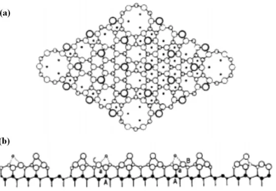
Silicon is an important semiconductor material, and the study on Si surface is always one of the main directions of the surface physical [1, 2]. As we know that the atoms can rearrange on the semiconductor clean surface or adsorption atom layer, in order to reduce the surface energy, which is called the “surface reconstruction”. According to different treatment conditions, Si surface reconstruction varies, such as 1×1, 2×1, 2×2, c2×4, c2×8, √3×√3, n×n (n is odd, n>1) [3-6]. However, 7×7 surface reconstruction is one of the most complex surface reconstruction in Si(111). It was studied almost at the same time as the emergence of surface science. For the unreconstructed Si(111) surface, there should be 49 suspension keys in the 7×7 surface. It's a very high-energy surface, very unstable. The atoms will be rearranged and reconstructed into a stable 7×7 structure under certain conditions. Each reconstructed 7×7 cell contains only 19 dangling bonds, distributed over 12 top atoms, 6 stationary atoms and 1 hole atom. The tunneling current in STM scanning process basically comes from these suspension keys.
subunits, and two dips on each side of the triangular subunits. The model structure contains 19 dangling bonds (18 dangling bonds for the adatoms and for atoms in the top layer which are not bonded to the adatoms and one dangling bond for the atom below the vacancy at the corner). The number of the dangling bond is the lowest for the present model among the proposed models. The energy barrier of the diffusion from unfaulted-HUC (UHUC) to faulted-HUC (FHUC) along this pathway is 0.79 eV. In the middle of each of these two pathways, there is a metastable adsorption site rendering the diffusion to be a two-step process. The energy barriers of the rate determining processes in UHUC to FHUC diffusion (forward diffusion) and the reverse diffusion (backward diffusion) along these two pathways are about 1 eV.
2.1.2 Preparation of reconstructed Si(111)-7×7 surface
The Si single crystal was cut along the direction perpendicular to [111], that is, the 1×1 structure of the (111) surface was obtained. Each of its surface atoms has a dangling bond, so the surface energy of this structure is very high and very unstable. Once exposed to the atmosphere, a thicker oxide layer will form on the surface. In order to obtain a clean Si(111) surface, the vacuum of the preparation chamber is better than 10-7 Pa. Si(111)-7×7 reconstruction is the most stable of all surface
structures [7, 8], which can be formed using a flash heating [9-11]. The sample is heated to about 600 °C and kept at this temperature for 12 hours, so that the sample can be fully degassed. Then, the sample is rapidly heated to about 1200 °C to remove the oxide layer as well as impurities on the surface. In this process, when the vacuum is reduced to 10-8Pa, the DC current should be switched off quickly and repeatedly, so
that the vacuum will not be reduced to 10-7 Pa by heating. So that, the sample is
heated to 1200 °C by direct current, then the temperature is slowly lowered. Repeat this process for 3 to 4 times, 7×7 reconstruction can be obtained, which has good periodicity and stability. Therefore, this surface is suitable to be used as a substrate material for epitaxial growth, which has an important significance to the study on surface properties.
Si(111) surface is one of the most intriguing problems in surface science. In recent years, a great number of impressive experiments and theoretical discussion are involved in this reconstructed structure. About its basic unit cell with 49 atoms, there were still many difficulties to derive a structural model unambiguously even from an abundant set of experiments. For a long time, almost every new model would inevitably conflict with other models proposed before. More and more models seem to confuse the problem rather than clarify the issue. In order to make significant progress, some basically new approach is required. The recently atomic-level technique introduced by scanning tunneling microscopy is the key breakthrough. Taking account of the different vectors observed in STM images, possible structure model is obtained. For a single large cell superlattice structure, it can be considered as composed of several structural components. It is noted that a DAS model was developed, which is abbreviated for dimer-adsorbing atom-adatom-stacking fault model. Comply with LEED, RHEED, ICISS [12-14], this model well explains the results of other experiments before.
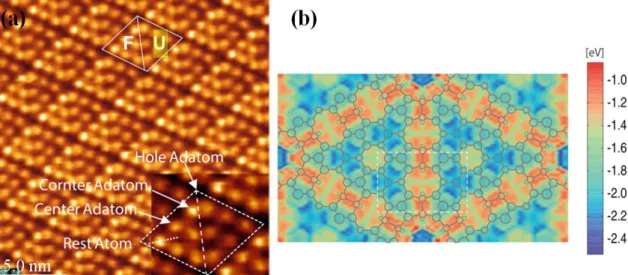
Fig. 2.2 (a) The STM image of Si(111)-7×7 reconstructed surface. Whether U structure or F structure, is composed of corner sites and center sites. (b) The calculated potential energy surface (PES) of an Ag adatom on the Si(111)-7×7 surface as well as the schematic top view of the surface structure.
2.1.3 Ladder region of Si(111) substrate
of the surface, but also play an important role in the surface electron density. The formation of ladder region is the result of gradual stretching of boundary areas. The degree of tension can be reflected by the height difference, just as shown in Fig. 2.3 When the height difference was relatively small, a cliff area could be found which regarded as the initial stage. With the expansion of the ladder region, a stable ladder region was formed (Fig. 2.3 (b)).
2.2 Adsorption process analysis of the alcohols gas
2.2.1 Preparation of vacuum environment
Surface analysis of low-dimensional nano-structure is a research process at nanoscale. Therefore, even small particles (such as atoms, molecules, ions, etc.) will have a serious impact on the results, which need the support of ultra-high vacuum technology. Generally, any state below atmospheric pressure can be called vacuum. The gas molecules distribution of vacuum is much rarer than that of ordinary state. So that, the collision frequency between molecules is greatly reduced. Vacuum technology is the basis of establishing vacuum environment. The research of this subject also depends on it to explore the characteristics on the substrate.
The equipment that can obtain and maintain vacuum state is called vacuum pump [23-25]. (1) The mechanical pump: Usually mechanical pumps, which are divided into oil seal type and dry type. We use the former one in our laboratory. (2) The turbomolecular pump: Since turbomolecular pumps can not work directly at atmospheric pressure, usually combined with a mechanical pump. We used one in the preparation chamber. (3) The sputtering ion pump: One ion pump is used in our observation chamber as the secondary pump. It works in 10-4~10-9 Pa environment,
which can maintain the ultra-high vacuum of the system. This pump is very effective in pumping away reactive gases (such as O2, N2, etc.). However, for inert gases (He,
Fig. 2.4 Physical and structural images of: (a) mechanical pump; (b) molecular pump; (c) ion pump; (d) vacuum gauge.
2.2.2 Investigation on the experimental system in STM
Our experiments were adsorbed and observed by JSPM-4500S ultra-high vacuum scanning tunneling microscopy (STM) system (JEOL Ltd., Akishima-shi, Japan). Experiments were performed in the observation chamber with a base pressure of 1×10− 8 Pa. And the vacuum degree is below the 4×10− 8 Pa in the preparation
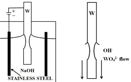
tips, such as shearing, electrochemical corrosion, etc [26, 27]. W tips are usually prepared by electrochemical etching. The schematic diagram of the device for preparing W tip by electrochemical etching is shown in Fig. 2.6. The dielectric solution we used is NaOH solution. Besides, it should be noted that tungsten is easy to oxidize in the atmosphere. The oxide layer is also formed on the surface. Therefore, special treatment must be carried out before we send it into the observation chamber.
Fig. 2.6 Schematic diagram of the electrochemical corrosion and the part of W probe.
The preparation chamber of the STM system is equipped with three sample holders, which can be used to make three specimens at the same time and conditions. The specific experimental procedures are as follows: Specimens were degassed in the preparation chamber at about 450 °C. Then, the sample was repeatedly flashed at 1250 °C until a clean well-ordered Si(111)-7×7 reconstructed surface was obtained. After cooling, the sample was transferred to the observation chamber. Through the needle valve, one set of gas storage device is connected with this chamber, which is full on different gas. During the adsorption process of alcohol, the mass spectrometer was turned on to monitor the gaseous molecules composition in the observation chamber.
2.2.3 Analysis of atoms distribution based on LEED
the diffracted electrons can be observed on the fluorescent screen. So, surface structures of the sample can be characterized. There are two important applications of low-energy electron diffraction:
(1) Qualitative analysis
Focusing on the analysis of diffraction pattern and spot location, the symmetry of surface structures can be obtained. If there are adsorbents on the surface, the unit lattice and relative size/direction of them can be determined by qualitative analysis.
(2) Quantitative analysis
It is mainly concerned with the relationship between the intensity of the diffracted electron beam and the energy of the incident electron beam. Further compare I-V curves with the theoretical prediction, the exact position information of surface atoms can be obtained.
The ultrahigh vacuum (UHV) system consists of a main chamber and a preparation chamber with a base pressure of 2×10⁻¹⁰Torr. The observation chamber is
equipped with a 4 grid-LEED/AES optics for sample surface characterization (model: BDL600IR) and a Gammadata Scienta SES-100 analyzer for sample surface composition. The preparation chamber is equipped with conventional UHV surface preparation and analysis tools. Si(111)-7×7 restructured surface and Si(111)-7×7-alcohol surface were be observed by LEED. In this process, the filament current was 2.8 A, the screen voltage was 4.0 kV, and the beam energy was 60 eV. The sample was moved into observation chamber for LEED measurement. Then the ethanol was introduced slowly into preparation chamber for 2 min at the pressure of 1×10⁻⁶Torr. The Si(111)-7×7-alcohol surface was observed again by LEED.
Fig. 2.8 LEED patterns of Si(111)-7×7-alcohol surface (from 110 eV to 180 eV)
2.3 Comparison of adsorption process of methanol, ethanol and
propanol
2.3.1 Detect the dissociation process by mass spectrometer
separated by charge to mass ratio. Mass spectrometry analysis is a kind of instrument for separating and detecting samples according to the principle that charged particles would deflect in the electromagnetic field. Ions of different masses have different offsets as they pass through the magnetic field. After that, they would focus on different locations, obtaining different mass spectra of isotopes. That is, the mass difference of matter atoms, molecules or molecular fragments. The mass spectrometer consists of ion source, mass analyzer and ion detector. Main experimental conditions of the instrument are designed in vacuum. To a large extent, the performance of ion source determines the ionization efficiency as well as its sensitivity. Among them, there are two main technical parameters. One is the range of mass-charge ratio (mass range) that can be measured, the other is the resolution. If the mass spectrometer can precisely distinguish between mass m and m+Δm, the resolution is defined as m/Δm. At present, the resolution of modern mass spectrometer ranges from 105 to 106, which can measure atomic mass accurately to 7 digits after decimal point. By dissociation, ions enter the ion detector in turn and ion signals can be amplifying collected. Through computer processing, the mass spectra can be draw. We find out the main ion peak (generally refers to the relative strength of the larger ion peak), and then to record the mass of these peaks (m/z) and their relative strength.
Three Si(111)-7×7 samples were successively sent into the observation chamber, which is filled with CH3OH, C2H5OH and C3H7OH gas respectively. The tungsten tip
was retracted away from the surface to reduce shadowing effect of the tip. At the same time, the mass spectrometer is turned on to monitor the gaseous ion composition in the observation chamber. The samples can be preheated by an external power source. Although much research has been devoted to pure Si surface, little attention paid to its intermediate layer [32, 33]. In the case of adsorption of CH3OH, C2H5OH and
C3H7OH, the precursor state is equally formed in the faulted and unfaulted halves at
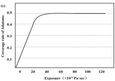
Alcohols’ adsorption on the Si(111)-7 × 7 surface was proved to have a constant sticking probability until saturation. In the same conditions, CH3OH is bound to have
higher reaction efficiency. When its adsorption time reaches about 30 s, the coverage rate can maintain the stable 49% (nearly 1/2). In the case of adsorption of alcohol, the precursor state is equally formed in the faulted and unfaulted halves at room temperature. By analyzing surface images, the ratio of occupied Si adatoms to unoccupied Si adatoms becomes finally 1:1 in the saturated adsorption of methanol. The adsorption of CH3OH, C2H5OH and C3H7OH on the Si(111)-7×7-alcohol surface
is a good example. If a clean Si(111)-7×7-alcohol surface is exposed to CH3OH or
C2H5OH (R-OH), the molecules dissociate into Si-OR and Si-H on a pair of (Si
adatom/Si rest atom) as described schematically in Fig. 2.9 (d).
Fig. 2.9 Mass spectra images of (a) CH3OH, (b) C2H5OH and (c) C3H7OH. (d) is
2.3.2 Study on the Adsorption mechanism of Alcohol
In Figure 2.10, according to the analytical method mentioned above, each triangle on Si(111)-7×7 surface is composed of six adsorption sites. In Figure 1 (a), according to the analytical method mentioned above, each triangle on Si(111)-7×7 surface is composed of six adsorption sites. Further, every six sites can also be divided into 3 center sites (red) and 3 corner sites (blue). Then, aim to analyze the specific dissociation process, based on the real-time monitoring data of mass spectrometer, the gas ion’s composition in the cavity is simultaneously known (Fig. 2.8). There is a dissociation process in the adsorption stage of each alcohol gas:
) ( 3 H + O H C = OH H C (2) H + O H C = OH H C (1) H + O CH = OH CH -7 3 7 3 + -5 2 5 2 + -3 3
The STM image of adatoms and the tunneling spectroscopy at the rest atom position suggests that the CH3OH molecule dissociates on an adatom and rest atom pair by
forming Si-OCH3and Si-H, respectively. These facts indicate that the dissociation of
the alcohols is accomplished via a precursor state in each half unit cell: that is, each half unit cell works independently as if it was a molecule. It is known that H2O, NH3
and CH4 undergo dissociation on a pair site of Si-adatom and Si-rest atom, where the
dangling bond on the Si-adatom is empty while that on the Si-rest atom is almost filled. Taking these facts into account, we infer that the key to the adsorption of alcohols is OH- rather than (CH+)n. Although there is no quantitative test, by
observing the relative intensity data of ions in the cavity, we can find: The chemical reaction efficiency of H+ and Si is much higher than that of C2H5O- or CH3O-. This
Then, we selected CH3OH for further study. Every triangular half unit cell
contains three Si-OCH3 and three Si ad-atoms, which the former show as the bright
dots and the latter is relatively dark in the STM image. The rest atoms on the lower layer of the substrate are further reduced at the height in the STM image and cannot be scanned. H atoms saturate the suspended key of rest atom, which also cannot be observed clearly. From the theoretical point of view, metal atom on the Si(111)-7×7 surface undergoes migration by hopping among Si-adatom and Si-rest atom. In this paper, we studied the deposition of metals on the Si(111)-7×7 surface saturated with CH3OH, on which the whole Si-rest atoms are changed to Si-H so that the hoping
migration of metal will be prohibited. More than this, CH3OH coating can also
effectively prevent the formation of FeSi, whose magnetic property is much lower than that of the pure Fe atom. In this paper, after understanding the specific adsorption mechanism of CH3OH, we will use it to improve the success rate of Fe atomic linear
Fig. 2.10 (a) STM image of the Si(111)-7×7 surface with CH3OH concentration
is 10-6Pa, and the gas adsorption time is 30 s; (b) The model of a half unit cell: three
pairs of Si-OCH3 and Si-H are formed at the adatom/rest sites; (c) Image of
relationship between methanol adsorption time and its coverage.
2.3.3 Comparison the adsorption condition of different situation
on Si(111)-7
×7-alcohol surface
As describe below, the alcohol molecule (ROH) does not directly dissociate by collision at a pair of Si adatom/Si rest atom, but undergoes dissociation via a transformation state on either a center-Si-adatom or a corner-Si-adatom site. As shown in Fig. 2.10, bright points corresponding to methanol ion. H atoms adsorb on rest Si atoms without moving, which are consecutively increased in each half unit cell. Therefore, saturated adsorption is attained when a half of the adatoms are changed to Si-OCH3 in every half unit cell. It is noted that the adsorption equally occurs on
faulted and unfaulted halves with a constant sticking probability until the surface is saturated as shown in Figs 2.11 (a) and (b). This important feature indicates that the sticking probability, process of transformation, is little influenced by preadsorbed Si-OCH3 and/or Si-H, although the dissociation probability (site selectivity) of the
obtained by the STM corresponds to the formation probability of the transformation state which goes to dissociation.
On the other hand, the STM image is formed in accordance with the site selectivity for the dissociation of the precursor. Therefore, the constant sticking probability does not mean the consecutive steps with an equal rate. As shown in Fig. 2.11 (b), the dissociation probability of a precursor state molecule is the same on the F-half compared to that on the U-half unit cell. It is worth noting that the adsorption (dissociation) probability of methanol (CH3OH) is exactly equal to that of other
alcohols (C2H5OH, C3H7OH) and their adsorption probability has a constant value up
to the saturation. Moreover, the distribution of methanol is found identical on both regions of flat and ladder (Figs. 2.11 (c) and (d)). On the ladder region, methanol is evenly distributed. Whether in the FHUC/UHUC triangle or corner/center, methanol has no obvious adsorption bias, maintaining the probability of 1:1. Continue to increase the concentration, methanol does not grow in layers, nor does it form cluster. These facts all indicated that CH3OH can be used as an ideal intermediate layer in the
Fig. 2.11 (a) Consecutive change of the fraction of half unit cells with one, two, and three adsorption sites as increasing exposure. (b) Coverage of U/F cells increased with the exposure of CH3OH. (c) and (d) are the origin/stable ladder region with
CH3OH concentration is 10-6Pa, 45 s.
2.4 Classification of different metal clusters on silicon surface
As the important substrate material, the reconstructed Si(111)-7×7 is a surface with well established atomic and electronic structures. Epitaxial growth of it attaches much significance to potential applications on diverse areas, like smart materials industry. The recent progress in the multi-layer adsorption and its characterization, has increased the interest of researchers. Since 2004, the dynamics of metal atoms began to be concerned about. For example, a honeycomb layer composed of Sn2/Zn3 atoms
and Fe), some specific classifications could be verified and proposed (Fig. 2.12). Weak-compound is not easy to form a cluster structure, while strong-compound tends to hip or move because of its dynamic. Iron is classified as a quasi-strong compound since it can form stable clusters, but reacts with the substrate. A newly formed surface is stabilized by different atoms/molecules, forming different types of compounds. Moreover, the formation of each compound is always accompanied by a different degree of destruction on the surface. The characteristics of each reaction may be reflected by such a compound structure as the precursor state. As a quantitative concept, destruction could and should also be adjusted. In this paper, the introduction of the intermediate layer which could regulate the metallic compounds becomes the focus of our attention.
Fig. 2.12 Three typical compound models: the yellow one represents a weak-compound, which is enough stable to fix on the silicon surface; the blue one represents a strong-compound, which is easy to move and form cluster structure; the green represents a type of quasi-strong compound, which can not only form clusters, but also easy to fix on the surface.
2.5 Explore the dual characteristics of CH
3OH to the metallic
atomic structures
2.5.1 The vertical (isolation) characteristic of methanol
Firstly, we were concerned with the Fe compound, which has a good prospect of application. However, it is very easy to react with Si, resulting in the low magnetic strength. As a progressive approach, in Fig. 4a: Fe atoms were steamed on Si (111)-7×7 reconstructed surface, which was saturated by CH3OH molecules. Assisted
by height measurement, two significant height values (high and medium high) can be found, which represent Fe layer and CH3OH layer. In the point of vertical direction,
CH3OH showed its isolation characteristic as an intermediate layer. Just as shown in
green line represents the sample after O2introduction and the blue line represents the
sample which was exposed in the air. The peaks of Fe 2p3/2appeared at about 707 eV,
which belong to the pure Fe atoms. And one conclusion could be deduced that the Fe compounds are stable in the above mentioned thin-air condition at room temperature. However, compared with Fig. 2.13, the original cluster structure of quasi-strong compounds was destroyed. How to regain and form more stable cluster structure by exploring methanol mechanism has become the focus of our work.
After verifying the isolation effect of CH3OH to the quasi-strong compound, Sn
attracted our attention since its characteristics of strong-compound. It is very significant to explore if the hopping migration is prohibited, the growth of Sn compound is controlled by the kinetics of precursor state atoms instead of the lattice energy relating to lattice matching or strain. After restricted by methanol, Sn compound (or cluster) can still expand from small size to large size. In the horizontal direction, whether CH3OH still has the characteristics of isolation? Before this study,
researchers usually judged Sn atoms’ hoping migration by spacer scan, finding the different phenomenon. The specific structure of Sn compounds on Si-intermediate layer was not clear. Adjusting the concentration of both Sn and CH3OH, some
interesting results have been finally found. Just as the Fig. 2.14 (a) shown, Sn is obviously restricted by the CH3OH. Enlarging the selected area, Sn compound is
found to only expand in the direction of no-CH3O-. In addition to the height data, 3D
surface display technology of the STM system was further used to observe the specific structure (Fig.2.14 (c)) [38, 39]. It proves that the isolation effect of methanol on Sn is greater than the boundary. After that, an external power supply was operated to simulate the current passing through the electronic component. According to the sample resistance (about 1 KΩ), surface temperature will rise rapidly when the external current passes. Just in the same steaming conditions, we found an opposite result in Fig. 2.14 (d). Sn compound seems no more restricted by the methanol, even started to expand in the direction of CH3O-. Observing the difference between
-limited isolation role (mainly in the vertical direction). In the horizontal direction, we have enough reasons to believe that H+ may play an important role in the adsorption
process of these metallic compounds.
Fig. 2.13 (a) STM image of the Si(111)-7×7-CH3OH surface steamed with Fe,
10-6Pa, 20 s; (b) is the height measurement of (a); (c) XPS spectra of Fe and Si after
Fig. 2.14 STM images of: (a) the Si(111)-7×7-CH3OH surface steamed with Sn
atoms; (b) is the amplification image of the red box area in (a); (c) is the 3D model of (b), the red circle represents the CH3O-; (d) After heating the sample, 0.2 A, 3 s, the
Si(111)-7×7-CH3OH surface steamed with Sn atoms; (e) is the 3D amplification
2.5.2 Evaluation on distribution behaviors after heating by
current
As a result, a specific adsorption model of methanol is realized (Fig. 2.15 (a)), showing the adsorption location in detail. According to the sample resistance (about 1 KΩ), surface temperature will rise rapidly when the external current passes. Three Si(111)-7×7 samples were successively sent into the observation chamber, which was filled with CH3OH gas. At the same time, the mass spectrometer was turned on to
monitor the gaseous ion composition in the observation chamber. Si(111)-7×7-CH3OH samples were heated in 0.2 A current with an external power
source. Under the detection of an infrared radiation thermometer, the temperature of samples with heating time in 2, 3 and 4 s, were about 37, 55 and 76 °C, respectively.
Three Si-CH3OH samples were heated over different extents of time. The charge
transfer to the adatoms is influenced by the number of neighboring hydrogen-terminated rest atoms. The center adatom with two hydrogen-terminated rest atom gets most of the charge. By analyzing the change in apparent height of many adatoms one can conclude that the charge redistribution is very local. There is no evidence of a charge redistribution that extends to second-nearest-neighboring adatoms when a rest atom becomes hydrogen terminated. Just as figures 2.15 (b), (c) and (d) show, two types of adsorption sites were counted: The ratio of center/corner sites decreased with increasing heating time. Under the condition of transient heating above, it can be found that the thermal stability of CH3O− in a corner site is stronger
than that in a center site. Repeated over another 3 samples, the same ratio change was found. Regularity is the basis of linearity. If the trend of this change is grasped effectively, then the linear structure later should be more obvious. Therefore, it is very significant to verify the change of Si(111)-7×7-CH3OH before and after transient
Fig. 2.15 (a) The adsorption positions of CH3O−and H+. The bright spots (CH3O−)
of three Si(111)-7×7-CH3OH samples was counted; with the heating time is, (b) 2 s,
center/corner= 86/140 = 0.614; (c) 3 s, center/corner = 77/144 = 0.535; (d) 4 s, center/corner = 65/133 = 0.489.
2.5.3 Explore the new rulers of metal-H
+models
further reduced at the height in the STM image and cannot be scanned. Atomic hydrogen adsorption on Si(111) or Ge(111) surface reveals many similarities, for example, other researchers observed the same mono- and dihydride phases in both cases [40, 41]. At higher temperature, monohydride phase (Si-H or Ge-H) occurs alone. While at room temperature, both mono and dihydride phases coexist on the two semiconducting surfaces. Recent advances in techniques of mass spectrometer suggested an interesting phenomenon after preheating the Si-CH3OH sample.
Compared with above, the strength of H+is obviously higher than that of CH3O-(Fig.
2. 16 (a)). Different bonds correspond to different critical temperature, it can be found that the thermal stability of CH3O− in corner/center sites is stronger than that of H+.
The results enlighten us that methanol can actually be divided into two parts, namely, the obvious CH3O-and the imperceptible H+. Considering only the mass spectrometer
data is not enough to convince, another weak-compound (Au) was selected for further study. Before using the methanol, Au atom is preferred to be adsorbed in the rest site at low concentrations. Just as shown in Fig. 2.16 (b), Au atoms are usually adsorbed in the corner or center sites of Si(111)-CH3OH surface. When H+ was disappearing
since the preheating, the adsorption status of Au changed again (Fig.2.16 (c)). It can be found that Au atom in the corner/center site is higher than that of the rest site. As a result, the adsorption of metallic compounds has the possibilities to be regulated by controlling H+.
On this basis, some models have been established for metal atoms and H+. As
can be seen from the change in Fig. 2.17, the purpose of this model was to reanalyze the situation of Sn compound above. One possible explanation is that H+occupied the
rest sites preventing the extension of the Sn compound effectively. When the H+ left
the rest sites by preheating, Sn compound is able to expand in that direction. In the presence of hydrogen, the density of electronic states in this region was greatly decreased, the electronic charge also had a tendency to shift away. When the H+ was
can be realized (Fig. 2.17 (b)).
Fig. 2.16 (a) Mass spectra images of CH3OH, after preheating; (b) STM image of
the Si(111)-7×7-CH3OH surface steamed with Au atoms, the red ones are center sites
and the blue ones are corner sites; (c) After heating the sample, 0.2 A, 2 s, the Si(111)-7×7-CH3OH surface steamed with Au atoms; (d) The height measurement of
Fig. 2.17 Two typical metal-CH3OH adsorption models: (a) the dashed line
represents the situation after preheating. With the disappearance of H+, Sn
immediately expands to the H+ position before vanishing; (b) the dashed line
represents the situation after heating. With the disappearance of H+, Fe atoms (in the
Concluding remarks
The preparation of high density storage must be based on a regular and stable substrate surface. In this paper, a regular 7×7 reconstructed structure is formed on Si (111) substrates by a series of cleaning, drying and annealing treatments. However, for some typical magnetic elements, such as Fe, it is very easy to react with Si surface, causing the original magnetic strength to be significantly reduced. According to the famous DAS adsorption model, the results can be described as follows:
1. By injecting various alcoholic gases into the observation chamber, it is found that they can be adsorbed stably on the silicon surface. Results of mass spectrometer comparison show that the key to their adsorption is H-O bond.
2. Characteristics of methanol were explored from vertical and horizontal directions respectively. In the vertical direction, the intermediate layer can affect the height and binding energy of the adsorbed atoms.
3 In the horizontal direction, the metal atoms hip can be effectively limited by methanol. The growth pattern of metal also changed from layer growth to island growth.
Reference
1 Takayanagi, K., Tanishiro, Y., Takahashi, M., & Takahashi, S. (1985). Structural analysis of Si(111)-7×7 by UHV‐transmission electron diffraction and microscopy. Journal of Vacuum Science & Technology A: Vacuum, Surfaces, and Films, 3(3), 1502-1506.
2 ZHANG, A. X., ZHOU, Q., & CHEN, L. (2005). Progress of silicone industry in China in 2004 [J]. Silicone Material, 3, 010.
3 Becker, R. S., Swartzentruber, B. S., Vickers, J. S., & Klitsner, T. (1989). Dimer–adatom–stacking-fault (DAS) and non-DAS (111) semiconductor surfaces: A comparison of Ge (111)-c (2× 8) to Si (111)-(2× 2),-(5× 5),-(7× 7), and-(9× 9) with scanning tunneling microscopy. Physical Review B, 39(3), 1633.
4 Qian, G. X., & Chadi, D. J. (1987). Si (111)-7×7 surface: Energy-minimization calculation for the dimer–adatom–stacking-fault model. Physical Review B, 35(3), 1288.
5 Tochihara, H., & Shimada, W. (1993). The initial process of molecular beam epitaxial growth of Si on Si (111) 7× 7: a model for the destruction of the 7×7 reconstruction. Surface science, 296(2), 186-198.
6 Takahashi, K., Nara, C., Yamagishi, T., & Onzawa, T. (1999). Calculation of surface energy and simulation of reconstruction for Si (111) 3×3, 5×5, 7×7, and 9×9 DAS structure. Applied surface science, 151(3-4), 299-301.
7 Ichimiya, A., & Mizuno, S. (1987). RHEED intensity analysis of Si (111) 7×7-H surface. Surface science, 191(1-2), L765-L771.
8 Giessibl, F. J. (2000). Atomic resolution on Si (111)-(7×7) by noncontact atomic force microscopy with a force sensor based on a quartz tuning fork. Applied Physics Letters, 76(11), 1470-1472.
9 Phaneuf RJ, Bartelt NC, Williams ED, Swiech W, Bauer E: Crossover from metastable to unstable facet growth on Si(111). Phys Rev Lett 1993, 71:2284
11.Tsai V, Wang XS, Williams ED, Schneir J, Dixson R: Conformal oxides on Si surfaces. Appl Phys Lett 1997, 71:1495.
12 Gotoh, Y., & Ino, S. (1978). Surface Structures of Ag on Si (111) Surface Investigated by RHEED. Japanese Journal of Applied Physics, 17(12), 2097.
13 Ino, S. (1980). An investigation of the Si (111) 7× 7 surface structure by RHEED. Japanese Journal of Applied Physics, 19(7), 1277.
14 Tanishiro, Y., Kaneko, K., Minoda, H., Yagi, K., Sueyoshi, T., Sato, T., & Iwatsuki, M. (1996). Dynamic observation of In adsorption on Si (111) surfaces by UHV high-temperature scanning tunneling microscopy. Surface science, 357, 407-413.
15 Cune, L. C., & Apostol, M. (2000). Ground-state energy and geometric magic numbers for homo-atomic metallic clusters. Physics Letters A, 273(1-2), 117-124.
16 Johnston, R. L. (2002). Atomic and molecular clusters. CRC Press.
17 Ariga, K., Ito, H., Hill, J. P., & Tsukube, H. (2012). Molecular recognition: from solution science to nano/materials technology. Chemical Society Reviews, 41(17), 5800-5835.
18 McHenry, M. E., & Laughlin, D. E. (2000). Nano-scale materials development for future magnetic applications. Acta materialia, 48(1), 223-238.
19 S. V. Sitnikov, A. V. Latyshev, S. S. Kosolobov, Advacancy-mediated atomic steps kinetics and two-dimensional negative island nucleation on ultra-flat Si (111) surface, J. CRYST. GROWTH. 457 (2017): 196-201.
20 J. Aulbach, S. C. Erwin, R. Claessen, Spin Chains and Electron Transfer at Stepped Silicon Surfaces, NANO. LETT. 16 (2016): 2698-2704.
21 K. Biedermann, S. Regensburger, T. Fauster, Spin-split silicon states at step edges of Si (553)-Au, PHYS. REV. B 85(2012): 245-413.
22 W. Ding, D. Ju, Y. Guo, K. Tanaka, F. Komori, Formation of linearly linked Fe clusters on si(111)-7×7-C2H5OH surface, NANOSCALE RES. LETT. 9 (2014): 377.
Vacuum Science & Technology A: Vacuum, Surfaces, and Films, 8(1), 333-335. 24 Horch, S., Zeppenfeld, P., David, R., & Comsa, G. (1994). An ultrahigh vacuum scanning tunneling microscope for use at variable temperature from 10 to 400 K. Review of scientific instruments, 65(10), 3204-3210.
25 Meyer, G. (1996). A simple low‐temperature ultrahigh‐vacuum scanning tunneling microscope capable of atomic manipulation. Review of scientific instruments, 67(8), 2960-2965.
26 Ekvall, I., Wahlström, E., Claesson, D., Olin, H., & Olsson, E. (1999). Preparation and characterization of electrochemically etched W tips for STM. Measurement Science and Technology, 10(1), 11.
27 Pethica, J. B., & Oliver, W. C. (1987). Tip surface interactions in STM and AFM. Physica Scripta, 1987(T19A), 61.
28 Radican, K., Berdunov, N., Manai, G., & Shvets, I. V. (2007). Epitaxial molybdenum oxide grown on Mo (110): LEED, STM, and density functional theory calculations. Physical Review B, 75(15), 155434.
29 Sun, C. Q. (2001). O–Cu (001): I. Binding the signatures of LEED, STM and PES in a bond-forming way. Surface Review and Letters, 8(03n04), 367-402.
30 Lee, G., Kim, H., & Koo, J. Y. (2003). Atomic structure of the Ba-induced Si (111) 3×2 reconstruction studied by LEED, STM, and ab initio calculations. Physical Review B, 68(11), 115314.
31Jensen, K., Kim, K., & Zettl, A. (2008). An atomic-resolution nanomechanical mass sensor. Nature nanotechnology, 3(9), 533.
32 Alvarez, J.; De Parga, A.V.; Hinarejos, J.J.; De la Figuera, J.; Michel, E.G.; Ocal, C.; Miranda, R. Initial stages of the growth of Fe on Si (111) 7 × 7. Phys. Rev. B 1993, 47, 16048.
33 Mascaraque, A.; Avila, J.; Teodorescu, C.; Asensio, M.C.; Michel, E.G. Atomic structure of the reactive Fe/Si (111) 7× 7 interface. Phys. Rev. B. 1997, 55, R7315.
2004, 120, 4486–4491.
35 Douglas, D. J., & French, J. B. (1981). Elemental analysis with a microwave-induced plasma/quadrupole mass spectrometer system. Analytical Chemistry, 53(1), 37-41.
36 Frey, N. A., Peng, S., Cheng, K., & Sun, S. (2009). Magnetic nanoparticles: synthesis, functionalization, and applications in bioimaging and magnetic energy storage. Chemical Society Reviews, 38(9), 2532-2542.
37 Geng, J. (2013). Three-dimensional display technologies. Advances in optics and photonics, 5(4), 456-535.
38 Sitti, M., Aruk, B., Shintani, H., & Hashimoto, H. (2003). Scaled teleoperation system for nano-scale interaction and manipulation. Advanced Robotics, 17(3), 275-291.
39 Kokott, S., Matthes, L., & Bechstedt, F. (2013). Silicene on hydrogen‐passivated Si (111) and Ge (111) substrates. physica status solidi (RRL)–Rapid Research Letters, 7(8), 538-541.
40 Alaoui, M., Ringeisen, F., Bolmont, D., & Koulmann, J. J. (1990). Photoemission study of low pressure hydrogen and disilane adsorption on Si (111) 7× 7 and Ge (111). Thin Solid Films, 184(1-2), 147-152.
Chapter 3 Growth of Fe clusters on the Si(111)-7
×7 surface
saturated with CH
3OH
3.1 Introduction
Based on the phenomenological theory of ferromagnetic material, the conception of magnetic domain was first proposed by P. E. Weiss in 1907 [1], and the structure of magnetic domain based on the interaction of the magneto-static energy was proposed by L. D. Landau and E. M. Lifshitz in 1935 [2]. Recently, it was found that the particles change to single-domain magnetic clusters by decreasing their size [3-5]. Accordingly, the preparation of single magnetic domain clusters is an interesting challenge to magnetic materials for high-density magnetic recording medium. At present, the reported critical sizes for single magnetic domains were 85 nm for Ni, 40 nm for Fe3O4, and 16 nm for α-Fe [3-5]. The metallic cluster with a size lower than
the critical value displays super paramagnetism, which could not be applied for the magnetic storage medium. Aim to improve the density of magnetic storage without the restriction of super paramagnetism, it is necessary to prepare the single magnetic domain clusters with limited critical size. In this way, Fe single magnetic domain clusters have become the research focus, which could be analyzed for the spin in physics, controllable surface reaction in chemistry, Such as FeN/FeOxwith the critical
size lower than 10 nm.
In this report, STM results showed that Fe clusters were deposited on Si(111)-7×7 restructured surface, which was saturated by methanol (Si(111)-7×7-alcohol). In the condition of low concentration, Fe atoms would be randomly deposited onto the surface of Si(111)-7×7-CH3OH. With a longer deposition time, Fe clusters will
arrange as a linear structure on the substrate. If the air was introduced onto the surface of sample, the line structure will be more obvious. We have observed the Si atom moving on the Si(111)-7×7-CH3OH surface, and Fe cluster combining after air
introduction. By the XPS test, it is known that Fe doesn’t react with O2 in the air,
while Si reacts with O2and forms SiO2.
3.2 The realization of the steaming process of the Fe atoms
3.2.1 Atomic layer deposition
Fig. 3.1 Four types of atomic deposition: (a) Migration freeze; (b) Shallow injection; (c) Deep injection; (d) Rebound.
After the data of the mass spectrometer was collected, Si(111)-7×7-CH3OH
3.2.2 Realization of metal atom steaming process
At present, many vacuum deposition techniques can accurately control the deposition speed and time, which are often used for the growth of surface nanostructures. It is noted that low-dimensional nanomaterials are the basis of new generation of solid-state quantum devices. Controllable growth of high-quality and low-dimensional nanostructured materials and continuous progress in micro-fabrication technology may lead to a new revolution in micro-electronics as well as optoelectronics technology, which are of great significance. Therefore, the growth, characterization and device application of low-dimensional nanostructured materials have become a perfect research topic in the world. At present, many new methods have been developed to prepare regular nanostructures. For example, an ordered array of nanostructures can be fabricated by means of a multilayer stress film, which is perpendicular to the substrate surface. However, it is still quite difficult to control the density, uniformity and order of these metal dots accurately. An effective way to improve the regularity (linearity) is to optimize a substrate with periodic structure. Deposited atoms can aggregate to form nanoscale clusters at some specific positions of the periodic distribution on the substrate, and then form ordered two-dimensional arrays. Compared with the method of self-organized growth of nanostructures using periodic stress field, this method is more concise in experiment. Moreover, regular linear structures are easier to obtain. Here, Si(111)-7×7 was selected as substrate to prepare ordered two-dimensional superlattice structures on its surfaces.
In a ultra high vacuum system (lower than 10-6 Pa), the heating beam source