Japan Advanced Institute of Science and Technology
JAIST Repository
https://dspace.jaist.ac.jp/Title
ペロブスカイト太陽電池の大気圧下における作製プロ
セスの開発
Author(s)
寺井, 篤史
Citation
Issue Date
2017-03
Type
Thesis or Dissertation
Text version
none
URL
http://hdl.handle.net/10119/14192
Rights
Description
Supervisor:村田 英幸, マテリアルサイエンス研究科
1
Development of Fabrication Process of Perovskite Solar Cells under atmospheric pressure
School of Material Science, Japan Advanced Institute of Science and Technology
Atsushi Terai
1. Introduction
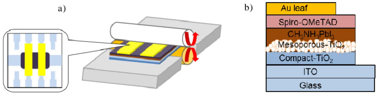
Perovskite solar cells attracted a great deal of attention as solar cells whose power conversion efficiency (PCE) is competitive to that of silicon solar cells[1 ]. Perovskite solar cells have strong light absorption capability and high output voltage and therefore realize the high efficiency[ 2]. In addition, perovskite solar cells have a potential to sign ificantly reduce the production costs, because the devices can be fabricated by simple method such as a spin-coating method and a dip-coating method under atmospheric pressure . However, fabrication of the metal electrodes is generally carried o ut by using a vacuum deposition, which requires an expensive equipment and a long tact time. In order to reduce the production cost and the tact time, it is necessary to develop simple and low cost techniques to fabricate the electrode under a tmospheric pressure. Recently, several techniques have been developed for the fabrication of electrode under of atmospheric pressure such that Ag nanowires[3], Ni mesh/PEDOT:PSS[4 ] or carbon nanotube networks[5 ] as the top electrode. However, the fabrication of these electrodes requires complicated processes with high cost. On the other hand, our group reported that lamination of gold leaf as a top electrode is promising candidate to reduce the cost and tact time to fabricate the electrode for bulk hete ro-junction organic solar cells[6 ]. The PCE of the device using Au leaf electrode approached that of the device using vacuum-evaporated Au electrode. This suggests that, Au leaf electrode formed under optimized lamination conditions can reach the equivalent performance as the device with Au electrode by vacuum deposition. In this study, we applied the Au leaf electrode for perovskite solar cells and investigated the effect of the lamination on the performance of perovskite solar cells. The process temperature and the number of lamination processing were investigated during the lamination process. By forming the electrode with the lamination process, we observed that the crystallinity perovskite effectively improved and the device performance enhanced. We also found that the power conversion efficiency strongly depend on the contact area
2. Methods
2.1 Device fabrication
The schematic of the lamination process and device architecture are shown in Figs. 1a and 1b, respectively. A compact TiO2 layer was formed as follows. First, a 0.15M of TiO2 solution was spin-coated on a cleaned ITO/glass substrate followed by annealing at 130 ºC for 5 min in a glove box. Second, a 0.3M of TiO2 solution was spin-coated on the TiO2 film followed by annealing at 130 ºC for 5 min in a glove box. This process was repeated twice. Finally, the TiO2 layers were annealed at 500 ºC for 20 min in air.Then, a mesoporous-TiO2 layer was formed by spin-coating of TiO2 suspension solution on the compact TiO2 layer in the glove box and annealed at 500 ºC for 30 min in air. A PbI2 solution was spin-coated on the TiO2 layer
2
and followed by annealing at 70 ºC for 1 hour in the glove box. After the annealing of the PbI2 layer, the substrate was immersed in CH3NH3I solution using IPA as a solvent and then annealed at 70 ºC for 1 hour in the glove box. Spiro-OMeTAD solution was spin-coated on the CH3NH3PbI3 perovskite and then annealed at 70 ºC for 30 min. Au leaf (c.a.100 nm) or evaporated Au (100 nm) were used as the Au electrodes of the devices.
For the device with the evaporated the Au electrode, annealing under the pressure with a roller was carried out. Conditions of annealing under the pressure such as the roller speed and the the applied pressure (Pr ol l) were 0.63 cm sec-1 and 0.1 MPa. The roller temperature (Tr oll) was changed 100 and 150 ºC. Number of lamination processing (Nla m) was 3 times. Area of the Au electrode was 0.04 cm2.
The lamination process was carried out to form the Au leaf electrode. The lamination conditions such as the lamination speed and the lamination pressure (Pla m) were 0.63 cm sec-1 and 0.1 MPa. The condition of the roller temperature (Tro ll) was changed 70, 100 and 150 ºC. Number of lamination processing (Nla m) varied 3, 5 and 10 times. Area of the Au leaf electrode was 0.25 cm2.
2.2 Characterization
The current density-voltage (J-V) curve of the devices was measured by a source meter (2400, Keithley) under irradiating AM 1.5 simulated sunlight (100 mW/cm2). The contact area ratio was measured by the color 3D laser microscopy (VK-9710, Keyence).
3. Results and discussion
3.1 Effect of process temperature on the device performance
Figure 2 shows the J-V curves of the devices and the device performances are summarized in Table 1. Fig. 3 shows image of Au leaf surface at each process temperature. Power conversion efficiency of the devices with evaporated Au electrode were improved by annealing under the pr essure. This would be due to the improvement of the crystallinity perovskite[ 7]. Similar improvement of the device performances was observed in the devices with Au leaf electrode. However, PCEs of the devices with Au leaf electrode were lower than thaose of the devices with evaporated Au electrode. Since Series resistance (RS) of the device with Au leaf electrode was about three times higher than that with evaporated Au electrode. Adhesion
Fig. 1 a) The lamination process b) The device architecture
3
between Au leaf electrode and hole transport layer (HTL) is worse in comparison with that between evaporated Au electrode and HTL. As increasing the process temperature, the contact area ratio of between Au leaf electrode and HTL increased from 26.51% to 58.11%.
The highest performances of the devices with Au leaf electrode was observed at the lamination temperature of 150 ºC. On contrary, performances of the devices with evaporated Au electrode was maximized at 100 ºC. This result suggests that the device performances with Au leaf electrode was governed by the adhesion area than that the effect of annealing under pressure to the perovskite layer. Therefore, in the following study, we attempted to improve the contact area ratio by increasing the number of lamination processing while keeping the roller temperature constant at 100 ºC.
3.2 Effect of number of lamination processing on the device performance
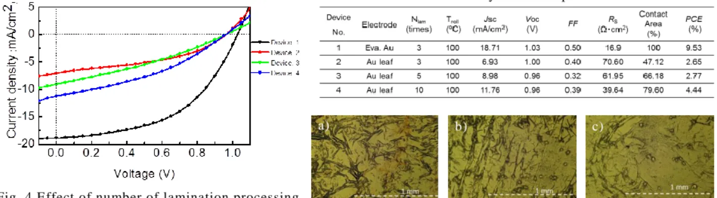
Figure 4 shows the J-V curves of the devices and the device perfor mances are summarized in Table 2. Figure 5 shows image of Au leaf surface at each number of lamination processing.
By increasing the number of lamination processi ng while keeping the roller temperature constant at 100 ºC, the device performances were improved. When the number of lamination processing was 10 times, JS C was greatly increased and RS was decreased. This would be due to the contact area was increased. As a result, PCE of 4.44% and contact area ratio of 79.60% was obtained.
Fig. 2 Effect of process temperature
Table 1 Summary of device performance
Fig. 3 image of Au leaf surface at (a) 70 ºC (b) 100 ºC (c) 150 ºC
4
4. ConclusionsPerovskite solar cells was fabricated with using Au leaf as top electrode . The lamination conditions of the roller temperature and number of lamination processing were optimized. As the roller temperature increases, device performance was improved. However, in contrast to the results of the devices with the evaporated Au electrode, the device with Au leaf electrode reached the maximized PCE by the lamination at 150 ºC. This suggests that the influence of the contact area ratio of between the Au leaf and HTL on the device performance is dominant. When the roller temperature was 100 ºC and number of lamination processing was 10 times, PCE of 4.44% and contact area ratio of 79.60% was obtaine d.
Reference
[1] Effciency Chart, NREL, http://www.nrel.gov/pv/assets/images/efficiency -chart.png (accessed Junuary 22, 2017)
[2] E. Yablonovitch, O. Miller, and S. Kurtz , IEEE Journal of Photovoltaics, 2, 303-311 (2012) [3] F. Guo, et al., Nanoscale, 7, 1642-1649 (2015)
[4] D. Bryant, et al., Adv. Mater., 26, 7499-7504 (2014) [5] Z. Li, et al., ACS Nano, 8, 6797-6804 (2014)
[6] Nur Tahirah Razali, et al., Applied Physics Express, 7, 111602 (2014) [7] J. Xiao, et al., J. Mater. Chem. A, 3, 5289-5293 (2015)
Fig. 4 Effect of number of lamination processing
Table 2 Summary of device performance
Fig. 5 image of Au leaf surface at (a) 3 times (b) 5 times (c) 10 times