perovskite solar cells using the new 3-step
method
著者(英)
Yuji Okamoto
year
2019
その他のタイトル
新規3-step法によるペロブスカイト太陽電池の創製
と高効率化
学位授与大学
筑波大学 (University of Tsukuba)
学位授与年度
2018
報告番号
12102甲第8976号
URL
http://doi.org/10.15068/00156641
Production and efficiency improvement of
perovskite solar cells
using the new 3-step method
Yuji Okamoto
Production and efficiency improvement of
perovskite solar cells
using the new 3-step method
Yuji Okamoto
Doctoral Program in Materials Science
Submitted to the Graduate School of
Pure and Applied Sciences
in Partial Fulfillment of the Requirements
for the Degree of Doctor of Philosophy in
Engineering
at the
The studies presented in this thesis were carried out under the guidance of Associate Professor Yoshikazu Suzuki in the Development of Materials Science at the Graduate School of Pure and Applied Sciences, University of Tsukuba. In this thesis, a new 3-step fabrication method of perovskite solar cell was developed to form bandgap gradients at the both top and bottom sides of perovskite layer.
Perovskite solar cells have attracted much attention, since they can be fabricated by a simple spin-coating method and demonstrate a relatively high power conversion efficiency (PCE). The maximum PCE of perovskite solar cells has recently reached to 23.7%.
For further improvement of PCE, a formation of bandgap gradient at the surface of perovskite light absorbing layer is a promising way. It is effective to improve the PCE by enhancing a carrier transport efficiency. For example, a formation of bandgap gradients at the top and bottom sides has been widely studied for CIGS solar cells, which was carried out by making compositional difference using dry processes. On the other hand, the formation of bandgap gradient at the bottom side is difficult for the perovskite solar cells prepared by a wet-process, e.g., spin-coating, since the compositional difference is usually produced by post-treatments and it can form the bandgap gradient only at the top surface side. Therefore, in this thesis, the new 3-step fabrication method was developed to form the bandgap gradients at the both top and bottom sides of the perovskite layer.
CH3NH3PbI3 (MAPbI3) is generally used as a material for the light absorbing layer of perovskite solar
cells. When the MAPbI3 layer is prepared by a standard 2-step method, i.e. pre-coating of PbI2 layer and
post-conversion to MAPbI3 by reacting with CH3NH3I (MAI), unreacted PbI2 remains at the bottom side. To produce
compositional differences in the perovskite layer, CH(NH2)2I (FAI) solution was additionally spin-coated as
the 3rd step. By the additional spin-coating, the FA concentration difference was produced in the perovskite
layer, and a multiple bandgap structure was successfully obtained by forming the bandgap gradient at the bottom side. Furthermore, the simultaneous formation of bandgap gradients at the both top and bottom sides was also realized by adding trace NaI into the FAI solution. The PCE of perovskite solar cells was effectively improved by the additional spin-coating. The effects of additional spin-coating on crystal structure, composition, film morphology and optical property of perovskite layer were also studied in detail.
Yuji Okamoto February, 2019
i
Chapter 1: Introduction ... 2
1.1 Introduction of solar cells ... 2
1.2 Introduction of perovskite solar cell ... 5
1.2.1 History of perovskite solar cell ... 5
1.2.2 Material for perovskite light absorbing layer (CH3NH3PbI3) ... 6
1.2.3 Structure, working principle, and fabrication method of perovskite solar cell ... 8
1.2.4 Compositional engineering and bandgap gradient structure for perovskite layer ... 11
1.3 Objective of this thesis... 14
References ... 17
Chapter 2: Conversion of unreacted PbI2 into perovskite by an additional MA(I/Br) spin-coating ... 22
2.1 Introduction ... 22
2.2 Experimental ... 22
2.2.1 Preparation method of perovskite solar cell ... 23
2.2.2 Characterizations ... 25
2.3 Results and Discussion ... 30
2.3.1 Phase and crystal structure analysis of perovskite layer ... 30
2.3.2 Optical property analysis and bandgap estimation of perovskite layer ... 32
2.3.3 Microstructure observation of perovskite layer... 34
2.3.4 Evaluations of photovoltaic performance and stability in air ... 36
2.4 Conclusions ... 40
References ... 41
Chapter 3: Formation of multiple bandgap structure at the bottom side of perovskite layer by an additional FAI spin-coating ... 44
3.1. Introduction ... 44
3.2 Experimental ... 45
3.2.1 Preparation method of perovskite solar cell ... 45
3.2.2 Characterizations ... 46
3.3 Results and Discussion ... 47
3.3.1. Phase and crystal structure analysis of perovskite layer ... 47
3.3.2 Optical property analysis and bandgap estimation of perovskite layer ... 48
3.3.3 Microstructure observation of perovskite layer... 50
3.3.4 Detection of multiple bandgap structure ... 52
3.3.5 Evaluation of photovoltaic performance ... 54
3.3.6 Effects of annealing temperature and contact time of FAI solution ... 58
3.4 Conclusions ... 61
Chapter 4: Simultaneous formation of bandgap gradients at the top and bottom sides of perovskite layer by
an additional spin-coating of FAI-NAI solution ... 66
4.1 Introduction ... 66
4.2 Experimental ... 67
4.2.1 Preparation method of perovskite solar cell ... 67
4.2.2 Characterizations ... 69
4.3 Results and Discussion ... 70
4.3.1 Phase and crystal structure analysis of perovskite layer ... 70
4.3.2 Microstructure observation and surface roughness measurement of perovskite layer ... 73
4.3.3 Optical property analysis and bandgap estimation of perovskite layer ... 76
4.3.4 Band structure analysis of perovskite layer ... 77
4.3.5 Evaluations of photovoltaic performance and stability in air ... 80
4.4 Conclusions ... 82
References ... 84
Chapter 5: Summary and Conclusions ... 88
Appendix 1: Perovskite solar cells using BaTiO3/TiO2 double mesoporous layer for electron transport ... 92
A1.1 Introduction ... 92
A1.2. Experimental ... 93
A1.2.1 Preparation of TiO2 and BaTiO3 pastes ... 93
A1.2.2 Preparation method of perovskite solar cell ... 93
A1.2.3 Characterizations ... 94
A1.3 Results and Discussion ... 95
A1.3.1 Microstructure observation of electron transport layer (ETL) ... 95
A1.3.2 Evaluation of photovoltaic performance... 96
A1.3.3 Phase and crystal structure analysis of perovskite layer ... 97
A1.3.4 Microstructure observation of perovskite layer and estimation of particle size distribution ... 97
A1.3.5 Optical property analysis and estimation of bandgap of perovskite layer ... 100
A1.3.6 Evaluation of electron transport efficiency ... 101
A.1.4 Conclusions ... 102
References ... 103
Appendix 2: Perovskite solar cells using SrTiO3/TiO2 composite mesoporous layer for electron transport ... 104
A2.1 Introduction ... 104
A2.2. Experimental ... 104
A2.2.1 Preparation of SrTiO3/TiO2 composite paste ... 104
iii
A2.3 Results and Discussion ... 106
A2.3.1 Microstructure observation of electron transport layer (ETL) and perovskite layer ... 106
A2.3.2 Evaluation of photovoltaic performance... 108
A2.4 Conclusions ... 109
References ...110
Appendix 3: Remote supply of hydrogen radical and production of Si from reduction of SiCl4 ... 111
A3.1 Introduction ... 111
A3.1.1 Conventional production method of high purity Si: Siemens method ... 111
A3.1.2 Potential of hydrogen radical (H-radical) for enhancement of Si yield in Siemens method ... 112
A3.1.3 Requirements to apply H-radical into Siemens method ... 113
A3.1.4 Objective ... 113
Part 1: Generation of H-radical at pressure > 1 atm and transportation ...114
A3.2 Experimental ...114
A3.2.1 Apparatus ... 114
A3.2.2 H-radical generation and transportation ... 114
A3.2.3 Detection of H-radical and evaluation of the density ... 115
A3.3 Results and Discussion ...116
A3.3.1 Effect of generation pressure on H-radical density ... 116
A3.3.2 Effect of applied current to W filaments (filament temperature) on H-radical density ... 118
A3.3.3 Effect of distance from H-radical generation chamber to detection point on H-radical density... 118
A3.4 Conclusions ...119
Part 2: Production of Si from reduction of SiCl4 by H-radical at 1 atm ... 120
A3.5 Experimental ... 120
A3.5.1 Apparatus ... 120
A3.5.2 Reduction of SiCl4 by H-radical ... 121
A3.5.3 Characterizations ... 121
A3.6 Results and Discussion ... 121
A3.6.1 Reduction of SiCl4 by H-radical at the reaction pressure of ~1.8 kPa ... 121
A3.6.2 Reduction of SiCl4 by H-radical at the reaction pressure of 1 atm ... 124
A3.7 Conclusions ... 127
References ... 128
Achievements ... 130
1
Chapter 1
2
Chapter 1: Introduction
1.1 Introduction of solar cells
Recently, an introduction amount of photovoltaic power system has increased due to an issue of global warming mainly caused by CO2 emission [1,2]. Therefore, a further improvement of the conversion efficiency
of solar cells is necessary. Besides the most popular silicon (Si) based solar cells, there are a variety of solar cells. The classification of solar cells is shown in Fig. 1.1, and the maximum power conversion efficiency (PCE) of these solar cells is shown in Fig. 1.2. Solar cells can be classified into Si based type, compound type, organic type, quantum dot type, and organic/inorganic hybrid type.
Fig. 1.1 Classification of solar cells [3]. Single crystalline Si based solar cells
This solar cell uses a monocrystalline Si as the raw material, and the maximum power conversion efficiency (PCE) at the laboratory level is currently 26.1% [4]. A relatively high PCE of ~16-20% can be obtained even for the commercial modules [5]. However, the production cost is relatively high compared with the other solar cells since a large single crystal Si substrate is required to produce a module. Recently, the production cost has been reduced thanks to progresses of the production technology, and its market share among the various solar cells is increasing.
Polycrystalline Si based solar cells
3
production cost is lower than that of single crystalline Si solar cell, but the PCE is lower. However, the share of the polycrystalline Si based solar cell is the highest in the solar cell market.
Amorphous Si based solar cells
This solar cell uses an amorphous Si as the row material. The maximum PCE is 14.0% [4]. Since the optical absorption coefficient of amorphous silicon is larger than that of single crystal silicon, a thin film type solar cell can be produced, which is effective to reduce the consumption of Si. The PCE is lower than those of crystalline Si solar cells.
Hetero-junction type (HIT) Si solar cells
This solar cell is composed of a heterojunction of crystalline Si and amorphous Si. It is called HIT (Hetero-junction with Intrinsic Thin Layer) type Si solar cells. The single crystalline Si is sandwiched by the amorphous Si. The maximum PCE is 26.6% [4]. It has a higher voltage, PCE and thermal stability than single crystal silicon solar cell. However, the production cost is higher due to the multijunction structure.
Compound type solar cells
This solar cell uses the compound of more than two elements as the raw material, such as groups II-IV and groups III-V in a periodic table. Since the bandgap is controlled by the combination of materials, a relatively high PCE can be obtained. In addition, they have large light absorption coefficients, so thin film type solar cells can be produced. There are several types of the compound type solar cells, such as CdTe (maximum PCE: 22.1% [4]), CIS (CuInSe2), CIGS (Cu(In, Ga)Se2), maximum PCE: 22.9% [4]), and GaAs types.
Quantum dot type solar cells
This solar cell uses a quantum dot as the row material. The size of particles used for the light absorbing layer is reduced to nanometer size. Since the absorbing light-wavelength can be tuned by changing the size of the quantum dot, a theoretical PCE is expected to be over ~ 63%. The maximum PCE is currently 16.6% [4]. Organic type solar cells
This solar cell is composed of organic electron donor layer and organic hole acceptor layer. This structure is similar to a p-n junction of an inorganic type solar cell. The PCE was ~1% in 2000, but the maximum PCE is currently 15.6% [4]. Although the PCE is still smaller than those of the other inorganic type solar cells, the production cost can be lower.
Organic/inorganic hybrid solar cells
This solar cell consists of a combination of organic and inorganic materials, and fabrication techniques of both organic and inorganic solar cells are used. There are basically two organic/inorganic hybrid solar cells, i.e. dye-sensitized solar cells and perovskite solar cells. This thesis focuses on the perovskite solar cells. The details will be described in the next section.
4
5
1.2 Introduction of perovskite solar cell 1.2.1 History of perovskite solar cell
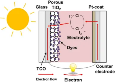
The perovskite solar cell was developed based on the dye-sensitized solar cells, so it is better to describe about the dye-sensitized solar cells firstly. In the dye-sensitized solar cells, organic dyes are fixed on an oxide mesoporous layer. The dyes absorb the light which cannot be absorbed by the oxide semiconductor (dye-sensitization) and generate electrons [6]. In 1991, Prof. Grätzel’s group firstly reported the dye-sensitized solar cells [7]. The cell had a transparent conductive oxide (TCO) glass, TiO2 mesoporous layer prepared on the
TCO glass, and organic dyes fixed on the TiO2 mesoporous layer. They were sandwiched by the other TCO
glass, and an electrolyte was injected into the gap of TCO glasses (Fig. 1.3). Under the sun light irradiation, the organic dyes are excited and emit electrons. The electrons are transported to outside through the conduction band of TiO2, and electricity is generated. The PCE was ~7% in the first report [7], but the PCE of ~10 % was
reported in 1993 [8]. After that, the dye-sensitized solar cells attracted much attention as a new generation low-cost solar cell, since it had a relatively high PCE of over 10% in spite of its easy fabrication process. The PCE was gradually increased and the maximum PCE is currently 11.9% [4].
Fig. 1.3 Structure and working principle of dye-sensitized solar cells.
In the meantime, Prof. Miyasaka’s group reported a unique dye-sensitized solar cell which used organometal trihalide perovskite: CH3NH3PbX3 (X= I or Br) as the sensitizer in 2009 [9]. They prepared the
light absorbing layer using CH3NH3PbX3 in the TiO2 mesoporous layer, and PCE of 3.8% was achieved.
However, there was a problem on the stability due to a dissolution of CH3NH3PbX3 in the electrolyte, which
resulted in the degradation of the PCE. In 2012, Prof. Park’s group used a solid-state hole transport layer (HTL, spiro-MeOTAD) instead of the electrolyte to solve the problem, and they obtained the PCE of 9.7% [10]. Furthermore, Lee et al. [11] reported the PCE of 10.9% by using a mesoporous Al2O3 layer and the
spiro-MeOTAD based HTL in the same year. These reports gave a big impact on the researchers, since the maximum PCE comparable to that of dye-sensitized solar cells was achieved just in 3 years from the first report. After that, many researchers started to work on the perovskite solar cell, and the cell structure, preparation method, and composition of materials have been widely studied.
6
At the initial stage of the research, this solar cell was regarded as one of the dye-sensitized solar cells. However, it generated the PCE of 10.9% even with the Al2O3 mesoporous layer which does not transport the
electrons [11]. This is significantly different characteristics from the dye-sensitized solar cells. Therefore, this solar cell is recently regarded as a new category of the solar cell, and it is called as a “perovskite solar cell”. The maximum PCE of the perovskite solar cell already reached to 23.7% [4], which is close to that of the single crystalline Si solar cells, recorded in just 9 years from the first report. This rapid increase of PCE is a feature of perovskite solar cells. Since the research on upsizing of the perovskite solar cells has already started, a productization of this solar cell can be expected [12].
1.2.2 Material for perovskite light absorbing layer (CH3NH3PbI3)
Methyl-ammonium lead iodide: CH3NH3PbI3
Methyl-ammonium lead iodide (CH3NH3PbI3, MAPbI3) has been widely used as a material for the light
absorbing layer of the perovskite solar cells. It is an organic/inorganic hybrid perovskite ionic crystal. Perovskite is a mineral name of calcium titanate (CaTiO3), which was named after Russian scientist “Perovsky”
who discovered the mineral CaTiO3. Currently, the crystal structure of CaTiO3 represented by ABX3 is called
as a perovskite structure, and there are many functional materials which have the perovskite structure, such as ferroelectric BaTiO3 and Pb(Zr,Ti)O3 [13].
Figure 1.4 shows a crystal structure of a cubic perovskite-type structure. The ideal perovskite-type structure has a cubic unit cell (e.g. SrTiO3), but there are also many compounds with lower symmetry unit cells
(ex. tetragonal and orthorhombic). The tolerance factor is a factor which shows stability and distortion of the perovskite structure. The tolerance factor t is given by the eq. 1.1, where rA, rB, and rX are the ionic radii of the
ions located in A, B and X sites, respectively.
tolerance factor (t) = (𝑟 + 𝑟 ) / √2 (𝑟 + 𝑟 ) (eq. 1.1) The tolerance factor must be within ~0.8-1.1 to form the perovskite structure. When t = 1, the crystal structure has a cubic unit cell, and when t < 1 or t >1, the crystal structure is distorted into tetragonal, orthorhombic, or rhombohedral unit cell.
7
CH3NH3PbI3 has the perovskite structure, and the A, B, and X sites are occupied by CH3NH3+, Pb2+, and
I- ions, respectively. The crystal phase changes by the temperature. In 1987, Politsch et al. [15] reported that
CH3NH3PbI3 has an orthorhombic phase at T < 162 K (P na21, low temperature phase), tetragonal phase at 162
K < T < 327 K (I 4/mcm, room temperature phase), and cubic phase at 327 K < T (Pm3m, high temperature phase). On the other hand,Stoumpos et al. [16] recently reported that CH3NH3PbI3 has tetragonal phase of (P
4mm) and (I 4cm) for the high temperature phase and room temperature phase, and orthorhombic phase (Pnma) for the low temperature phase. Figure 1.5 shows crystal structures of CH3NH3PbI3 for the cubic, tetragonal,
and orthorhombic phases. According to the study by Oku et al. [17], the lattice parameters of orthorhombic phase are a = 8.8362 Å, b = 12.5804 Å, c = 8.5551 Å, those for tetragonal phase are a = 8.800 Å, c = 12.685 Å, and that for cubic phase is a = 6.391 Å.
Fig. 1.5 Crystal structures of CH3NH3PbI3 for cubic, tetragonal, and orthorhombic phases (drown by VESTA
ver. 3.4.4 [14]).
Characteristics of CH3NH3PbI3
CH3NH3PbI3 has desirable characteristics as a light-absorbing layer of solar cell. Firstly, the preparation
process of CH3NH3PbI3 layer is very simple. The CH3NH3PbI3 layer can be formed just by spin-coating a
precursor solution and annealing at a temperature of ~100°C. Since the annealing temperature is relatively low, it is possible to form the CH3NH3PbI3 layer on a plastic film substrate and to produce a flexible perovskite
solar cell (Fig. 1.6(a) [18]). Also, a large-scale vacuum equipment is not necessary unlike the inorganic type solar cells, so the CH3NH3PbI3 film can be fabricated with low cost. Secondary, the bandgap value is suitable
to absorb the entire visible light in the sun light. The bandgap of CH3NH3PbI3 is reported to be ~1.5-1.6 eV
[10,19] which can absorb the most of the visible light: < ~800 nm. Since the sun light has the largest light intensity at the visible light region, CH3NH3PbI3 can absorb the sun light and generate electrons efficiently.
Thirdly, a light absorption coefficient is high: ~105 cm-1 (Fig. 1.6 (b) [20]), which is equivalent to those of
inorganic semiconductors such as Si and CIGS. This high absorption coefficient enables to absorb the most of visible light with a film thickness of several hundred nanometers. Fourthly, the CH3NH3PbI3 has a very long
carrier diffusion length. The carrier diffusion length of CH3NH3PbI3 was reported to be ~100 nm, and it can be
further prolonged to ~1 μm by mixing Cl- into the X site (CH
3NH3PbI3-xClx) [21]. Since the thickness of the
8
Figs. 1.6 (a) Appearance of flexible perovskite solar cell reported by Giacomo et al. [18], and (b) comparison of absorbance coefficients reported by Xie et al. [20].
1.2.3 Structure, working principle, and fabrication method of perovskite solar cell Structure of perovskite solar cells
The perovskite solar cell has three layers to generate and transport carriers (electrons and holes), a perovskite light absorbing layer, an electron transport layer (ETL), and a hole transport layer (HTL). The perovskite light absorbing layer is sandwiched by the ETL and HTL. The structures can be categorized into three types by the usage of the ETL and HTL. The three structure types are shown in Fig. 1.7.
(1) Mesoporous structure
This structure is composed of a TCO glass, ETL, perovskite layer, HTL, and metal electrodes. Oxide semiconductors, such as TiO2, SnO2, and ZnO, are usually used for the ETL. The spiro-MeOTAD
([2,2',7,7'-Tetrakis(N,N-di-p-methoxyphenylamino)-9,9'-spirobifluorene] is widely used for the HTL, and gold (Au) or silver (Ag) are used for the metal electrodes. In the mesoporous structure, the ETL is composed of compact and mesoporous layers. A part of perovskite film is infiltrated into the mesoporous layer, and the other part forms a perovskite capping layer. In this thesis, this mesoporous structure was used.
As described in section 1.2.1, the perovskite solar cell was developed based on the dye-sensitized solar cell. Since the dye-sensitized solar cells used a TiO2 mesoporous layer for the electron transport, the
mesoporous structure was used at the beginning of research on perovskite solar cells. At that time, it was believed that the generated electrons must be injected into the mesoporous TiO2 layer in the same way as the
dye-sensitized solar cells. However, in 2012, a PCE > 10% was reported with the Al2O3 mesoporous layer [11].
This result indicated that CH3NH3PbI3 can separate and transport the carriers (electrons and holes) by itself,
since Al2O3 cannot transport the electrons due to its too high conduction band level. The perovskite solar cells
do not always need the mesoporous layer for the electron transport. Because of these reasons, the planar structure was developed.
(2)&(3) Planar and inverted planar structure
9
the mesoporous structure, it is beneficial to reduce the production cost and to investigate the mechanisms of this solar cell. The thickness of the perovskite layer is usually less than ~500 nm due to the high optical absorption coefficient of CH3NH3PbI3, and CH3NH3PbI3 has the long carrier diffusion length of ~100 nm-1
μm. Therefore, the generated carriers in the perovskite layer can reach to the compact layer (ETL) by itself without the mesoporous layer, which realizes the planar structure. Recently, the structure without HTL was also reported [24,25]. The other type is an inverted planar structure. This structure has the ETL and HTL in opposite positions to those of the normal planar type structure [26,27]. [6,6]-phenyl C61-butyric acid methyl ester (PCBM) and fullerene (C60) are widely used for the ETL, and poly(3,4-ethylenedioxythiophene) poly(styrene‐sulfonate) (PEDOT: PSS) and NiO are used for the HTL.
Fig. 1.7 Three types structure of perovskite solar cells. Working principle of the perovskite solar cells
Figure 1.8 shows the working principle of the perovskite solar cells. The model is based on the mesoporous-type perovskite solar cells. Under the sun light irradiation from the TCO glass side, the perovskite layer is exited and emits the electrons and holes. The electrons and holes are transported to outside through the conduction band (CB) of ETL (TiO2) and the highest occupied molecular orbital (HOMO) level of the HTL
(spiro-MeOTAD), respectively. Therefore, the position of the conduction band of ETL and the HOMO level of HTL are important for the electron and hole transports. The CB level of ETL and HOMO level of HTL should be lower and higher than the CB and valence band (VB) levels of CH3NH3PbI3, respectively.
10
Fabrication method of perovskite layer
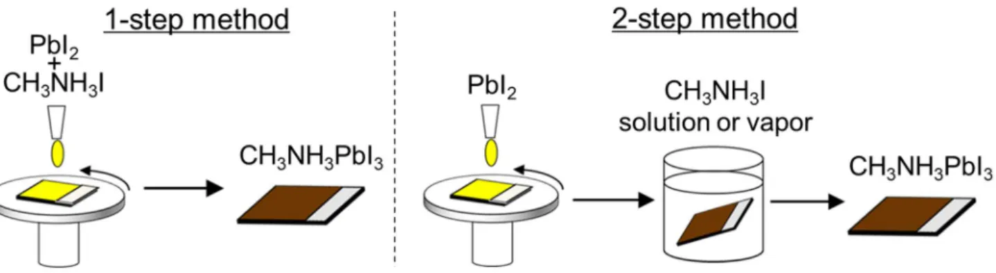
The perovskite light absorbing layer (CH3NH3PbI3) is generally fabricated by reacting PbI2 and CH3NH3I
(MAI). In general, the preparation methods are categorized into two methods: 1-step method and 2-step method (Fig. 1.9). In the 1-step method, the CH3NH3PbI3 layer is prepared by one-step spin-coating of a precursor
solution composed of PbI2 and CH3NH3I. Since this method is simpler than the 2-step method, it is suitable for
the low-cost production. However, if the spin-coating conditions or the compositions of precursor solution are not optimized, it is difficult to obtain a well-covered perovskite layer on the ETL [22,28]. To solve this problem, an anti-solvent dripping method was developed [29,30]. By spin-coating a poor solvent, such as toluene and chlorobenzene, just after the spin-coating of perovskite precursor solution, the nucleation of CH3NH3PbI3 is
significantly accelerated, and a smooth and compact perovskite layer can be obtained. However, this method is very sensitive to the process conditions, such as the amount of poor solvent and timing of the spin-coating, so the handling is difficult.
On the other hand, in the 2-step method, the PbI2 film is firstly prepared, and CH3NH3I post-treatment
using solution or vapor is secondary carried out to synthesize the CH3NH3PbI3. The 2-step method requires
another step compared with the 1-step method, but it is relatively easy to obtain well-covered perovskite layer. However, the 2-step method still has a problem as described below. Thus, in this thesis, the 2-step method was mainly focused.
Fig. 1.9 Schematic illustration of 1-step and 2-step methods for the preparation of perovskite layer. Problem of the 2-step method
In the 2-step method, the PbI2 layer is firstly prepared and then it reacts with CH3NH3I to obtain
CH3NH3Pb13. Since CH3NH3PbI3 is formed from the surface of PbI2 layer, the diffusion of CH3NH3I into the
deep part of the PbI2 layer is gradually hindered, and this causes a residual unreacted PbI2 at the bottom of the
perovskite layer (Fig. 1.10) [31,32].
11
Some improved processes were proposed to solve this problem, e.g., solvent selection and morphological control of PbI2 layer. At the begging of the research, N,N-dimethylformamide (DMF) was usually used as a
solvent of PbI2 solution. When DMF is used as the solvent, the formed PbI2 layer is well-crystalized during
the annealing, and it makes difficult for CH3NH3I to diffuse into the deep part of PbI2 layer. To suppress the
crystallization of PbI2 layer, dimethyl sulfoxide (DMSO) was used as the solvent. Since DMSO forms a
complex with PbI2, the crystallization of PbI2 layer was suppressed and the reaction with CH3NH3I was
prompted. As a result, the unreacted PbI2 was suppressed and photovoltaic performance was improved [33,34].
The second approach was to form a mesoporous PbI2 layer. The conventional PbI2 layer using DMF as the
solvent was a relatively dense film. Cao et al. [35] prepared a mesoporous PbI2 layer by using a molecular
level pore-forming agent. The mesoporous structure facilitated the penetration of CH3NH3I into the deep part
of the PbI2 layer, and the CH3NH3PbI3 layer without unreacted PbI2 was achieved with the enhanced
photovoltaic performance.
On the other hand, it was also reported that the unreacted PbI2 was beneficial to achieve the better
photovoltaic performance. Since the conduction band of PbI2 is located at higher position than that of
CH3NH3PbI3, the unreacted PbI2 is effective to suppress the back-flow of the electrons and to suppress a carrier
recombination [31]. Therefore, it is still unclear that the complete elimination of unreacted PbI2 has positive
or negative effect on the photovoltaic performance. Still, the author of this thesis thinks that the reduction of unreacted PbI2 amount is a key to obtain a high PCE.
1.2.4 Compositional engineering and bandgap gradient structure for perovskite layer
Compositional engineering of perovskite layer
Since CH3NH3PbI3 has a perovskite structure (ABX3), when Pb2+ in the B site is fixed, it is possible to
change the monovalent cation in the A site and the halogen ion in the X site. The replacement of the ions changes the lattice constant and bandgap of the material, which is effective to improve the photovoltaic performance and stability. Formaminidium ion (CH(NH2)2+, FA+) and Cs+ ions have been widely used for the
substitution of A site. Cl- and Br- are used for the substitution of halogen ion in the X site. Table 1.1 summarizes
the tolerance factors and bandgaps of the perovskite materials when the ion in the A site (CH3NH3+) is replaced
with Cs+ or FA+ ion and the ion in X site (I-) is replaced with Cl- or Br- ion. The ionic radius of Pb2+ is 1.19 Å
[36].
The tolerance factor approaches to 1 and the band gap becomes smaller by using larger cations for the A site. For example, FAPbI3 has a tolerance factor of 0.987 and a bandgap of 1.47 eV [37], which is closer to the
optimal bandgap value of 1.4 eV for the solar cell application. As for the anion substitution,the tolerance factor approaches to 1 by using smaller anion for the X site, and the smaller anions give the larger bandgaps. In this way, the bandgap can be tuned by the compositional engineering.
12
Table 1.1 Ionic radius, tolerance factor and bandgap of perovskite materials when Pb2+ in the B site is fixed
and ions for the A site and X site are varied.
A site cation Cs+ MA+ (CH 3NH3+) FA+ (CH(NH2)2+) Ionic radius (Å) 1.88[36] 2.17[38] 2.53[38] Tolerance factor (APbI3) 0.851 (CsPbI3) 0.912 (MAPbI3) 0.987 (FAPbI3) Bandgap (eV) (APbI3) 1.73 (CsPbI3) [39] 1.5-1.6 (MAPbI3)[10.19] 1.47 (FAPbI3)[37] X site anion Cl- Br- I -Ionic radius (Å) 1.81[36] 1.96[36] 2.20[36] Tolerance factor (MAPbX3) 0.938 (MAPbCl3) 0.927 (MAPbBr3) 0.912 (MAPbCl3) Bandgap (eV) (MAPbX3) 3.11 (MAPbCl3)[40] 2.29 (MAPbBr3)[41] 1.5-1.6 (MAPbI3)
Cesium lead iodide (CsPbI3)
CsPbI3 has better thermal and air stability than CH3NH3PbI3. The α-phase CsPbI3 has the perovskite
structure and bandgap of 1.73 eV which is also suitable for a top cell of the tandem solar cell with Si. However, δ-CsPbI3 (non-perovskite structure, yellow color, bandgap: 2.82 eV [39], not suitable for solar cell application)
is also synthesized, since it is more stable than α-phase CsPbI3 at room temperature (T < 315°C), which
decreases the PCE [42].
Formamidinium lead iodide (FAPbI3)
FAPbI3 has better thermal stability than CH3NH3PbI3. The α-phase FAPbI3 has a bandgap of 1.47 eV
which is closer to the optimal bandgap value of 1.4 eV as the solar cell application. However, δ-FAPbI3
(non-perovskite structure, yellow, bandgap: 2.43 eV [43]) is also synthesized, since it is more stable than α-phase FAPbI3 at room temperature, which decreases the PCE.
Both δ-CsPbI3 and δ-FAPbI3 are stable at room temperature, and hence, the stabilization of α-phase at
room temperature is a challenging research topic. The incorporation of other cation and anion is a way to achieve the stable α-phase. For example, the tolerance factor approached to 1 by incorporating the smaller Br
-ion to CsPbI3, and the formation of δ-CsPbI3 can be suppressed. It is also reported that the formation of
δ-FAPbI3 is suppressed by incorporating MA+ and Br- ions due to the change of lattice constant and relaxation
of the lattice strain [44,45].
Methyl-ammonium lead chloride (CH3NH3PbCl3)
CH3NH3PbCl3 has a too large bandgap for the solar cell application, so pure CH3NH3PbCl3 is usually not
13
Methyl-ammonium lead bromine (CH3NH3PbBr3)
CH3NH3PbBr3 also has a too large bandgap for the solar cell application, so pure CH3NH3PbBr3 is usually
not used for the light absorbing layer. However, the incorporation of Br- into the I- based perovskite layer is
widely studied. By incorporating the Br-, the bandgap becomes larger, which results in an increase of open
circuit voltage (VOC) and decrease of short circuit current density (JSC). Furthermore, since the structure
changes from the tetragonal to the cubic structure and tolerance factor also approaches to 1 by the Br
-incorporation, the air stability can be improved [41].
As described above, when each material is used for the perovskite light absorbing layer as a pure phase, there are some problems. However, by combining the materials, the advantage of each material can be achieved without crucial negative effects. Therefore, the mixed composition of these ions has recently studied to achieve the both high PCE and stability. For example, (MAFA)Pb(IBr) or (CsMAFA)Pb(IBr) system-based perovskite solar cells achieved a PCE of ~20% with higher stability than those pure composition-based perovskite solar cells [46,47].
Bandgap gradient structure
The generated electrons and holes in the perovskite light absorbing layer are transported through conduction band and valence band (HOMO level for HTL) of each layer as shown in Fig. 1.8, and hence, the band alignment is important factor to achieve high photovoltaic performance. The importance of band alignment is applied not only for the perovskite solar cells but also for all kinds of solar cells, since they have a similar mechanism of the carrier transport.
As for the light absorbing layer, a formation of bandgap gradient is a promising way to enhance the photovoltaic performance. For example, the formation of bandgap gradient structure at the front and back side of CIGS (Cu, In, Ga, Se) light absorbing layer has been widely studied by changing the Ga ratio or by substituting Se with S [48,49]. Since the bandgap gradient is a driving forth of the carrier transport, the carrier transport efficiency is improved and the photovoltaic performance is also enhanced.
In the case of perovskite solar cells, some researchers reported the formation of bandgap gradient at the top surface side of the perovskite layer, which resulted in the enhanced photovoltaic performance. Cho et al. [50] and Kim et al. [51] formed the I-Br anionic gradient structures by making Br rich area at the top surface side (Fig. 1.11). Since CH3NH3PbBr3 has the larger bandgap and the valence band position is located at the
lower position than those of CH3NH3PbI3, the bandgap gradient can be obtained. It effectively suppressed the
carrier recombination by improving a hole extraction at the top surface side, which resulted in the improved photovoltaic performance. Thus, the formation of bandgap gradient is a promising way to enhance the maximum conversion efficiency of the perovskite solar cells.
14
Fig. 1.11 Schematic illustration of a formation of bandgap gradient by making I-Br concentration gradient reported by Kim et al. [51].
For further advancement on the bandgap gradient structure of perovskite solar cells, it is necessary to form the bandgap gradient at the bottom side of perovskite layer. The formation of bandgap gradient at the bottom side is relatively easy when the perovskite layer is formed layer by layer using dry processes, such as chemical vapor deposition (CVD) and sputtering, but the dry process will increase the production cost. On the other hand, the formation of bandgap gradient at the bottom side by wet processes, such as spin-coating and dipping method, is difficult, since the compositional difference is produced by post-treatments and it can form the bandgap gradient only at the top surface side. Therefore, the new preparation method of perovskite layer which can control the band structure of both top and bottom sides is necessary for further enhancement of the photovoltaic performance.
1.3 Objective of this thesis
From these backgrounds, in this thesis, the author attempted to form the bandgap gradients at the both top and bottom sides of the perovskite layer (multiple bandgap structure) by making compositional differences. To achieve the structure, the author proposes a new 3-step method using additional MAI or FAI spin-coating. In this method, the unreacted PbI2 was used as a material to produce the compositional difference at the bottom
side. The additional FAI spin-coating will convert MAPbI3 into FAxMA1-xPbI3 and it will also convert the
unreacted PbI2 into FA rich layer (FAPbI3 or FAyMA1-yPbI3 (y > x)). Since FAPbI3 has the smaller bandgap than
MAPbI3, the FA concentration difference will make the bandgap gradient at the bottom side.
The objectives of this thesis are to develop a new 3-step method which enables to form the bandgap gradients at the both top and bottom sides of the perovskite layer and enhance the photovoltaic performance of perovskite solar cells. This thesis consists of following chapters.
15
In Chapter 2, the conversion of unreacted PbI2 in the 2-step prepared perovskite layer was carried out by
the 3-step method using MAI additional spin-coating (Fig. 1.12). Also, a compositional change was also attempted by the additional spin-coating of a MABr solution. The conversion of the unreacted PbI2 and
compositional change were analyzed by X-ray diffraction (XRD), and the effects of additional spin-coating on the optical property and film morphology were evaluated byultraviolet-visible absorption spectroscopy (UV-Vis) and scanning electron microscopy (SEM), respectively. The solar cell performances were evaluated by measuring current density-voltage (J-V) characteristics of the prepared cells.
Fig. 1.12 Schematic illustration of the 3-step method using additional MAI spin-coating for conversion of unreacted PbI2 into perovskite.
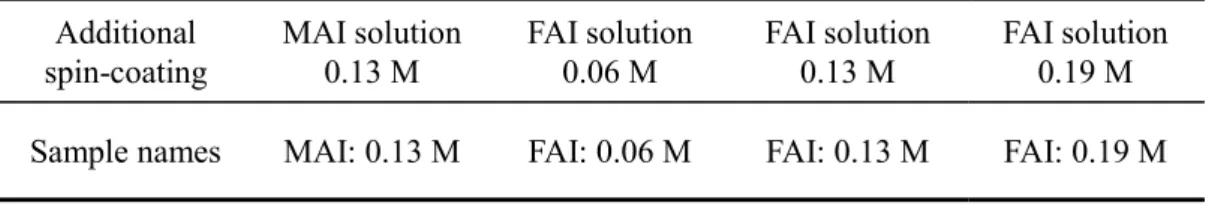
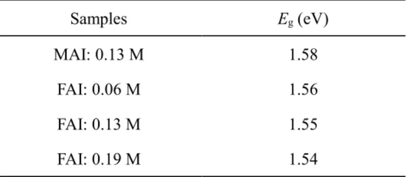
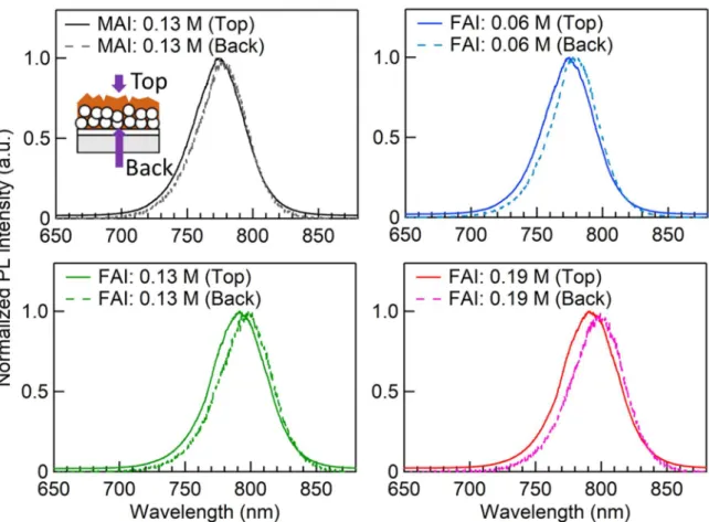
In Chapter 3, the multiple bandgap structure was formed by making the bandgap gradient at the bottom side (near the ETL). The compositional difference was produced by the 3-step method using additional FAI spin-coating on the 2-step prepared perovskite layer (Fig. 1.13). Since the expected FA rich area was too thin to be detected by XRD or UV-Vis, steady-state photoluminescence (PL) measurement was carried out from the top and back sides of the perovskite layer. The effect of additional FAI spin-coating on the photovoltaic performance was also investigated.
Fig. 1.13 Schematic illustration of the 3-step method using additional FAI spin-coating for formation of multiple bandgap structure at the bottom side of perovskite layer.
In Chapter 4, the small amount of NaI was added into the 3rd step FAI spin-coating solution to form the
bandgap gradients at the both top and bottom sides of the perovskite layer simultaneously (Fig. 1.14). The small amount of Na+ in the 3rd step solution will be doped only at the top side of the perovskite layer, and it
will enlarge the bandgap at the top surface with keeping the bandgap gradient at the bottom side. The effects of NaI addition on the bandgap, film morphology, and photovoltaic performance were also investigated.
16
Fig. 1.14 Schematic illustration of the 3-step method with NaI addition for simultaneous formation of bandgap gradients at the top and bottom sides of perovskite layer.
17
References
[1] Ministry of Economy, Trade and Industry, Agency for Natural Resources and Energy, FY2017 Annual Report on Energy (Energy White Paper 2018) PDF version, Part 2 Energy Trends, Chapter 1 Domestic Energy Trends (in Jpn.).
[2] Ministry of Economy, Trade and Industry, Agency for Natural Resources and Energy, FY2017 Annual Report on Energy (Energy White Paper 2018) PDF version, Part 2 Energy Trends, Chapter 2 International Energy Trends (in Jpn.).
[3] K. Sato, Ichiban yasashi rikokei Basic of solar cell, Softbank Creative, (in Jpn., 2011/4/23).
[4] Research Cell Record Efficiency Chart by The National Renewable Energy Laboratory, https://www.nrel. gov/pv/assets/pdfs/pv-efficiencies-07-17-2018.pdf, (2018/12/24).
[5] M. Yamaguchi, M. A. Green, Y. Ohshita, N. Kojima, Fundamentals and applications of solar cells from silicon to organic and quantum nano, Maruzen Publishing Co.,Ltd., (2010/07/30, in Jpn.).
[6] H. Arakawa, Dye-sensitized solar cells, CMC Publishing Co.,Ltd., (2001/5/25, in Jpn.).
[7] B. O’Regan, M. Grätzel, A low-cost, high-efficiency solar cell based on dye-sensitized colloidal TiO2 films,
Nature, 353, 737-740 (1991).
[8] M. K. Nazeeruddin, A. Kay, I. Rodicio, R. Humphry-Baker, E. Mueller, P. Liska, N. Vlachopoulos, M. Graetzel, Conversion of light to electricity by cis-X2bis(2,2'-bipyridyl-4,4'-dicarboxylate)ruthenium(II)
charge-transfer sensitizers (X = Cl-, Br-, I-, CN-, and SCN-) on nanocrystalline TiO2 electrodes, J. Am.
Chem. Soc., 115, 6382-6390 (1993).
[ 9 ] A. Kojima, K. Teshima, Y. Shirai, T. Miyasaka, Organometal halide perovskites as visible-light sensitizers for photovoltaic cells, J. Am.Chem. Soc., 131, 6050-6051 (2009).
[10] H. S. Kim, C. R. Lee, J. H. Im, K.B. Lee, T. Moehl, A. Marchioro, S. J. Moon, R. Humphry-Baker, J. H. Yum, J. E. Moser, M. Grätzel, N.G. Park, Lead iodide perovskite sensitized all-solid-state submicron thin film mesoscopic solar cell with efficiency exceeding 9%, Sci Rep. 2, 591 (2012).
[11] M. M. Lee, J. Teuscher, T. Miyasaka, T. N. Murakami, H. J. Snaith, Efficient hybrid solar cells based on meso-superstructured organometal halide perovskites, Science, 42, 643-647, (2012).
[12] Y. Chen, L. Zhang, Y. Zhang, H. Gaoa, H. Yan, Large-area perovskite solar cells – a review of recent progress and issues, RSC Adv., 8, 10489–10508.
[13] T. R. Shrout, S. J. Zhang, Lead-free piezoelectric ceramics: Alternatives for PZT?, J. Electroceram. 19, 113–126 (2007).
[ 14 ] K. Momma, F. Izumi, "VESTA 3 for three-dimensional visualization of crystal, volumetric and morphology data, J. Appl. Crystallogr., 44, 1272-1276 (2011).
[15] A. Poglitsch, D. Weber, Dynamic disorder in methylammoniumtrihalogenoplumbates (II) observed by millimeter‐wave spectroscopy, J. Chem. Phys., 87, 6373-6378 (1987).
[16] C. C. Stoumpos, C. D. Malliakas, and M. G. Kanatzidis, “Semiconducting tin and lead iodide perovskites with organic cations: Phase transitions, high mobilities, and near-infrared photoluminescent properties, Inorg. Chem., 52, 9019- (2013).
[17] T. Oku, Crystal structures of CH3NH3PbI3 and related perovskite compounds used for solar cells, Solar
Cells - New Approaches and Reviews ed L A Kosyachenko (InTech), 77, chapter 3 (2015).
[18] F. D. Giacomo, V. Zardetto, A. D'Epifanio, S. Pescetelli, F. Matteocci, S. Razza, A. D. Carlo, S. Licoccia, W. M. M. Kessels, M. Creatore, T. M. Brown, Flexible perovskite photovoltaic modules and solar cells based on atomic layer deposited compact layers and UV-irradiated TiO2 scaffolds on plastic substrates,
Adv. Energy Mater. 1401808 (2015).
[19] H. S. Jung, N. G. Park, Perovskite solar cells: from materials to devices, small, 11, 1 (2015).
[20] Z. Xie, S. Sun, Y. Yan, L. Zhang, R. Hou, F. Tian, G. G. Qin, Refractive index and extinction coefficient of NH2CH = NH2PbI3 perovskite photovoltaic material, J. Phys.: Condens. Matter., 29, 245702 (2017).
[21] S. D. Stranks, G. E. Eperon, G. Grancini, C. Menelaou, M. J. P. Alcocer, T. Leijtens, L. M. Herz, A. Petrozza, H. J. Snaith, Electron-hole diffusion lengths exceeding 1 micrometer in an organometal trihalide
18
perovskite absorber, Science, 342, 341–344 (2013).
[22] G. E. Eperon, V. M. Burlakov, P. Docampo, A. Goriely, H. J. Snaith, Morphological control for high performance, solution-processed planar heterojunction perovskite solar cells, Adv. Funct. Mater., 24, 151– 157 (2014).
[23] M. Liu, M. B. Johnston, H. J. Snaith, Efficient planar heterojunction perovskite solar cells by vapour deposition, Nature, 501, 395–398 (2013).
[24] A. Mei, X. Li, L. Liu, Z. Ku, T. Liu, Y. Rong, M. Xu, M. Hu, J. Chen, Y. Yang, M. Grätzel, H. Han, A hole-conductor–free, fully printable mesoscopic perovskite solar cell with high stability, Science 345, 295-298 (2014).
[25] S. Aharon, S. Gamliel, B. E. Cohen, L. Etgar, Depletion region effect of highly efficient hole conductor free CH3NH3PbI3 perovskite solar cells. Phys. Chem. Chem. Phys. 16, 10512-10518 (2014).
[ 26 ] J. Y. Jeng, Y. F. Chiang, M. H. Lee, S. R. Peng, T. F. Guo, P. Chen, T. C. Wen, CH3NH3PbI3
perovskite/fullerene planar‐heterojunction hybrid solar cells, Adv. Mater., 25, 3727–3732 (2013). [27] J. Y. Jeng, K. C. Chen, T. Y. Chiang, P. Y. Lin, T. D. Tsai, Y. C. Chang, T. F. Guo, P. Chen, T. C. Wen, Y.
J. Hsu, Nickel oxide electrode interlayer in CH3NH3PbI3 perovskite/PCBM planar-heterojunction hybrid
solar cells, Adv. Mater., 26, 4107–4113 (2014).
[28] T. Salim, S. Sun, Y. Abe, A. Krishna, A. C. Grimsdale, Y. M. Lam, Perovskite-based solar cells: impact of morphology and device architecture on device performance, J. Mater. Chem. A, 3, 8943-8969 (2015).
[29] N. J. Jeon, J. H. Noh, Y. C. Kim, W. S. Yang, S. Ryu, S. I. Seok, Solvent engineering for high-performance inorganic–organic hybrid perovskite solar cells, Nat. Mater., 13, 897–903 (2014).
[30] M. Xiao, F. Huang, W. Huang, Y. Dkhissi, Y. Zhu, J. Etheridge, A. Gray-Weale, U. Bach, Y.-B. Cheng, L. Spiccia, A fast deposition-crystallization procedure for highly efficient lead iodide perovskite thin-film solar cells, Angew. Chem.,126, 10056–10061 (2014).
[31] D. H. Cao, C. C. Stoumpos, C. D. Malliakas, M. J. Katz, O. K. Farha, J. T. Hupp, M. G. Kanatzidis, Remnant PbI2, an unforeseen necessity in high-efficiency hybrid perovskite-based solar cells?, APL
Mater., 2, 091101 (2014).
[32] T. J. Jacobsson, J. P. Correa-Baena, E. H. Anaraki, B. Philippe, S. D. Stranks, M. E. F. Bouduban, W. Tress, K. Schenk, J. Teuscher, J. E. Moser, H. Rensmo, A. Hagfeldt, Unreacted PbI2 as a double-edged
sword for enhancing the performance of perovskite solar cells, J. Am. Chem. Soc. 138, 10331−10343 (2016).
[33] W. Li, J. Fan, J. Li, Y. Mai, L. Wang, Controllable grain morphology of perovskite absorber film by n molecular self-assembly toward efficient solar cell exceeding 17%, J. Am. Chem. Soc., 137, 10399−10405 (2015).
[34] Y. Wu, A. Islam, X. Yang, C. Qin, J. Liu, K. Zhang, W. Penga, L. Han, Retarding the crystallization of PbI2 for highly reproducible planar-structured perovskite solar cells via sequential deposition. Energy
Environ. Sci., 7, 2934–2938 (2014).
[35] J. Cao, F. Wang, H. Yu, Y. Zhou, H. Lu, N. Zhao, C. P. Wong, Porous PbI2 films for the fabrication of
efficient, stable perovskite solar cells via sequential deposition, J. Mater. Chem. A, 4, 10223–10230 (2016). [36] R. D. Shannon, Revised effective ionic radii and systematic studies of interatomic distances in halides and
chalcogenides. Acta. Cryst., A 32, 751–767 (1976).
[37] T. M. Koh, K. Fu, Y. Fang, S. Chen, T. C. Sum, N. Mathews, S. G. Mhaisalkar, P. P. Boix, T. Baikie, Formamidinium-containing metal-halide: an alternative material for near-IR absorption perovskite solar cells, J. Phys. Chem. C, 118, 16458−16462 (2014).
[38] M. Saliba, T. Matsui, K. Domanski, J. Y. Seo, A. Ummadisingu, S. M. Zakeeruddin, J. P. Correa-Baena, W. R. Tress, A. Abate, A. Hagfeldt, M. Grätzel, Incorporation of rubidium cations into perovskite solar cells improves photovoltaic performance. Science, 354, 206−209 (2016).
[39] W. Ahmad, J. Khan, G. Niu, J. Tang, Inorganic CsPbI3 perovskite-based solar cells: a choice for a tandem
device, Sol. RRL, 00, 1700048 (2017)
19
mixed-halide crystals, J. Mater. Sci., 37, 3585−3587 (2002).
[41] J. H. Noh, S. H. Im, J. H. Heo, T. N. Mandal, S. I. Seok, Chemical management for colorful, efficient, and stable inorganic–organic hybrid nanostructured solar cells, Nano Lett., 13, 1764–1769 (2013).
[42] Q. Wang, X. Zheng, Y. Deng, J. Zhao, Z. Chen, J. Huang, Stabilizing the a-phase of CsPbI3 perovskite by
sulfobetaine zwitterions in one-step spin-coating films, Joule, 1, 371–382, (2017).
[43] D. Yao, C. Zhang, N. D. Pham, Y. Zhang, V, T, Tiong, A. Du, Q. Shen, G. J. Wilson, H. Wang, Hindered formation of photoinactive δ‑FAPbI3 phase and hysteresis-free mixed-cation planar heterojunction
perovskite solar cells with enhanced efficiency via potassium incorporation, J. Phys. Chem. Lett., 9, 2113−2120 (2018).
[44 ] L. Q. Xie, L. Chen, Z. A. Nan, H. X. Lin, T. Wang, D. P. Zhan, J. W. Yan, B. W. Mao, Z. Q. Tian, Understanding the cubic phase stabilization and crystallization kinetics in mixed cations and halides perovskite single crystals, J. Am. Chem. Soc., 139, 3320−3323 (2017).
[45] X. Zheng, C. Wu, S. K. Jha, Z. Li, K. Zhu, S. Priya, Improved phase stability of formamidinium lead triiodide perovskite by strain relaxation, ACS Energy Lett. 1, 1014−1020 (2016).
[46] N. J. Jeon, J. H. Noh, W. S. Yang, Y. C. Kim, S. Ryu, J. Seo, S. I. Seok, Compositional engineering of perovskite materials for high-performance solar cells, Nature, 517, 476-479 (2015).
[47] M. Saliba, T. Matsui, J. Y. Seo, K. Domanski, J. P. Correa-Baena, M. K. Nazeeruddin, S. M. Zakeeruddin, W. Tress, A. Abate, A. Hagfeldt, M. Grätzel, Cesium-containing triple cation perovskite solar cells: Improved stability, reproducibility and high efficiency, Energy Environ. Sci., 9, 1989–1997 (2016). [48] Y. C. Wang, H. P. D. Shieh, Double-graded bandgap in Cu(In,Ga)Se2 thin film solar cells by low
toxicity selenization process, Appl. Phys. Lett., 105, 073901 (2014).
[49] T. Kato, Cu(In,Ga)(Se,S)2 solar cell research in Solar Frontier: Progress and current status, Jpn.
J. Appl. Phys., 56, 04CA02 (2017).
[50] K. T. Cho, S. Paek, G. Grancini, C. Roldán-Carmona, P. Gao, Y. Lee, M. K. Nazeeruddin, Highly efficient perovskite solar cells with a compositionally engineered perovskite/hole transporting material interface, Energy Environ. Sci. 10, 621–627 (2017).
[51 ] M. C. Kim, B. J. Kim, D.Y. Son, N. G. Park, H. S. Jung, M. Choi, Observation of enhanced hole extraction in Br concentration gradient perovskite materials, Nano Lett. 16, 5756-5763 (2016).
21
Chapter 2
Conversion of unreacted PbI
2into perovskite
22
Chapter 2: Conversion of unreacted PbI
2into perovskite by an
additional MA(I/Br) spin-coating
2.1 Introduction
As described in Chapter 1, the 2-step method has a problem of unreacted PbI2. To suppress the unreacted
PbI2, some improved methods were developed, such as a use of DMSO for the solvent of PbI2 solution to
hinder the crystallization [1,2] and as a formation of mesoporous PbI2 film for better CH3NH3I (MAI) diffusion
[3]. On the other hand, in this chapter, the author attempted to convert the unreacted PbI2 into perovskite phase
and to control the composition of perovskite layer by spin-coating MA(I/Br) solutions as the 3rd step.
Furthermore, the 2-step prepared CH3NH3PbI3 (MAPbI3) layer usually has cuboidal perovskite particles, which
produces a relatively rough surface [4]. Recently, Yang et al. [5] reported that a pin-hole-less and smooth perovskite layer was obtained by spin-coating MABr solution on the 1-step prepared MAPbI3 layer due to the
grain growth thorough Ostwald ripening growth. Therefore, the additional spin-coating of MA(I/Br) solutions will possibly improve the morphology of the 2-step prepared perovskite layer.
The purposes of this chapter are (1) to convert the unreacted PbI2 into perovskite (Fig. 2.1), (2) to control
the composition of perovskite layer, and (3) to improve the film morphology by spin-coating MA(I/Br) solutions on the 2-step prepared perovskite layer. These improvements will enhance the photovoltaic performance of the perovskite solar cells.
Fig. 2.1 Schematic illustration of the 3-step method using additional MAI spin-coating for conversion of unreacted PbI2 into perovskite.
2.2 Experimental
A schematic illustration of prepared cell structure is shown in Fig. 2.2(a). The cell size was 12.5×12.5 mm2. It has an electron transport layer (ETL) / a perovskite layer / a hole transport layer (HTL) with the area
of ~9×12.5 mm2 and three Ag electrodes (one on TCO glass for cathode and two on [ETL/Perovskite layer/
HTL] for anodes). The probes for the measurement of photovoltaic performance were contacted at the points drown as the black dots in Fig. 2.2(a). The black mask shown in Fig. 2.2 (b) was used to limit the light irradiation area on the cell.
23
Figs. 2.2 Schematic illustrations of (a) cell structure and (b) black mask used for photovoltaic performance measurement.
2.2.1 Preparation method of perovskite solar cell
Preparation of electron transport layer (ETL) on TCO glass
Transparent conductive oxide (TCO, Type-0052, 10 Ω/sq., Geomatec) glasses were used as the substrates. The TCO substrates were patterned by etching with Zn powder (>96.0%, Tokyo Chemical Industry) and 1 M HCl (Wako Pure Chemical Industry) as shown in Fig. 2.3. The TCO in the area of 2.5 mm from the bottom was etched to avoid short circuit by the contact with probes.
24
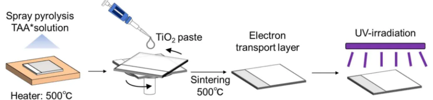
Then, the ETLs were prepared on the TCO substrates as shown in Fig. 2.4. The substrates were cleaned by ultrasonication in ethanol for 5 min and dried in air. The TiO2 compact layers were prepared by spray-pyrolysis
method; a solution of titanium diisopropoxide bis(acetylacetonate) (TAA, 75 wt% in isopropanol, Sigma-Aldrich) mixed with ethanol at the volume ratio of TAA:ethanol=2:25 was sprayed on the patterned substrates at 500°C. TiO2 mesoporous layers were then prepared by spin-coating a TiO2 paste (18NR-T, Dyesol), which
was diluted in ethanol at the weight ratio of 1:5, on the substrates at 4000 rpm for 25 s and annealed at 500°C for 30 min. The coated substrates were immerged in a 40 mM TiCl4 (99.0 %, Wako Pure Chemical Industry)
solution diluted in distilled water at 70°C for 30 min, followed by rinsing with ethanol and annealing at 500°C for 30 min.
Fig. 2.4 Schematic illustration of preparation processes of electron transport layer (ETL). Preparation of perovskite layer, hole transport layer (HTL) and metal electrodes
The perovskite layer and HTL were prepared in air with humidity of ~30%. The preparation processes are depicted in Fig. 2.5. The TiO2 coated substrates and 1 M PbI2 (>98.0 %, Tokyo Chemical Industry) solution
in N,Ndimethylformamide (DMF, 99.5 %, Nacalai tesque) were pre-heated at 60°C. Then, the PbI2 solution
was spin-coated on the substrates at 3000 rpm for 20 s (i.e. the 1st step). After annealing at 60°C for 10 min,
the substrates were dipped in a 10 mg/mL of CH3NH3I (MAI, 98 %, Wako Pure Chemical Industry) solution
dissolved in isopropanol for 20 s, followed by rinsing with isopropanol and annealing at 60°C for 10 min (i.e. the 2nd step). Then, 20 µL of MAI solution (20 mg/mL), CH
3NH3Br (MABr, 98 %, Wako Pure Chemical
Industry) solution (14 mg/mL) or mixed solution of MAI and MABr ((10 mg+7 mg)/mL) were dropped on the prepared MAPbI3 layers during the spinning at 4000 rpm for 35 s (i.e. the 3rd step).
The 3-step treated substrates were annealed at 60°C for 10 min, and then, the HTLs with the thickness of ~200 nm were prepared by spin-coating a spiro-MeOTAD solution. The spiro-MeOTAD solution in 1 mL chlorobenzene (99%, Nacalai tesque) was composed of 73 mg spiro-MeOTAD (99%, Sigma-Aldrich), 28.8 μL 4-tert-butylpyridine (TBP, 96.0%, Sigma-Aldrich) and 17 μL solution of [520 mg/mL lithium bis(trifluoromethylsulphonyl)imide salt (>98.0%, Tokyo Chemical Industry) in acetonitrile (99.5%, Wako Pure Chemical Industry)]. Finally, Ag electrodes with the thickness of ~50 nm were deposited on the HTLs with a thermal evaporator under 3×10⁻⁵ Torr. The completed solar cell is shown in Fig. 2.6.
25
Fig. 2.5 Schematic illustration of preparation processes for perovskite layer, hole transport layer (HTL), and metal electrodes.
Fig. 2.6 Appearance of the perovskite solar cell. The cell size is 12.5×12.5 mm2.
Herein after, CH3NH3Pb(I/Br)3 and CH3NH3(I/Br) will be denoted as MAPb(I/Br)3 and MA(I/Br),
respectively. As for the prepared samples, the relationship between the sample names and preparation conditions are summarized in Table 2.1.
Table 2.1 Relationship between sample names and preparation conditions in Chapter 2. Additional
spin-coating Without MAI solution
MA(I/Br) mixed
solution MABr solution Sample names 2-step only Additional MAI Additional MA(I,Br) Additional MABr
2.2.2 Characterizations X-ray diffraction (XRD)
Crystal structure and phases analysis of the prepared perovskite layers or completed cells were carried out by XRD (Multiflex, Cu-Kα, 40 kV and 40 mA, Rigaku). The sample was set so that the height of surface
matches that of sample holder (Fig. 2.7).
Fig. 2.7 Schematic illustration of sample set for XRD analysis. The perovskite layer on ETL or completed cell were used for the measurement.
26
Ultraviolet-visible absorption spectroscopy (UV-Vis)
Optical absorbance and transmittance spectra of the prepared perovskite layers on ETLs were measured by UV-Vis (UV-1280, Shimadzu). The light was irradiated from back TCO glass side (Fig. 2.8).
Fig. 2.8 Schematic illustration of UV-Vis. The light was irradiated from back TCO glass side. Bandgap estimation
To estimate bandgaps of the prepared perovskite layers, the absorbance spectra were converted to Tauc plots. The Tauc equation is expressed as following (eq. 2.1) [6],
(𝛼h𝜈)1/n= 𝐴(h𝜈 – 𝐸 ) (eq. 2.1)
where α is an absorption coefficient, h𝜈 is the photon energy (h is Planck constant, 𝜈 is frequency), A is a constant, and Eg is a bandgap gap. n takes “1/2” for a direct bandgap material and “2” for an in direct bandgap
material. Since MAPbI3 has the direct bandgap, n = 1/2 is used for MAPbI3. The αis expressed by the following
equation (eq. 2.2),
𝐼 = 𝐼 exp(−𝛼 × 𝑡)
In𝐼𝐼0 = 𝛼 × 𝑡 (eq. 2.2) where I is transmitted light intensity, I0 is incident light intensity, and t is thickness of the sample. Since the
absorbance (A) is expressed by following equation (eq. 2.3),
𝐴 = −𝑙𝑜𝑔 (𝐼𝐼
0) (eq. 2.3)
the α is calculated by following equation (eq. 2.4).
𝛼 = . × (eq. 2.4) Tauc plots for MAPbI3 is obtained by plotting (αℎ𝜈)2 for vertical axis and photon energy (h𝜈) for
horizontal axis. Then, a straight line is fitted to the liner part of the Tauc plots, and the bandgap is obtained from the photon energy at the intersection of the fitted straight line and background of the Tauc plots.
27
Scanning electron microscopy (SEM)
Surface and cross-section of the perovskite layers on ETLs were observed by SEM (JSM-5600LV, JEOL and SU-8020, Hitach High-technologies). For the cross-sectional observation, samples were broken into two pieces by making a notch with a diamond cutter, and the fracture surface was observed (Fig. 2.9).
Fig. 2.9 Schematic illustration of sample preparation for cross-sectional SEM observation. Current density-voltage (J-V) characterization
J-V characteristics were measured to evaluate photovoltaic performance with a DC voltage and current source/monitor (6241A, ADC Co.) and with a solar simulator (XES-40S1, SAN-EI Electric) which was calibrated to AM 1.5, 100 mW/cm2 with a standard silicon photodiode (BS-520BK, Bunkokeiki). The voltage
step and delay time were 20 mV and 50 ms, respectively. The voltage scan range was 0-1.1 V. The perovskite solar cells usually have a problem of hysteresis [7]; i.e. the different J-V characteristics are obtained depending on the voltage scan direction. Hence, the J-V characteristics were measured with both forward and back scans (forward scan: 0.0 → 1.1 V, back scan: 1.1 → 0.0 V). The active area was limited to 0.087 cm2 by using a
black mask.
There are two contact ways to the electrodes of perovskite solar cells as shown in Fig. 2.10. For the first method, the solar cell is turned over and it is placed on the metal pins for the contact. In this case, the light is irradiated from upper side. On the other hand, for the second method, the probes are touched from upper side and the light is irradiated from the bottom side. The first method was used in this thesis. Fig. 2.11 shows a laboratory-made sample stage for J-V measurement.
28
Fig. 2.11 Schematic illustration of the laboratory-made J-V measurement stage. Parameters obtained from the J-V measurement
By measuring the current with applied voltage, the J-V curve as shown in Fig. 2.12 is obtained. From the J-V curve, the J-V characteristics can be obtained, and those parameters are used for the evaluation of photovoltaic performance.
Fig. 2.12 J-V curve obtained from J-V measurement of solar cells. Short circuit current density: JSC (mA/cm2)
JSC is a current density obtained under the short circuit condition (applied voltage = 0), and it is the
maximum current obtained from the solar cell. A short circuit current (ISC) is generally measured in the actual
29
Open circuit voltage: VOC (V)
VOC is a voltage obtained under the open circuit condition (current = 0), and it is the maximum voltage
obtained from the solar cell. Fill factor: FF
FF is calculated by following equation, where the Jmax and Vmax are the current density and voltage at the
maximum power point, respectively.
FF = (Jmax × Vmax) / (JSC × VOC) (eq. 2.5)
Since the ideal maximum power obtained from the solar cell is calculated by JSC×VOC, the J-V curve
should be a square shape for the ideal solar cells. However, some resistance or leak current exists in the actual cell, and they decrease the generated power. Therefore, the actual power (Jmax× Vmax) is lower than the ideal
power. FF expresses a ratio of the actual power and the ideal power. When FF is closer to 1, the solar cell has smaller resistance and leak current, and the higher photovoltaic performance can be obtained.
Power conversion efficiency: PCE (%)
PCE is calculated by following equation (eq. 2.6). It expresses what percentage of the incident light energy is converted to electricity by the solar cell.
PCE (%) = Generated power (mW) / Incident light intensity (mW)×100 = (Jmax (mA/cm2) × Vmax (V)) / 100 (mW/cm2) × 100
= VOC × JSC × FF (eq. 2.6)
The incident light intensity is generally calibrated to AM 1.5, 100 mW/cm2 to measure the photovoltaic
performance under the fixed condition. Air mass (AM) represents an optical path length of the sun light through atmosphere of the Earth. The spectrum of sun light is different before and after traveling through the atmosphere, since the atmosphere partially absorbs or scatters the sun light. The spectrum of the sun light which enters vertically against the sea level is AM 1, and the AM 1.5 corresponds to the spectrum of solar zenith angle of ~48.2° (Fig. 2.13). The AM 1.5, light intensity of 100 mW/cm2, and measurement temperature
of 25°C are used as Standard Test Cell conditions.
30
2.3 Results and Discussion
2.3.1 Phase and crystal structure analysis of perovskite layer
Figure 2.14 shows XRD patterns of the prepared perovskite solar cells in the range of 2θ = 10-70° and enlarged ones at 2θ = 27.5-29.0°. For the 2-step only sample, relatively strong peaks at ~12.6°, ~14.5°, ~28.3°, and ~35.2° were confirmed. The peaks at ~14.5°, ~28.3°, and ~35.2° correspond to 110, 220, and 312 peaks of tetragonal MAPbI3 [8], indicating that MAPbI3 was synthesized from the reaction of PbI2 and MAI. However,
since the peak at ~12.6° corresponding to 001 peak of PbI2 [9]was also conformed, the unreacted PbI2 remained
in the 2-step prepared perovskite layer. After the additional spin-coating (the 3rd step), the intensity of PbI 2
peak significantly decreased and those for perovskite increased. This result indicates that the unreacted PbI2
was converted into perovskite phase by the additional spin-coating. Although the 3-step prepared perovskite layers still had small amount of unreacted PbI2, it may be converted into perovskite phase by controlling the
concentration or contact time of the additional spin-coating solution.
As for the zoomed range at 27.5-29.0°, the peaks at ~28.0° and ~28.3° corresponding to the 004 and 220 peaks of tetragonal MAPbI3 [8] were confirmed for the additionally MAI spin-coated perovskite layer. The 004
peak was not clearly confirmed in the 2-step only sample possibly due to the smaller peak intensity than that for additionally MAI spin-coated sample. With the additional spin-coating of the MA(I,Br) and MABr solution, the 220 peaks were shifted to larger angle and intensities of 004 peaks became smaller. The peak shift to large angle and the disappearance of the peak split indicate the shrinkage of lattice constants and the phase change from tetragonal phase to cubic phase. Since the ionic radius of Br- is smaller than that of I- and the MAPbBr
3
has cubic phase at the room temperature as mentioned in Chapter 1, these results suggest that the formation of MAPbI3−xBrx by the substitution of I- with Br- [10,11].
Fig. 2.14 XRD patters of the prepared perovskite layers on ETLs with and without additional MA(I/Br) spin-coating.
31
Then, the amount of unreacted PbI2 converted into perovskite by the additional spin-coating was estimated
from the integrated intensity of the PbI2 peak at ~12.6° (001 reflection). Figure 2.15shows XRD patterns of a
PbI2 layer (1st step, before dipping in MAI), 2-step prepared MAPbI3, and additionally MAI spin-coated
perovskite layers at 11-15°. The integrated intensities of the PbI2 peaks (001 reflection) and MAPbI3 peaks
(110 reflection) estimated from the XRD data are summarized in Table 2.2. The integrated intensity of the PbI2
peak decreased to ~20% of the original value after the dipping in MAI solution (2nd step). This suggests that
~80% of PbI2 was converted into MAPbI3 and ~20% of PbI2 still remains as the unreacted PbI2 in the 2-step
prepared perovskite layer. After the additional MAI spin-coating (3rd step), the integrated intensity of PbI 2
further decreased to ~5% of the original value, which indicates that the additional spin-coating further converted ~15% of unreacted PbI2 into perovskite.
The increase of integrated intensity for MAPbI3 peak by the conversion of 1% PbI2 is calculated to be
~96.8 cps·deg (7779/80.4). From this estimation, the conversion of 15% of PbI2 by the additional spin-coating
will increase the integrated intensity of MAPbI3 peak by ~1440 cps·deg (96.8×14.9). Therefore, the expected
integral intensity of MAPbI3 peak after the additional MAI spin-coating is ~9220 cps·deg (7779+1440).
Actually, the integrated intensity of the MAPbI3 peak obtained from the XRD data was ~9300 cps·deg, which
is in good agreement with the expected value. This result suggests a proportional relationship between the decrease of integrated intensity for PbI2: 001 peak and increase of MAPbI3: 110 peak. It supports an accuracy
of the estimation for decreased amount of PbI2.
Fig. 2.15 XRD patterns of a PbI2 layer (1st step, before dipping in MAI), 2-step prepared MAPbI3 (2nd step),
and additionally MAI spin-coated perovskite layers (3rd step) at 11-15°.
32
2.3.2 Optical property analysis and bandgap estimation of perovskite layer
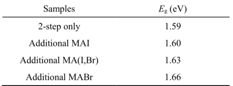
Figure 2.16 shows absorbance spectra of the prepared perovskite layers on ETLs in the range of 600-800 nm. The Tauc plots converted from the absorbance spectra are shown in Fig. 2.17, and the estimated bandgaps are summarized in Table 2.3. The 2-step prepared sample showed an absorption edge at ~780 nm, and the bandgap was estimated to be ~1.59 eV. This is comparable value with some reported bandgaps of MAPbI3
[12,13]. The absorption edge of the additionally MAI spin-coated sample also existed at ~780 nm and the bandgap value was ~1.60 eV, which was similar to that of 2-step prepared sample. Since the bandgaps were comparable between 2-step prepared sample and additionally MAI spin-coated sample, the additional MAI spin-coating converted the unreacted PbI2 into MAPbI3 without obvious effects on the composition. On the
other hand, blue-shifts of absorption edges and increases of bandgaps were confirmed for the additionally MA(I,Br) and MABr spin-coated samples. The bandgaps of additional MA(I,Br) and MABr were estimated to be 1.63 eV and 1.66 eV, respectively. Since the bandgap of MAPbBr3 is larger than that of MAPbI3 [14,15],
these results also indicate the conversion of MAPbI3 into MAPbI3−xBrx by the substitution of I- with Br-.
Fig. 2.16 Absorbance spectra of the prepared perovskite layers.