Characterization of the chemical bonding at
the interfaces of SiO?-related materials using
microscopic infrared spectroscopy and
attenuated total reflection
著者(英)
Hirofumi Seki
学位名
博士 (工学)
学位授与機関
関西学院大学
学位授与番号
34504乙第378号
Characterization of the chemical bonding at the interfaces of
SiO
2-related materials using microscopic infrared spectroscopy
and attenuated total reflection
A Thesis for the Degree
of
Doctor of Engineering
Submitted to
School of Science and Technology
Kwansei-Gakuin University
By
Hirofumi Seki
i
CONTENTS
General introduction 1
Motivation and background to the research 2
Previous research and adaptation of FT-IR analysis for semiconductor materials 4
Novelty and originality of this research 6
Outline of this study 7
References 9
Chapter.1: Characterization of Ashing Damage in Depth Direction in Low-k Dielectric Films by Microscopic IR Method 1 9 Abstract 20
Introduction 21
Experimental detail 22
Result and discussion 23
Conclusion 26
References 27
Chapter.2: Characterization of process-induced damage in Cu/low-k interconnect structure by microscopic infrared spectroscopy with polarized infrared light 36
Abstract 37
Introduction 38
Experimental detail 40
Result and discussion 42
Conclusion 46
References 48
Chapter.3: Characterization of Inhomogeneity in SiO2 Films on 4H-SiC Epitaxial Substrate by a Combination of Fourier Transform Infrared and Cathodoluminescence Spectroscopy 63
Abstract 64
Introduction 65
Experimental detail 68
ii
Conclusion 75
References 76
Chapter.4: Characterization of Thermal Oxides on 4H-SiC Epitaxial Substrates Using Fourier-Transform Infrared Spectroscopy 86
Abstract 87
Introduction 88
Experimental detail 90
Result and discussion 92
Conclusion 98
References 100
List of publications 112
Acknowledgement 115
iii
Abbreviations
AES: Auger Electron Spectroscopy AFM: Atomic Force Microscopy ATR: Attenuated Total Reflection
ASTM: American Society for Testing and Materials CCD: Charge Coupled Device
CL: Cathodoluminescence CM: Channel Mobility
CMP: Chemical Mechanical Polishing CVD: Chemical Vapor Deposition Dit: Interface trap density
EDX: Energy Dispersive X-ray analysis EELS: Electron Energy-Loss Spectroscopy EPMA: Electron Probe Microanalyzer ESR: Electron Spin Resonance
HFS: Hydrogen Forward Scattering
FT-IR: Fourier Transform Infrared Spectroscopy GSP: Gradient Shaving Preparation
ICP-MS: Inductively Coupled Plasma Mass Spectrometer ISSG: In-Situ Steam Generation
MOSFET: Metal-Oxide Semiconductor Field-Effect Transistor MSQ: Methyl Silsequioxane
NBOHC: Non-Bridging Oxidation Hole Center NMR: Nuclear Magnetic Resonance analysis OVC: Oxygen Vacancy Center
PALS: Positron Annihilation Lifetime Spectroscopy POA: Post Oxidation Annealing
PL: Photoluminescence
Qeff: Effective fixed charge density
Raman: Raman scattering spectroscopy
RBS: Rutherford Back Scattering Spectrometry RTO: Rapid Thermal Oxidation
iv
SEM: Scanning Electron Microscopy
SEMI: Semiconductor Equipment and Materials International SIMS: Secondary Ion Mass Spectroscopy
SPP: Surface Phonon Polariton SR: Spreading Resistance
SSRM: Scanning Spreading Resistance Microscopy STM: Scanning Tunneling Microscopy
ULSI: Ultra Large Scale Integration TEM: Transmission Electron Microscopy TO: Transverse Optic
TOF-SIMS: Time-of-Flight Secondary Ion Mass Spectrometry XPS: X-ray Photoelectron Spectroscopy
XRD: X-ray Diffractometry XRF: X-ray Fluorescence analysis XRR: X-ray Reflectometry
- 1 -
- 2 -
Motivation and background to this research
Semiconductors, as exemplified by ultra large scale integration (ULSI) devices, currently feature high-density integration as a result of the miniaturization of their design. They have conformed to Moore's Law in that the number of transistors in a dense integrated circuit has doubled approximately every two years.1) The size of the gate electrodes of semiconductors was originally on the micrometer level, but has gradually become smaller and now is typically less than 100 nm. Manufacturing based on a design rule of the several nm level has been the subject of considerable study such that it is gradually being commercialized. To miniaturize semiconductor devices, different materials, each offering their own unique advantages, have been adopted. For example, wiring was originally fabricated using aluminum, while copper is commonly used now. Meanwhile, the interlayer insulator material between the wiring layers has changed from silicon dioxide (SiO2) to a low dielectric value
material (Low-k material) that incorporates organic components. Gate insulator films, which were originally silicon dioxide (SiO2), are now formed using high-k films such as hafnium
oxide or hafnium silicate.2, 3)
As manufacturing design rules approach the nm level, the miniaturization of transistors is approaching its limit. In recent years, some aggressive research addressing the improvement of devices has considered 3-dimensional integration or has introduced new materials. Multi-functionality has been achieved by adding sensors, detectors, and so on. 2) On the other hand, in the area of semiconductor substrates, the use of Si has been proposed, but Ge substrates and next-generation materials of the III-V groups are also being studied. Silicon carbide (SiC) substrates are already being used in power devices instead of a Si substrate. The use of a gallium nitride (GaN) substrate has also been the subject of various studies.4-6)
Semiconductor devices, such as those used in smartphones, are indispensable to our daily lives. In addition, automotive applications of semiconductors, such as for sensors, have expanded, with quality and reliability demands becoming more severe. Given that semiconductor devices have multilayer structures incorporating different materials, the manufacturing process has become extremely complicated, and the processing technology has become clearly divided into very wide segments. In addition, as materials become thinner, the surface and interface properties of thin films are important in that they have a critical effect on the device performance. For this reason, it is extremely important to have a method in place for evaluating ultra-thin films or very small regions, and to identify the physical
- 3 -
parameters that affect the electrical characteristics while developing the manufacturing process. Therefore, analytical techniques are indispensable to semiconductor process development in that they provide a means of searching for and evaluating such physical parameters.
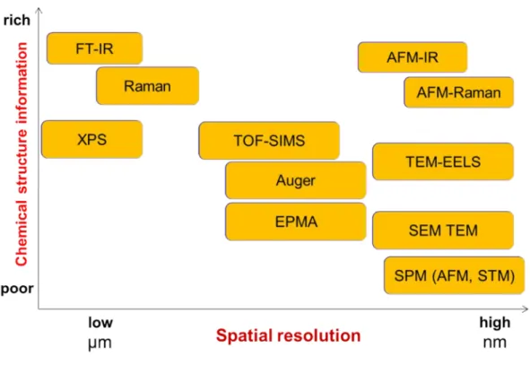
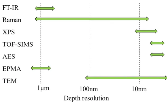
Analytical techniques for semiconductors are summarized in Table 1-1. The main techniques for analyzing semiconductors are transmission electron microscope (TEM) observations to confirm the actual nm-level device structure, secondary ion mass spectrometer (SIMS) analysis to confirm the depth profile of impurities that affect the electrical property, and inductively coupled plasma mass spectrometer (ICP-MS) analysis to quantify the trace impurities. These techniques are widely used and are well-established analytical techniques. Meanwhile, in spectroscopic analysis methods such as Fourier transform infrared (FT-IR) and Raman spectroscopy, characteristic information such as the chemical bonding state information is obtained by spectroscopic methods, providing information which cannot be obtained by other means. However, there are several problems related to the analysis of the ultra-thin films found in semiconductor devices. One is that the analysis is very difficult because spectral data are obtained by the measurements and spectral analysis requires considerable experience and knowledge. Fig. 1-1 shows the spatial resolution and the amount of chemical structure information produced by the analytical techniques applied to semiconductors. The unit size of semiconductor devices is nowadays approaching the nm scale due to the miniaturization described above, consequently requiring the ability to conduct analyses of a very small area. As can be seen from the figure, spectroscopic methods such as FT-IR and Raman spectroscopy provide rich information about the chemical structure, but the spatial resolution is in the order of microns, making it difficult to directly apply these to the analysis of semiconductor devices. Fig. 1-2 compares the depth resolution for each analysis method. FT-IR has a depth resolution of the submicron to micron order, whereas other surface analysis methods have a resolution on the order of nanometers, making them unsuitable for application to the analysis of ultra-thin films with a smaller thickness. However, FT-IR has been used as an effective means of analyzing SiO2 films for a long time, and is
well covered by the literature.7-22) It is expected that it will be possible to obtain useful information by adapting FT-IR to the evaluation of semiconductor devices.
Therefore, this study sets out to establish a tool for evaluating the process development of a semiconductor device by using FT-IR analysis. The author considered analytical methods for evaluating the depth direction and interfaces of thin films, based on FT-IR. The author
- 4 -
overcame the problems of low spatial resolution and low depth resolution that characterize FT-IR analysis by improving the pretreatment and measurement methods while attempting to establish a method for evaluating semiconductor materials, especially the manufacturing process development of SiO2 materials for which FT-IR has already successfully produced
results. In particular, the author examined the methods used to evaluate the depth direction and interfaces of SiO2 materials (especially low-k films and SiO2 films formed on a SiC
substrate) and compared the physical parameters obtained by these methods with the electrical properties. Finally, the author evaluated the effectiveness of each of the methods.
Previous research and adaptation of FT-IR analysis to semiconductor materials
FT-IR analysis of semiconductor materials
FT-IR is also widely utilized for inorganic materials such as semiconductors.23) For example, it is generally used for quantitative analyses of oxygen, carbon, and nitrogen in silicon and for determining the amounts of dopants (boron, phosphate, gallium, aluminum, etc.) at low temperatures (around 10 K). The technique is covered by international standards such as the SEMI International Standards and the ASTM standards.24) FT-IR is used to detecting the constituent gases in emissions and the gas concentrations in manufacturing chambers.25) FT-IR is often applied to the quantitative analysis of functional groups (the N-H and Si-H groups in silicon nitride film and the Si-H groups in amorphous silicon) in the areas of semiconductors and solar cells.26-29) It is useful for characterizing the photo reaction of resists and the degradation of organic materials such as resins or films.
Compared to other analytical techniques, FT-IR has some unique features in that it can be used to detect hydrogen-related bonds such as Si-H and C-H groups and moisture-related OH and metal-OH bonds. It provides a comparatively simple means of investigating the chemical bonding structure of a material.
Depth analysis of thin film by FT-IR method
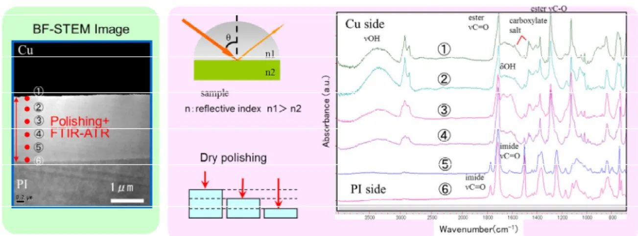
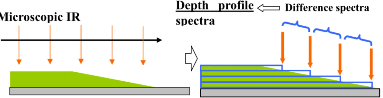
The conventional methods of analyzing the depth direction of organic thin films are shown in Fig. 1-3. Evaluation-based methods include those in which cross-sectional processing is carried out and in which measurement is performed from the sectional direction shown in Fig. 1-3(a), while the FT-IR measurement is repeated while slowly removing material by means of mechanical polishing or ion milling, as shown in Fig. 1-3(b), (c). An example of depth
- 5 -
analysis is shown in Fig. 1-4. The chemical bonding state in the depth direction was evaluated in the depth direction, with a sub-micron resolution, by repeating the attenuated total reflection (ATR) method and the mechanical polishing for the adhesive layer at the polyimide film/copper thin film interface. The depth profile spectra were obtained at each measuring point. It is assumed that the amounts of carboxylate salt and OH groups increased. Therefore, the hydroxylation of the ester groups occurred. A depth analysis can be carried by repeating the mechanical polishing and ATR measurements for a thin film. However, it is difficult to carry out a depth direction analysis for submicron organic thin films when using mechanical polishing. In addition, in the case of ion milling, the organic film is damaged. While it is possible to discuss the depth distribution of the elemental information, it is difficult to argue the original chemical bonding state due to the deterioration of the organic film. Therefore, there is a need for a method of evaluating the chemical bonding state in submicron organic thin films. The author developed a new means of evaluating the state of chemical bonding in submicron organic thin films by introducing a new pretreatment method. Use of FT-IR to evaluate damage in low-k films in device structure
A cross-sectional TEM photograph and a schematic view of the multilayer interconnection structure of a commercial LSI device are shown in Fig. 1-5. The semiconductor device has a structure in which different materials are stacked three-dimensionally. Low-k materials can be applied as dielectric interlayers to replace the SiO2 dielectric layer.5) Low-k materials
basically consist of Si-O frameworks and Si-CH3, Si-H terminal groups. Therefore, they
incorporate many pores into the film to reduce the dielectric constant. However, low-k films have organic components and therefore tend to exhibit changes in their structure owing to plasma processes such as etching, ashing, and metal deposition. The structural changes in low-k films increase the dielectric constant and degrade the hygroscopic property. Therefore, it is necessary to investigate the process-induced damage to low-k films. Regarding there being no patterning of low-k films, there have been many studies using FT-IR.30-33) However, as the thickness of a low-k film is of the submicron level, there have been no reports of evaluations of the chemical bond state of low-k films in the depth direction.
The TEM image shows how a low-k film is used as an interlayer insulating film, filling the spaces between the Cu wiring layers.In fact, it is important to evaluate the damage to the side walls and bottom of low-k films during trench formation processes. Although damage evaluations have been conducted by means of electron energy-loss spectroscopy
- 6 -
(TEM-EELS) or TEM observations after HF treatment, there have been very few reports of FT-IR evaluations of samples with such a trench structure.
Characterization of silicon dioxide by FT-IR analysis
SiO2 films are remarkable and useful materials in the semiconductor industry. They exhibit
good insulation properties and a uniform thickness. SiO2 can dissolve in a HF acid solution,
whereas Si substrates do not dissolve. A thin oxide film can thus be easily prepared by the oxidation of the Si substrate. Therefore, these properties enable the fabrication of metal oxide semiconductor field-effect transistors (MOSFET), which are a type of transistor used for amplifying or switching electronic signals. However, defects and impurities arise in a SiO2
film, and it is difficult to control the properties of these films, as shown in Fig. 1-6. Many reports have focused on the characterization and improvement of SiO2 films. 7-22) As the
thickness and width of the film are made smaller, it is important to control the interfacial structures at the interface between the oxide and the substrate. Many researchers have investigated and improved these properties. In our group, a special wet pretreatment process was developed to form an incline on an ultra-thin SiO2 film. It was found, using FT-IR, that
the amount of Si-O peak shift at the SiO2/Si interface is closely correlated to the leakage
current, as shown in Fig.1-7.9) In recent years, SiC substrates have been used for power devices.6) However, there are several longstanding problems related to the high trap densities and the high fixed-charge density at the SiO2/SiC interface; these high values can degrade the
channel mobility of SiC MOSFETs. These problems are believed to be caused by poor interfacial properties. Therefore, the interfacial chemical bonding structure should be investigated by FT-IR analysis. However, although a few studies have used FT-IR analysis to investigate the application of SiO2 films to SiC substrates, none have discussed the
relationship between the chemical bonding structure and the electrical properties.
Novelty and originality of this study
In this study, the author developed a method for evaluating the ultra-thin films used in semiconductor devices.
The completely new depth direction analysis method can evaluate the chemical bonding state at depth intervals of several tens of nm. This can be applied not only to a low-k film but also to an ultra-thin film of sub-micron thickness, including the organic components that easily
- 7 -
degrade. In addition, the method enables depth direction analysis by applying not only FT-IR analysis but also other surface analysis methods to the inclined surface created by the newly introduced pretreatment method.
The author also developed a method for evaluating a trench structure sample with a Cu/low-k line and space structure. Previously, FT-IR had not been applied to non-patterned films, and therefore had not been used to evaluate a trench structure like that of a real device. By improving the sample structure and measurement method, the author was able to perform an evaluation of a trench structure by using FT-IR. This is a useful method that can be applied to the development of other semiconductor devices having a trench structure, such as dynamic random access memory (DRAM) and NAND flash memory.
The author characterized the chemical bonding structure at the SiO2/SiC substrate interface
by combining wet etching and the ATR method. Thus, a physical parameter that is related to the electrical properties was identified for the first time.
Outline of this study
This thesis is composed of four chapters and a preface. Each chapter is outlined below: In the current chapter, the author describes the purpose of the research, previous research, the adaptation of FT-IR to semiconductor materials, and the novelty and originality of this research.
In Chapter 1, the author reports on the development of a useful pretreatment method (referred to as gradient shaving preparation (GSP)) to investigate the chemical bonding structure of sub-micron thickness thin films in the depth direction by using FT-IR measurements. The author investigates the chemical structure changes in the depth direction of low-k dielectric films, 250-nm thick, after several ashing processes, by using the microscopic FT-IR method, and characterizes the type and extent of the ashing damage in the low-k films. The author confirms that this pretreatment method is useful for characterizing the chemical bonding of thin organic film in the depth direction.
In Chapter 2, the author sets out to evaluate the process-induced damage for a Cu/low-k interconnect structure using polarized IR light for different widths of low-k spaces and Cu lines, and for different heights of Cu lines, on Si substrates. Although the width of both the Cu line and the low-k space is 70 nm, considerably smaller than the wavelength of IR light, FT-IR spectra of the low-k film were obtained for the Cu/low-k interconnect structure. A
- 8 -
suitable method was established for measuring the process-induced damage on the sidewalls of the low-k films that was not detected by TEM-EELS using microscopic IR polarized light. In Chapter 3, the author presents the measured FT-IR and cathodoluminescence (CL) spectra of SiO2 films grown on 4H-SiC substrates, confirming that the phonon observes the upper
branch of the surface phonon polaritons (SPPs) in the SiO2 films and that its frequency is
sensitive to the oxide thickness. The relative intensity of the upper branch of SPPs normalized by that of the transverse optical phonon (TO) tended to increase as the channel mobility (CM) decreased. A comparison between the FT-IR and CL measurements shows that the relative intensity is correlated to the inhomogeneity in the SiO2/SiC interface, and the
CM of SiC devices.
In Chapter 4, the author presents the measured FT-IR spectra of thermal oxides with different electrical properties grown on 4H-SiC substrates and discusses the interfacial bonding structure and stresses in the depth direction as determined with repeated ATR measurements and wet etching. For the thinner thermal oxides (SiO2 thicknesses of less than 3 nm), the peak
frequency of the TO mode of the oxides on the 4H-SiC substrate is red-shifted as the oxide layer thickness decreases. The channel mobilities are correlated with the degree of the shift of the TO mode in samples with an oxide thickness of less than 3 nm. It appears that the compressive stress at the SiO2/SiC interface generates silicon suboxide components and
weakens the Si-O bonds. Therefore, the TO mode was red-shifted and the oxygen deficiency increased to relax the compressive stress in the oxide with < 3 nm thickness.
- 9 -
REFERENCES
1G.E. Moore,”Cramming more components onto integrated circuits,” Electronics, 38,
114(1965).
2International Technology roadmap for Semiconductors (ITRS) 2008.www.itrs.net. 3J. Robertson, Solid-State Electron. 49, 283 (2005).
4V. Tilak, B. Green, V. Kaper, H. Kim, T. Prunty, J. Smart, et al., IEEE Electron Dev Lett. 22,
504 (2001).
5R.D. Goldblatt, B. Agarwala, M.B. Anand, E.P. Barth, G.A. Biery, Z.G. Chen, and S. Gohen,
Proc. of IITC. 1, 261 (2000).
6J.A. Cooper, Jr, Phys. Stat. Sol. (a), 162(1), 305 (1997).
7C. Martinet and R.A.B. Devine, J. Appl. Phys. 77, 4343 (1995).
8K.T. Queeney, M.K. Weldon, J.P. Chang, Y.J. Chabal, A.B. Gurevich, J. Sapjeta, and R.L.
Opila, J. Appl. Phys. 87, 1322 (2000).
9N. Nagai, K. Terada, Y. Muraji, H. Hashimoto, T. Maeda, Y. Maeda, E. Tahara, N. Tokai, and
A. Hatta, J. Appl. Phys. 91, 4747 (2002).
10K. Kim, J. Song, D. Kwon, and G.S. Lee, Appl. Phys. Lett. 72, 1247–1249 (1998). 11I. Boyd and J. Wilson, Appl. Phys. Lett. 50, 320 (1987).
12M.L. Green, E.P. Gusev, R. Degraeve, and E.L. Garfunkel, J. Appl. Phys. 90, 2057 (2001). 13N. Hirashita, S. Tokitoh, and H. Uchida, Jpn. J. Appl. Phys. 32, 1787 (1993).
14J. Shiuh, Si-chen Lee, J. Appl. Phys. 77, 1805 (1995).
15T. Yamaguchi and N. Sakamoto, J. Appl. Phys. 83, 554 (1998). 16Y. Kim, M. Hwang, and H. Kim, J. Appl. Phys. 90, 3367 (2001).
17R. Nonogaki, S. Nakai, S. Yamada, and T. Wada, J. Vac. Sci. Technol. A. 16, 2827 (1998). 18P.G. Pai, S.S. Chao, Y. Takagi, and G. Locovsky, J. Vac. Sci. Technol. A. 4, 689 (1986). 19J.T. Fitch, G. Lucovsky, E. Kobeda, and E.A. Irene, J. Vac. Sci. Technol. B. 7, 153 (1989). 20G. Lucovsky, M.J. Manitini, J.K. Srivastava, and E.A. Irena, J. Vac. Sci. Technol. B5, 530
- 10 -
(1987).
21W.A. Pliskin and H.S. Lehman, J. Electrochem. Soc. 112, 1013 (1965).
22S. Miyazaki, H. Nishimura, M. Fukuda, L. Ley, and J. Ristein, Appl. Surf. Sci. 113/114. 585
(1997).
23M. Tasumi, Introduction to Experimental Infrared Spectroscopy, John Wiley & Sons,
(2015).
24ASTM Designation F1188 – Test Method for Interstitial Atomic Oxygen Content of Silicon
by Infrared Absorption, F1391 – Test Method for Substitutional Atomic Carbon Content by Infrared Absorption.
25R. Jaaniso and O.K. Ta, Semiconductor Gas Sensors, Woodhead Publishing Limited,
(2013).
26W.A. Lanford and M. J. Rand, J. Appl. Phys. 49, 2473 (1978).
27G. Sasaki, M. Kondo, S. Fujita and A. Sasaki, Jpn. J. Appl. Phys. 21, 1394 (1982). 28G. Lucovsky, Solid State Commun. 29, 571 (1979).
29M.H. Brodsky et al., Phys. Rev. B16, 3556 (1977). 30A. Grill, J. Appl. Phys. 93, 1785 (2003).
31A. Grill and D.A. Neumayer, J. Appl. Phys. 94, 6697 (2003).
32B. Zhao and M. Brongo, Mater. Res. Soc. Symp. Proc. 565, 137 (1999).
33J.-N. Sun, D.W. Gidley, T.L. Dull, W.E. Frieze, A.F. Yee, E.T. Ryan, S. Lin, and J. Wetzel, J.
- 11 -
Table. 1-1 Analysis methods for semiconductor devices.
Information Analytical methods
Composition SIMS, EPMA,TEM-EDX, EELS, AES, RBS, XRF, XPS Chemical structure FT-IR, XPS, NMR, Raman, TEM-EELS, AES
Morphology TEM, SEM, AFM
Defect/crystallinity TEM, CL, PL, Raman, XRD, ESR, FT-IR Carrier concentration SCM, SSRM, SR
Stress/strain Raman, XRD, TEM
Roughness AFM, STM, TEM, SEM, XRR Voids TEM, SEM, PALS
Thickness/density Ellipsometry, XRR, RBS Impurity profile SIMS
- 12 -
- 13 -
- 14 -
- 15 -
- 16 -
Fig. 1-5. (a) TEM cross section image of commercial device. (b) Schematic view of trench formation process.
- 17 -
- 18 -
Fig. 1-7. (a) Depth profile spectra for 9-nm SiO2 film which exhibited different electrical properties. (b) Si–O peak positions as a function of SiO2 thickness
- 19 -
Chapter 1
Characterization of Ashing Damage in Depth in Low-k Dielectric Films by Microscopic IR Method
- 20 -
ABSTRACT
The author developed special pretreatment for the depth analysis and investigated the ashing damages of low-k films in the depth direction by the gradient shaving preparation (GSP) using the microscopic IR method. Ashing processes were performed on the MSQ films on Si substrates under conditions in which a fixed amount of resist was removed using O2,
NH3, and He/H2 gases. The Si-CH3 bond decreased from only the surface area to a depth of
approximately 100 nm in the NH3 ashing, whereas, in the O2 ashing, there is an extremely
low level of concentration over the entire depth. Further, a change in the structure of the Si-O network occurred. On the other hand, in the He/H2 ashing, no change in the film structure
was observed. Microscopic FT-IR with GSP is useful technique to characterize chemical structure in depth direction for thin low-k film.
- 21 -
INTRODUCTION
Advanced ultra-large-scale integration (ULSI) requires the replacement of a SiO2 (k = 4.1)
dielectric interlayer material with one that has a lower dielectric constant, in order to prevent signal delay. Low-k films have recently been used as interlayer dielectric materials for advanced Cu/low-k interconnects1-5. MSQ (methyl silsequioxane) is one possible low-k material for use as a replacement. However, MSQ is more susceptible to changes in its structure by treatments such as dry etching or ashing processes compared to more conventional SiO2 materials. Treatment via one of these processes induces an increase in the
dielectric constant and/or degradation with regard to the hygroscopic properties. Therefore, it is important to gain knowledge about the quality and origin of the process-induced damage and the depth of the damage to improve these manufacturing processes. Fourier transform infrared (FT-IR) analysis easily reveals the chemical bonding structure of porous low-k films in a quantitative manner, and it does not affect the film properties during spectral measurements;2,3 as such, FT-IR has been used in previous studies on low-k films.5-15 Furthermore, FT-IR is an effective tool for characterizing a blanket low-k film processed via various plasma treatments. However, it is difficult to evaluate the depth of a chemical bonding structure in sub-micron thickness low-k thin films, and structural changes in the depth direction have not yet been reported. Here, we have developed a new pretreatment method for evaluating chemical bonding in the depth direction for such thin films, and evaluated the chemical structural changes in this direction in low-k dielectric films after several ashing processes using a GSP method with microscopic IR techniques.
- 22 -
EXPERIMENTAL DETAIL
250-nm thick porous MSQ films (k = 2.3) were prepared on Si (100) substrates, and subsequently, the ashing processes were performed on the MSQ films under conditions in which a fixed amount of resist was removed using O2, NH3, and He/H2 gases. A Si substrate
with more than 1 Ωcm resistivity was used in this study. IR light passes through this substrate, and therefore, transmittance measurements can be carried out. The ashing damage to the MSQ films was characterized by Fourier transform infrared spectroscopy (FT-IR), X-ray photoelectron spectroscopy (XPS), Rutherford back scattering/Hydrogen forward scattering spectrometry (RBS/HFS), and Raman spectroscopy techniques. Obtained information for each analysis was shown in Table 2-1. The FT-IR measurement in depth was performed by line-scanned transmittance measurements for the slope processed by the gradient shaving preparation (GSP) using the microscopic IR method, as shown in figure 2-1 16.
GSP is a mechanical pretreatment method that does not use water and/or solution, or argon ions etc. Therefore, the low-k film does not suffer the damages under this pretreatment process. The slope obtained by GSP is more than 1000 times that of the thickness of low-k films. Information on the depth direction of the film can be obtained by some line-scanned surface analytical techniques. The information regarding a certain depth is acquired when the IR beam is used as an analytical probe from the obtained difference in adjacent measurement positions. Therefore, depth profile spectra were obtained by the subtraction of each raw spectrum from the next one.
- 23 -
RESULTS AND DISCUSSION
Changes in the dielectric constant by ashing
The dielectric constants of low-k films were measured by the mercury probe. Obtained dielectric constant of MSQ films were shown in table 2-2. No change in the dielectric constant by the He/H2 ashing was observed. On the other hand, by the O2 and NH3 ashing, an
increase was observed in the dielectric constant by approximately 42.6% and 13.9%, respectively 17. In the view of electrical property, O2 and NH3 ashing cause process induced
damage for low-k film and He/H2 ashing cause no damage for low-k film.
Change of chemical structure in depth by ashing
Figure 2-2 shows the IR transmission spectra of the MSQ films. The Si-CH3 band appeared
at 1260 cm-1 and decreased in the NH3 and O2 ashing.3 The degree of change is relatively
minor in NH3 ashing as compared to O2 ashing. Furthermore, the Si-OH band appeared
around 950 cm-1, which indicated that the MSQ film might tend to absorb moisture in the NH3 and O2 ashing. The Si-H band appeared at 900 cm-1 and increased in the NH3 and He/H2
ashing. It is presumed that the terminal functional groups of the Si-O network changed by ashing. In case of He/N2 ashing, there is no damage in electrical property. However, Si-H
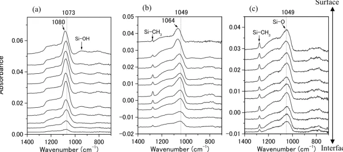
groups increased by the ashing. Si-H groups might not have any effect for electrical property. Figure 2-3 shows the depth profile spectra obtained by the microscopic IR measurements. The upper spectra in each figure are those of the surface, and the lower spectra are those of the interface in the MSQ film. Each spectrum contained information pertaining to the MSQ films for a depth of 25 nm. In the reference sample (c), no change in the spectrum was observed in the depth direction. However, in the case of O2 (a) and NH3 (b) ashing, changes
- 24 -
NH3 ashing showed a shape similar to that of the reference. On the other hand, it was found
that a peak position for the Si-O stretching mode appeared around 1049 cm-1 near at the interface and was shifted to a small extent to 1064 cm-1 at the surface area. This implies that the structure of a Si-O network, which is the primary network in the MSQ film, changes near the surface by the NH3 ashing.
In the O2 ashing, the peak position for the Si-O stretching around 1073 cm-1 at the interface
was shifted to a small extent to 1080 cm-1 near the surface area. The Si-O peak positions were blue-shifted compared with NH3 ashing and reference. The Si-O peak position of low-k films
tends to blue-shift due to Si-O network cross linkage progressing. It is presumed that the MSQ film transformed into a SiO2 likestructure in entire film in O2 ashing and on the surface
of low-k film in NH3 ashing.
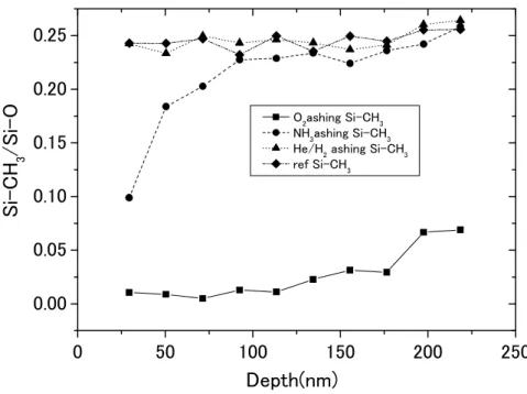
Figure 2-4 shows the depth profile of the ratios of the peak intensity of the 1260 cm-1 Si-CH3
band to the peak intensity of the Si-O band. It indicated that the Si-CH3 bond decreased from
only the surface region to a depth of approximately 100 nm in the NH3 ashing, whereas, in
the O2 ashing, there is an extremely low level of concentration over the entire depth. On the
other hand, no change in the amount of Si-CH3 in the depth direction was observed in the
He/H2 ashing.
Changes in the composition of MSQ films by ashing
Tables 2-3 and 2-4 show the composition of MSQ films characterized by the RBS/HFS and XPS. RBS/HFS gave the composition of MSQ films as a bulk property, whereas XPS gave the composition at the surface of MSQ films. The decrease in the amount of carbon and hydrogen and the increase in the amount of oxygen in the MSQ film in the O2 and NH3
ashing can be observed. Nitrogen existed in the surface of the MSQ film in the NH3 ashing.
- 25 -
Changes in the Si-O network of MSQ films by ashing
Figure 2-5 shows the Raman spectra of the MSQ films. The Peaks were assigned a 4-fold ring structure of the Si-O and/or random network of the SiO2 at 500 cm-1 and a 3-fold ring
structure of Si-O at 610 cm-1. As the ashing damage increased, the 600 cm-1 band intensity decreased and the peak shape of 500 cm-1 band changed. Therefore, it is presumed that the Si-O network changes by O2 and NH3 ashing. 18
The mechanism of degradation of low-k film by O2 and NH3 ashing
According to FT-IR results, the Si-CH3 bond decreased from only the surface region to a
depth of approximately 100 nm in the NH3 ashing and there is an extremely low level of
concentration over the entire depth in the O2 ashing. XPS and RBS/HFS results show the
methyl group disappeared in the ashing process. Therefore, it is concluded that ashing damage in the low-k film is caused by breaking of Si-CH3 groups. Disappearing of Si-CH3
group causes dangling bonds in the low-k film. The dangling bonds are unstable and Si-OH groups generate with reacting moisture in the atmosphere. The generated Si-OH groups also draw the moisture. The dielectric constant of water is approximately 80, larger than that of low-k film. Therefore, decreasing of Si-CH3 groups in the low-k film generates degradation
of dielectric constant. It is presumed that the amount of Si-CH3 changes correlated with
- 26 -
CONCLUSION
We investigated the ashing damages of low-k films in the depth direction by the gradient shaving preparation (GSP) using the microscopic IR method and the ashing damages to the MSQ films were characterized in the depth direction.
The Si-CH3 bond decreased from only the surface area to a depth of approximately 100 nm
in the NH3 ashing, whereas, in the O2 ashing, there is an extremely low level of concentration
over the entire depth. It was shown that in the NH3 and O2 ashing, the methyl group
disappeared from the surface area and a change occurred in the structure of the Si-O network. On the other hand, after the He/H2 ashing, no change in the film structure was observed. It is
concluded that ashing damage in the low-k film is caused by breaking of Si-CH3 groups.
Decreasing of Si-CH3 groups in the low-k film generates degradation of dielectric constant. It
is presumed that the amount of Si-CH3 change correlated with dielectric constant of the low-k
film.
The result from our study showed that the change in the film structure and the extent of ashing damage in the depth direction depends on the ashing conditions.
Microscopic FT-IR with GSP is useful technique to characterize chemical structure in depth direction for thin low-k film.
- 27 -
REFERENCES
1R.D. Goldblatt, B. Agarwala, M.B. Anand, E.P. Barth, G.A. Biery, Z.G. Chen, and S. Gohen:
Proc. of IITC. 1, (2000), pp. 261-263.
2A. Grill, J. Appl. Phys. 93, 1785 (2003).
3A. Grill and D.A. Neumayer, J. Appl. Phys. 94, 6697 (2003).
4B. Zhao and M. Brongo, Mater. Res. Soc. Symp. Proc. 565, 137 (1999).
5J.-N. Sun, D.W. Gidley, T.L. Dull, W.E. Frieze, A.F. Yee, E.T. Ryan, S. Lin, and J. Wetzel, J. Appl. Phys. 89, 5138 (2001).
6C. Himcinschi, M. Friedrich, S. Fruhauf, S.E. Schulz, T. Gessner, and D.R.T. Zahn, Thin
Solid Films. 455-456, 433 (2004).
7M. Albrecht and C. Blanchette, J. Electrochem. Soc. 145, 4019 (1998).
8S. Sugahara, T. Kadoya, K. Usami, T. Hattori, and M. Matsumura, J. Electrochem. Soc. 148,
F120 (2001).
9B.C. Transferetti, C.U. Davanzo, and M.A. Moraes, Macromolecules. 37(2), 459 (2004). 10C.Y. Wang, J.Z. Zheng, Z.X. Shen, Y. Lin, and A.T.S. Wee, Thin Solid Films. 397, 90
(2001).
11C. Y. Wang, Z. X. Shen, and J. Z. Zheng, Applied Spectroscopy. 54, 209 (2000).
12Yoon-Hae Kim, Seok-Kiu Lee and Hyeong Joon Kim, J. Vac. Sci. Technol. A 18, 1216
(2000).
13Yoon-Hae Kim, Moo Sung Hwang, Hyeong Joon Kim, Jin Yong Kim and Young Lee, J.
Appl. Phys. 90, 3367 (2001).
14J. Lubguban Jr., T. Rajagopalan, N. Mehta, B. Lahlouh, S. L. Simon and S. Gangopadhyay,
J. Appl. Phys. 92, 1033 (2002).
15Yee Wee Koh, Kian Ping Loh, Liu Rong, A. T. S. Wee, Liu Huang and J. Sudijono, J. Appl.
- 28 -
16N. Nagai, T. Imai, K. Terada, H. Seki, H. Okumura, H.Fujino, T. Yamamoto, I. Nishiyama,
A. Hatta, Surface and Interface Analysis. 33, 545 (2002).
17A. Matsushita et al, Proceedings IITC 2003, 147 (2003).
- 29 -
Table. 2-1. Characterized targets of each analytical techniques for low-k films.
Analytical technique Characterized target
IR (transmission) Chemical bonding structure (entire film)
XPS (X-ray photoelectron spectroscopy) Composition (surface) RBS/HFS
(Rutherford back scattering Hydrogen forward scattering)
Composition (entire film)
Microscopic IR with GSP Depth profile of chemical bonding structure
Ashing gas Dielectric constant
O2 3.6
NH3 2.9
He/H2 2.3
Ref 2.3
- 30 -
Table. 2-3. Composition of the Low-k films by RBS/HFS.
C/Si O/Si H/Si
O2 ashing 0.19 2.05 0.31
NH3 ashing 0.59 1.91 1.45
He/H2 ashing 0.77 1.89 1.60
Ref 0.77 1.89 1.60
Table. 2-4. Composition of the surface of MSQ films by XPS (atomic %)
C O N Si F C/Si O/Si
O2 ashing 3.3 67.5 - 28.6 0.6 0.12 2.36
NH3 ashing 4.7 65.6 2.2 27.5 - 0.17 2.39
He/H2 ashing 15.9 55.8 - 28.3 - 0.56 1.97
- 31 -
Microscopic IR
Fig. 2-1. Principle of the depth profile analysis by microscopic IR.
MSQ film is mechanically shaved with a slope and line-scanned IR measurements were performed to obtain the depth direction after ashing with various types of gases. Line scan was performed using microscopic IR to obtain the slope.
Difference spectra
Depth profile
spectra
- 32 -
Fig. 2-2. IR absorption spectra of MSQ films in different ashing conditions.
1400 1200 1000 800 0.00 0.05 0.10 0.15 O2 ashing NH3 ashing He/H2 ashing ref A bs o rb an c e Wavenumber (cm-1) 1000 900 800 700 0.000 0.005 0.010 0.015 0.020 Si-H Si-(CH3)2 Si-CH3 Si-(CH3)3 Si-OH Wavenumber (cm-1)
- 33 -
1400 1200 1000 800 -0.02 -0.01 0.00 0.01 0.02 0.03 0.04 0.05 Si-CH3 1064 1049 Wavenumber (cm-1) 1400 1200 1000 800 0.00 0.02 0.04 0.06 Si-OH 1080 A bs o rb an ce 1073 Wavenumber (cm-1) 1400 1200 1000 800 -0.01 0.00 0.01 0.02 0.03 0.04 Si-CH3 Si-O 1049 Wavenumber (cm-1) (a) (b) (c) SurfaceFig. 2-3. Depth profile spectrum of MSQ films. (a) O2 ashing; (b) NH3 ashing; (c) Reference.
- 34 -
Fig. 2-4. Depth direction distribution of Si-CH3 in the MSQ film.
0 50 100 150 200 250 0.00 0.05 0.10 0.15 0.20 0.25 S i-C H 3 / S i-O Depth(nm) O2ashing Si-CH3 NH3ashing Si-CH3 He/H2 ashing Si-CH3 ref Si-CH3
- 35 -
300 400 500 600 700 800 900 O2 ashing NH3 ashing He/H2 ashing refSiO2 and/or 4-fold ring
3-ring structure In te n si ty (a .u .) Raman shift(cm-1)
- 36 -
Chapter 2
Characterization of process-induced damage in Cu/low-k interconnect structure by microscopic infrared spectroscopy with polarized infrared light
- 37 -
ABSTRACT
Microscopic Fourier-transform infrared (FT-IR) spectra are measured for a Cu/low-k interconnect structure using polarized IR light for different widths of low-k spaces and Cu lines, and for different heights of Cu lines, on Si substrates. Although the widths of the Cu line and the low-k space are 70 nm each, considerably smaller than the wavelength of the IR light, the FT-IR spectra of the low-k film were obtained for the Cu/low-k interconnect structure. A suitable method was established for measuring the process-induced damage in a low-k film that was not detected by the TEM-EELS (Electron Energy-Loss Spectroscopy) using microscopic IR polarized light. Based on the IR results, it was presumed that the FT-IR spectra mainly reflect structural changes in the sidewalls of the low-k films for Cu/low-k interconnect structures, and the mechanism of generating process-induced damage involves the generation of Si-OH groups in the low-k film when Si-CH3 bonds break during the
fabrication processes. The Si-OH groups attract moisture and the OH peak intensity increases. It was concluded that the increase in the OH groups in the low-k film is a sensitive indicator of low-k damage. We achieved the characterization of the process-induced damage that was not detected by the TEM-EELS and speculated that the proposed method is applicable to interconnects with line and space widths of 70 nm/70 nm and on shorter scales of leading edge devices. The location of process-induced damage and its mechanism for the Cu/low-k interconnect structure were revealed via the measurement method.
- 38 -
INTRODUCTION
As mentioned previously in Chapter 1, low-k films are more susceptible to structural and chemical changes during manufacturing processes such as dry etching, ashing, and barrier metal deposition.1-3 These processes can cause deterioration that leads to increased dielectric constants and/or degradation of the films’ hygroscopic properties. Such damage can have an adverse effect on the performance and reliability of Cu/low-k interconnects.
To evaluate process-induced damage, electron energy loss spectroscopy (EELS) equipped to a low-voltage transmission electron microscope (TEM) has been used for the precise characterization of process-induced damage in low-k interconnect dielectrics; in addition, decreased amounts of carbon in the trench walls due to dry etching has also been previously reported.4 However, the obtained results featured less information about the detailed chemical bonding structure, and it is difficult to characterize low-k materials without incurring electron beam damage that is inherent to TEM.
In Chapter 1, line analysis was used with a microscopic IR method against the inclined surface formed by special pretreatment, and the chemical bonding structure in the depth direction was obtained.5 Information regarding chemical bonding structure changes and the depth at which they occur is useful for improving manufacturing processes related to low-k films. However, the actual low-k film is processed into a trench structure, and damage may primarily occur in the low-k film trench side walls. The process-induced damage on the blanket film and on the side wall in the Cu/low-k interconnect structure may differ even under the same plasma conditions. In addition, any IR radiation is shielded when forming a Cu wiring on the low-k film, preventing the use of IR characterization in evaluating this issue. To characterize sheer process damage, it is important to evaluate Cu/low-k interconnect structures. Thus, the possibility of characterizing damage in narrow low-k spaces between Cu
- 39 -
lines less than 100 nm was investigated using a microscopic FT-IR method.6, 7
In the present study, the process-induced damage is negligible and is difficult to characterize using TEM-EELS. Therefore, a microscopic FT-IR method was explored as a suitable measurement method for characterizing process-induced damage in Cu/low-k interconnect structures. Damage layer analysis was carried out using this FT-IR method for samples with different line and space widths and different line heights. Furthermore, the locations where damage is detected by this method and the processed-induced damage mechanisms were discussed. Finally, the locations where process-induced damage occurs and its mechanisms in a Cu/low-k interconnect structure were revealed.
- 40 -
EXPERIMENTAL DETAIL
A porous SiOC low-k film with k = 2.5 was used for the experiment. A SiOC film consists of a Si-O network and Si-CH3, Si-H groups. The sample structure used in the microscopic
FT-IR measurements is shown in Fig. 3-1. The sample structure is appropriate for FT-IR measurements and it is easy to determine the location of the process-induced damage. A Si substrate with more than 1 Ωcm resistivity was used in this study. IR light passes through this substrate, and therefore, transmittance measurements can be carried out. A 30-nm-thick SiC film was deposited on the silicon substrate and a 200-nm-thick porous SiOC film was deposited on the SiC film. Cu narrow line structures were made by plasma trench etching using fluorocarbon gas, Cu electroplating, and Cu chemical mechanical polishing (Cu-CMP). Finally, Cu narrow line structures were formed in an area of 100 µm2 for every same line and space structures.
The FT-IR spectra were measured using the transmittance mode in a Fourier transform spectrometer (Perkin Elmer Spotlight 300) with an IR polarizer to generate p- or s- polarized IR light. The measurements were performed in an area of 100 µm2 by focusing IR light with an aperture, as shown in Fig. 3-2. To decide a suitable FT-IR method for the assessment of process-induced damage, the effect of the direction of the electric field under IR light on the direction of the Cu line is discussed.
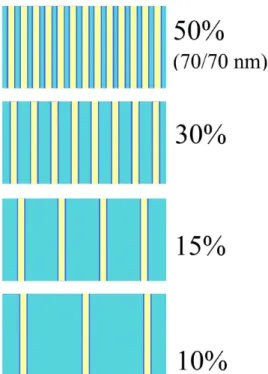
To investigate the area where process-induced damage was detected in the Cu/low-k structures, structural samples with different widths of the low-k spaces (S) and the height of the Cu lines (T) were investigated. We formed samples with different widths for the low-k spaces and Cu lines (L). Figure 3-3 shows the top view of the schematic Cu/low-k line and space structure with different space widths. The Cu line widths were 70 nm. In this study, line occupancy is defined as the ratio of the occupied area of a Cu line to the total area of Cu
- 41 -
lines and low-k spaces. The line occupancies were 10%, 15%, 30%, and 50%. In a different case, L and S were fixed at 70 nm, and T was varied to three different lengths: standard (100 nm), tall (125 nm), and short (75 nm).
- 42 -
RESULTS AND DISCUSSION
Figure 3-4 shows the IR transmittance to a Si substrate for L/S = 70/70 nm measured using different polarized IR light whose electric field component is (a) parallel and (b) perpendicular to the Cu lines. When the electric field component of the IR light was parallel to the Cu lines, the transmittance of IR light was less than 10%. In contrast, when the electric field component of the IR light was perpendicular to the Cu lines, the transmittance was almost 100%. This indicates that the Cu narrow lines work as an IR polarizer and only the electric field component of the IR light perpendicular to the Cu lines can pass through the Cu/low-k interconnect structure. The transmittance is observed to slightly exceed 100%. This phenomenon is considered to be caused by the refractive effect of IR through a silicon wafer with/without deposited films. Therefore, we determined a suitable measuring method that uses IR light whose electric field component is perpendicular to the Cu lines.
Figure 3-5 shows the IR spectra of a blanket film (non-patterning) and patterning samples (L/S = 70: 70 nm). The IR measurements were carried out using polarized IR light. The spectral shapes are similar to each other. It is very likely that the effect of Cu lines is non-existent, and thus, we can measure the Cu/low-k interconnect structure. The assignments of the main peaks of the low-k film are summarized in Table 3-I5, 8-11.
Figures 3-6(i) and (ii) display microscopic FT-IR spectra in the (i) 4000–700 cm-1 and (ii) 3800–2600 cm-1 regions for Cu/low-k samples with different spaces and line widths, respectively (Fig. 3-3). Each obtained spectrum reflects a different volume of low-k film components. Thus, we use the relative intensity of a band to the intensity of a band at 1050 cm-1 owing to the Si-O stretching mode, which is the main framework in the low-k film. The relative intensities of the bands due to the Si-CH3, Si-H, and OH stretching modes (Si-CH3:
- 43 -
shown in Fig. 3-7(i), (ii). The Si-OH peaks also appeared at approximately 900 cm-1 9-12 and are easily distinguishable from those owing to the OH groups derived from water. However, in the case of the low-k film, the peak of the Si-H bands is located around the same wavenumber as shown in Table 3-I. Thus, the peak intensity of the OH groups was estimated as the sum of the OH and the Si-OH peak area. The Si-H/Si-O intensity ratio is almost the same for all samples; however, the Si-CH3/Si-O intensity ratio decreases gradually as the
space width decreases. In addition, the OH/Si-O ratio significantly increases as the space width decreases. According to our previous report, the amount of Si-CH3 groups decreased
and its structure changed to a SiO2 network structure owing to the plasma processes23. It
appears that the generation of OH groups is related to process-induced damage; the volume fraction of the sidewall in the low-k film increases for narrower low-k space width.
Figure 3-8 shows the Si-O peak intensity obtained from Fig. 3-6. The absorption intensity of Si-O increases as the width of the low-k space reduces. This phenomenon appears to be due to an increase in the Si-O cross-linkage, as a result of process-induced damage. However, it is also likely that a localized electric field is generated between the Cu lines by the IR light. It may be caused by the surface-enhanced infrared absorption (SEIRA) phenomenon that has been reported so far13-16. The IR absorption of adsorbed species on gold, silver, and copper island films is enhanced; the degree of enhancement depends on the size of the islands and the gaps between islands. Thus, the Si-O peak intensity might be enhanced by SEIRA, and it might enable the sensitive detection of process-induced damage.
Figures 3-9(i) and (ii) depict microscopic FT-IR spectra in the (i) 1400–700 cm-1 and (ii) 3900–2600 cm-1 regions of the samples with different T (line and space widths of 70 nm) values. The T value is changed to three different heights—standard (100 nm), tall (125 nm), and short (75 nm)—to confirm the location of the damage in the low-k film. The relative peak intensities of Si-CH3, Si-H, and OH bands to that of the Si-O band at 1050 cm-1 are
- 44 -
shown in Fig. 3-10(i) and (ii). As T increases, the relative peak intensity of the OH groups increases. The number of OH groups was shown to correlate with the length of the side walls. We concluded that FT-IR spectra reflect mainly the structural changes such as process-induced damage in the sidewall of a low-k film.
It is presumed that the OH groups are generated in the low-k film when Si-CH3 bonds
break during the fabrication processes, and they are derived from atmospheric moisture, as shown in Fig. 3-11. As mentioned previously, process-induced damage was occurred in the side wall of low-k films, and the amount of Si-CH3 groups decreased. However, the
difference in the amount of the total Si-CH3 groups before and after the damage is small
because there are many Si-CH3 groups in the low-k films. The Si-OH groups are negligible in
the initial low-k film. Si-OH groups that were generated by the process-induced damage also draw moisture. Therefore, the total amount of OH groups is apparently amplified by the adsorption of water.
We attempted to evaluate the amount of carbon by EELS equipped with a low-voltage TEM. The measurement method is shown in Ref. 8. The carbon concentration mapping using EELS at the C-K edges is shown in Figure 3-12. If the depletion of carbon occurred in the sidewall of the low-k film, the color of the area would be denser than the other areas of the low-k film. However, the depletion of carbon was not clearly observed. The carbon detection limit of the TEM-EELS is approximately 0.5%. The composition errors were estimated to be ±2% and the space resolution was approximately 1 nm for the TEM-EELS. However, we detected Si-OH peaks by the FT-IR measurement for the same sample. The FT-IR can measure several sidewalls of the low-k films simultaneously and the Si-OH peak intensity is apparently amplified by the adsorption of water; it enabled a highly sensitive measurement of the process-induced damage for the sidewall of the low-k film and contributed to the revelation that the number of OH groups is a more sensitive indicator for a low-k damage
- 45 -
- 46 -
CONCLUSION
In the present study, the microscopic FT-IR spectra were measured for a Cu/low-k interconnect structure that had different widths of low-k spaces (S), widths of Cu lines (L), and heights of Cu lines (T) on Si substrates with polarized infrared light.
Based on the IR results, the effect of the direction of the electric field under IR light on the direction of the Cu line was investigated. We developed a suitable damage measuring microscopic FT-IR method using IR light whose electric field component is perpendicular to the Cu lines.
The microscopic FT-IR spectra for Cu/low-k samples with different space and line widths and samples with different T (line and space widths of 70 nm) were investigated. The results show that the process-induced damage that was detected by the FT-IR method is mainly reflected in the structural changes in the sidewall of a low-k film and the number of OH groups correlated with the length of the side walls. It is concluded that FT-IR spectra mainly reflect the process-induced damage in the sidewall of a low-k film.
Based on the discussion about process-induced spectral changes of low-k films, it is considered that the mechanism of generating process-induced damage involves the generation of the OH groups in the low-k film when Si-CH3 bonds break during the fabrication
processes and are derived from atmospheric moisture.
There are many Si-CH3 groups in the low-k films. However, OH groups are not excited in
the low-k film without damage. It was revealed that the number of OH groups was a more sensitive indicator for the low-k damage evaluation of the microscopic FT-IR method. We achieved the characterization of the process-induced damage that was not detected by the TEM-EELS. This may influence the reliability of the Cu/low-k interconnects. The method is applicable to narrow interconnects, e.g., those with line and space widths of 70 nm/70 nm or
- 47 -
less for advanced semiconductor processes.
Thus, the FT-IR study has provided us with novel and unique information regarding process-induced damage in Cu/Low-k interconnect structures.
- 48 -
REFERENCES
1N. Posseme, T. Chevolleau, T. David, M. Darnon, O. Louveau, and O. Joubert, J. Vac. Sci.
Technol. B 25, 1928 (2007).
2X. Hua, M. Kuo, G.S. Oehrlein, P. Lazzeri, E. Iacob, M. Anderle, C.K. Inoki, T.S. Kuan, P.
Jiang, and W. Wu, J. Vac. Sci. Technol. B 24, 1238 (2006).
3K. Yonekura, K. Yonekura, K. Goto, M. Matsuura, N. Fujiwara and K. Tsujimoto, Jpn. J.
Appl. Phys. 44, 2976 (2005).
4Y. Otsuka, Y. Shimizu, N. Kawasaki, S. Ogawa, and I. Tanaka, Jpn. J. Appl. Phys. 49,
111501 (2010).
5H. Seki, K. Inoue, N. Nagai, M. Shimada, K. Inukai, H. Hashimoto, and S. Ogawa, Proc.
AMC. 2004, pp. 375-380.
6S. Ogawa, H. Seki, Y. Otsuka, S. Nakao, Y. Takigawa, and H. Hashimoto, Proc. IITC, 2008,
pp. 76-78.
7H. Seki, N. Tarumi, Y. Shimizu, Y. Otsuka, H. Hashimoto, and S. Ogawa, Proc. AMC, 2008,
pp. 647-650.
8A. Grill and D.A. Neumayer, J. Appl. Phys. 94, 6697 (2003).
9C.Y. Wang, J.Z. Zheng, Z.X. Shen, Y. Lin, and A.T.S. Wee, Thin Solid Films. 397, 90
(2001).
10W.A. Pliskin, J. Vac. Sci. Technol. 14, 1064 (1977).
11K. M. Davis, M. Tomozawa, J. Non-Cryst. Solids. 201, 177 (1996).
12S. Sugahara, T. Kadoya, K. Usami, T. Hattori, and M. Matsumura, J. Electrochem. Soc. 148,
F120 (2001).
13A. Hartstein, J.R. Kirtley, and J.C. Tsang, Phys. Rev. Lett. 45, 201 (1980). 14M. Osawa, Bull. Chem. Soc. Jpn. 70, 2861 (1997).
- 49 -
- 50 -
Table. 3-I. Peak assignments of an IR spectra of a porous SiOC film. Peak
position(cm-1) Assignments Comment
3650 ν Si-OH Due to damage
3300 ν OH adsorbed water 2970 ν C-CH3 Si-(CH3)x 2240 ν Si-H H-SiO3 2180 ν Si-H H-SiO2Si 1640 δ OH adsorbed water 1410 δs C-CH3 Si-(CH3)x 1360 δ C-CH2 Si-CH2-Si 1270 δa C-CH3 Si-(CH3)x 1140 νa Si-O-Si Cage 1050 νa Si-O-Si Network
950-900 δ Si-OH Due to damage
890 δ Si-H H-SiO3
840 ρa CH3 Si-(CH3)3
800 ρa CH3 Si-(CH3)2
780 ρa CH3 Si-(CH3)1
- 51 -
Fig. 3-1 Schematic view of the sample structure. Cu line width (L), low-k space width (S) were changed while keeping Cu line (T) constant, and the height of the Cu lines (T) was changed keeping Cu line width (L) and low-k space width (S) constant.
- 52 -
Fig. 3-2 Schematic view of the polarized IR absorption measurement. The electric field component of IR light is (a) parallel and (b) perpendicular to the Cu lines.
- 53 -
Fig. 3-3 Schematic view of the sample structure with different line occupancies (top view). Line width was fixed at 70 nm and line occupancies were varied: 10%, 15%, 30%, and 50%.
- 54 -
4000
3500
3000
2500
2000
1500
1000
0
20
40
60
80
100
120
140
T
ra
n
sm
it
ta
nc
e(
%
)
Wavenumber(cm
-1)
Fig. 3-4 IR transmittance to the Si substrate for L/S = 70/70 nm using different polarized IR light whose electric field component is (a) parallel and (b) perpendicular to the Cu lines.
(b) E
⊥
(a) E
- 55 -
4000 3500 3000 2500 2000 1500 1000 -0.15 -0.10 -0.05 0.00 0.05 0.10 0.15 0.20 0.25 (b) Cu /Low-k structure (a) blanket filmA
b
so
rb
an
c
e
Wavenumber (cm
-1)
Fig. 3-5 IR spectra of (a) a blanket film and (b) Cu/low-k structure (L/S = 70 nm:70 nm). IR measurements were carried out using polarized IR light.
- 56 -
Fig. 3-6 FTIR spectra of Cu/low-k samples with different line widths and space structures: (i) FTIR spectra in the region of 4000–700 cm-1. (ii) FT-IR spectra in the 3800–2600 cm-1 region.
- 57 -
Fig. 3-7 Ratio of FT-IR peaks intensities: (i) Si-CH3 and Si-H, (ii) OH.
(i)
- 58 -
- 59 -
Fig. 3-9 FT-IR spectra for Cu/Low-k samples with different Cu line heights: (a) standard (b) short (c) long (L/S = 70 nm/70 nm). (i) in the 1400–700 cm-1 region and (ii) in the 3900–2600 cm-1 region.
- 60 -
Fig. 3-10 Ratio of FT-IR peak intensities: (i) Si-CH3 and Si-H, and (ii) OH.
(i)
- 61 -
- 62 -
- 63 -
Chapter 3
Characterization of Inhomogeneity in SiO2 Films on 4H-SiC Epitaxial Substrate by a
- 64 -
ABSTRACT
We measured the Fourier transform infrared (FT-IR) and cathodoluminescence (CL) spectra of SiO2 films grown on 4H-SiC substrates and confirmed that the phonon observed at
around 1150–1250 cm-1 originates from the upper branch of the surface phonon polaritons (SPPs) in the SiO2 films and that its frequency is sensitive to the oxide thickness. The relative
intensity of the upper branch of SPPs normalized by that of the transverse optical phonon (TO) tended to increase with decreasing channel mobility (CM). A comparison between the FT-IR and CL measurements shows that the relative intensity is correlated with an inhomogeneity in the SiO2/SiC interface, and the CM of SiC devices. A combination of
FT-IR and CL spectroscopy provides us with a large amount of data on the inhomogeneity, defect, and oxide thickness of SiO2 films on 4H-SiC substrates.
- 65 -
INTRODUCTION
Silicon carbide (SiC) is a well-known wide-bandgap semiconductor for high-power, high-frequency metal–oxide–semiconductor (MOS) device applications. The high interface trap densities (Dit) at the SiO2/SiC interface and the high effective fixed charge densities
(Qeff), which are one to two orders of magnitude higher than those typically found at the
SiO2/Si interface (of the order of 1011 cm-2),1 degrade the channel mobility (CM).2–5 The
presence of interface traps in SiC MOS field-effect transistors (FETs) is attributed to (i) excess carbon,4,6 (ii) interface defects due to the presence of threefold coordinated O and C interstitial atoms,4,6 and (iii) point defects such as Si and O vacancies that extend into the SiC layer underneath the SiO2/SiC interface.7,8 H2,2 NO,9,10 or N2O3,11–13 post-oxidation annealing
(POA) effectively increases.
Fourier transform infrared (FT-IR) spectroscopy is an effective tool for investigating chemical bonding structures in thin oxide films. However, we cannot measure the transparent FT-IR spectra of SiO2 films prepared on commercially available 4H-SiC substrates because
of the strong absorptions due to the free carriers in the substrates. As a result, the attenuated total reflection (ATR) configuration is used as a highly sensitive method for investigating the SiO2 films.14 Transverse optical (TO) and longitudinal optical (LO) phonons in thermally
grown SiO2 films on a Si wafer have been observed at around 1072 and 1257 cm-1,
respectively.8 These phonons are associated with the asymmetrical stretching of O in the intertetrahedral Si-O-Si bridge.9 Although many studies have reported FT-IR spectroscopy of thermally grown SiO2 films on Si wafers, none have focused on the microstructures in the
interface between SiO2 films and SiC wafers.10,11
Figure 4-1 shows the normal and grazing incidence and ATR spectra of a thick (100 nm) SiO2 film on a bulk epitaxial 4H–SiC substrate15. We reported abnormal behavior of LO