Japan Advanced Institute of Science and Technology
JAIST Repository
https://dspace.jaist.ac.jp/
Title
Hole-injection barrier in pentacene field-effect
transistor with Au electrodes modified by
C_16H_33SH
Author(s)
Kawasaki, Naoko; Ohta, Yohei; Kubozono,
Yoshihiro; Fujiwara, Akihiko
Citation
Applied Physics Letters, 91(12):
123518-1-123518-3
Issue Date
2007-09
Type
Journal Article
Text version
publisher
URL
http://hdl.handle.net/10119/3993
Rights
Copyright 2007 American Institute of Physics.
This article may be downloaded for personal use
only. Any other use requires prior permission of
the author and the American Institute of Physics.
The following article appeared in N. Kawasaki,
Y. Ohta, Y. Kubozono, and A. Fujiwara, Applied
Physics Letters 91(12), 123518 (2007) and may be
found at http://link.aip.org/link/?apl/91/123518.
Hole-injection barrier in pentacene field-effect transistor with Au electrodes
modified by C
16H
33SH
Naoko Kawasaki, Yohei Ohta, and Yoshihiro Kubozonoa兲
Research Laboratory for Surface Science, Okayama University, Okayama 700-8530, Japan
Akihiko Fujiwara
Japan Advanced Institute of Science and Technology, Ishikawa 923-1292, Japan
共Received 21 July 2007; accepted 4 September 2007; published online 21 September 2007兲 Field-effect transistor with thin films of pentacene has been fabricated with Au electrodes modified by 1-hexadecanethiol 共C16H33SH兲, and the hole-injection barriers have been determined from the temperature dependence of output properties on the basis of the thermionic emission model for double Schottky barriers. The large tunneling barriers are formed by the insulating C16H33SH at the interfaces between the Au electrodes and pentacene thin films. © 2007 American Institute of Physics. 关DOI:10.1063/1.2789699兴
Interface control is a very important technique for the realization of high-performance field-effect transistor共FET兲 devices. Recently, the Fermi level matching of the source/ drain electrodes to the conduction/valence band of organic active layers produced n-, p-, and ambipolar FET properties.1–3These results opened the possibility of the FET devices with organic molecules. We also observed high value of 0.5 cm2V−1s−1 in the C60 FET with the Eu
elec-trodes which possess low work functionof 2.5 eV.4This contact material has produced the Ohmic contact or effective carrier injection between the electrodes and C60thin films.
In order to clarify the mechanism of carrier injection from electrodes to active layers, we analyzed the transport properties of the C60FET devices with Au electrodes
modi-fied by 1-alkanethiols共CnH2n+1SH兲 on the basis of the
ther-mionic emission model for double Schottky barriers.5,6 The effective Schottky barrier heightB
eff
and tunneling efficiency of electron for alkyl chains were determined and the elec-tronic structures at the interface between the electrodes and C60thin films were fully investigated. TheBeffcontains
con-tributions from both Schottky barrier of pure Au– C60
junc-tion and addijunc-tional tunneling barrier formed by CnH2n+1SH.
However, the Schottky barrier and the tunneling of the hole through alkyl chains at the interface of the p-channel organic FET devices have not been investigated so far.
In this study, we have investigated hole injection from the Au electrodes to pentacene thin films within the frame-work of thermionic emission model for double Schottky barriers.5,6The pentacene thin-film FET device with Au elec-trodes modified by 1-hexadecanethiol 共C16H33SH兲,
pentacene/C16H33SH FET, showed large effective hole-injection barrierbheffand it allowed us to provide useful in-formation on Au-pentacene junctions in the FET device.
The device structure is shown in Fig.1共a兲; the details of the dimensions are shown in the caption of Fig. 1共a兲. The processes for a cleaning of the surface of Si共100兲/SiO2
wa-fers and for the formation of Au electrodes are described elsewhere.5,6The surface of Au electrodes was modified with C16H33SH by immersing the Si/ SiO2/ Cr/ Au substrates into the ethanol共EtOH兲 solution of C16H33SH 共10−1mol l−1兲 for
47 h. The molecular structure of C16H33SH is shown in Fig.
1共b兲. The substrates were washed with EtOH and ultrapure H2O. The expected structure of C16H33SH on the Au
surface7,8 is shown in Fig. 1共c兲. The thin films 共50 nm兲 of pentacene were formed on the substrate maintained at room temperature T by a thermal deposition under vacuum of 10−8Torr. The transport characteristics of the FET devices
were measured under vacuum of 10−6Torr without
anneal-ing of the devices.
a兲Electronic mail: [email protected]
FIG. 1.共Color online兲 共a兲 Device structure of pentacene thin-film FET. The thicknesses of Cr, Au, and pentacene are 5, 50, and 50 nm, respectively. The channel width W and length L are 4000 and 30m, respectively. The thick-ness and capacitance C0of SiO2are 400 nm and 8.63⫻10−9F cm−2,
respec-tively.共b兲 Molecular structures of C16H33SH.共c兲 Schematic representation
of the surface of Au electrodes modified by C16H33SH. APPLIED PHYSICS LETTERS 91, 123518共2007兲
0003-6951/2007/91共12兲/123518/3/$23.00 91, 123518-1 © 2007 American Institute of Physics
The absolute drain current 兩ID兩 versus absolute
source-drain voltage 兩VDS兩 plots of the pentacene/C16H33SH FET
device show p-channel normally off FET properties 关Fig. 2共a兲兴. The 兩ID兩-兩VDS兩 plots also show clear concave-up
non-linear behaviors in the low VDSregion, which shows that the
hole transport is strongly suppressed by the large effective hole-injection barrierbheff. The 兩ID兩 increases linearly in the intermediate region for the pentacene/C16H33SH FET 关Fig.
2共a兲兴 and saturates in the high VDSregion.
The values ofand VTwere determined from the drain
current 兩IDsat兩 in the saturation region 共VDS= 100 V兲, i.e., 兩IDsat兩1/2versus absolute gate voltage 兩VG兩 plot 关Fig. 2共b兲兴, to
be 6.8⫻10−4cm2V−1s−1 and 35 V at 300 K, respectively.
The value is lower by one order of magnitude than the value, 5.9⫻10−3 cm2V−1s−1, of C
60/ C16H33SH FET.
5 The absolute drain current density兩JD兩 vs 兩VDS兩 plot in the low
VDS region 共0–20 V兲 at VG= 100 V for the pentacene/
C16H33SH FET device共T=300 K兲 is shown in Fig.2共c兲 to-gether with the calculated共fitting兲 line. The fitting line was drawn according to Eq.共1兲based on the thermionic emission model expanded to double Schottky barriers because this de-vice possesses two Au-pentacene junctions modified by C16H33SH 共source Au electrode-pentacene and pentacene–
drain Au electrode兲,5 JD= A*T2 ⫻exp共−bh eff /kBT兲sinh关eVDS/共2kBT兲兴/cosh共eVDS/2nkBT兲, 共1兲 where A*, e, and kB are the effective Richardson constant,
electron charge, and Boltzmann constant, respectively. The A* and
bh
effare given by Eqs.共2兲and共3兲, respectively,
A*= 4emp * kB 2 /h3 共2兲 and bheff=bh+ kBThl. 共3兲 Here mp *
, h, bh, h, and l are the effective mass of hole,
Planck’s constant, hole-injection barrier height of pure Au-pentacene junction, tunneling efficiency of hole, and length of tunneling barrier, respectively. In the analyses, the mp*was fixed to be 1.55m0based on the value reported previously;9
m0 is the electron rest mass. The term kBT hl in Eq. 共3兲
refers to the additional tunneling barrier produced by inser-tion of C16H33SH.
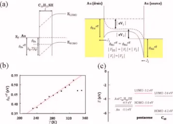
The energy band diagram for the Au-pentacene junction modified by C16H33SH and the simplified energy diagram for
two junctions under the application of VDS is shown in Fig.
3共a兲. In this model, most of VDSis assumed to be applied to
the interfaces of the two junctions because the channel resis-tance is small at VG= 100 V 共⬎VT of 35 V兲 in comparison
with the contact resistance. In the estimation of JD, the
thick-ness of channels is assumed to be 1 nm based on Ref.10. The bheff value at 300 K was determined to be 0.467± 0.003 eV by least-squares fitting to the JD-VDS plot
共0–20 V兲 with Eq. 共1兲. The n value at 300 K was 1.0043± 0.0002. This value is close to the ideal value of unity, suggesting that two junctions of this device are almost ideal Schottky diodes. Thebheffvalue is smaller than theB
eff
共=0.51±0.02 eV兲 determined for the C60/ C16H33SH FET.5,6
In the 兩ID兩-兩VDS兩 plots 共VG= 100 V兲 at 230–350 K for
pentacene/C16H33SH FET, the large concave-up nonlinearity
in the low VDSregion is observed in the plots at low T region
共not shown兲. Thebh eff
value was determined from the JD-VDS
plot of VDS= 0 – 20 V at VGof 100 V at each T with Eq.共1兲.
FIG. 2.共Color online兲 共a兲 兩ID兩-兩VDS兩, 共b兲 兩ID sat兩1/2-兩V
G兩, and 共c兲 兩JD兩-兩VDS兩 plots
of pentacene/C16H33SH FET at 300 K. The fitted lines are drawn for 共b兲
with共兩IDsat兩兲1/2=共WC
0/ 2L兲1/2共兩VG兩−兩VT兩兲 and for 共c兲 with Eq.共3兲.
FIG. 3.共Color online兲 共a兲 共Left兲 Schematic representation of band bending for pentacene-Au junction modified by C16H33SH and共right兲 that of band
bending共solid line兲 for double Schottky barriers in pentacene/C16H33SH
FET. In the right figure, the additional tunneling barriers due to C16H33SH are not drawn.共b兲bheff− T plot for pentacene C16H33SH/FET.共c兲 Band
dia-gram of EFof Au, EHOMO, and ELUMOof pentacene and C60.
123518-2 Kawasaki et al. Appl. Phys. Lett. 91, 123518共2007兲
Thebheff-T plot is shown in Fig.3共b兲. As expected from Eq. 共3兲, the linear relationship was observed in the bheff-T plot below 340 K. The values at 340 and 350 K deviate from the line. This corresponds to the variation from concave-up non-linear ID-VDS curve to linear line above 330 K, which
sug-gests that the hole-injection barrier is gradually destroyed because of the thermal fluctuation of C16H33SH on Au electrodes.
The bh and h values for pentacene/C16H33SH FET
have been determined by least-squares fit tobheff-T plot关Fig. 3共b兲兴 with Eq. 共3兲. When the l, 18.6 Å, of C16H33S – Au is
used as the length to the tunneling barrier in this analysis 关Figs.1共c兲and3共a兲兴,8the h value can be determined to be
0.91± 0.03 Å−1, whose value is almost the same as the 
value, 1.12± 0.06 Å−1, for electron in C60/ C16H33SH FET.5,6
This implies that the efficiency of the carrier tunneling across the CH2chain is not much different for electrons and holes.
If a vacuum barrier was assumed between Au and pentacene, theh would be estimated to be 2.28 Å−1 since the highest
occupied molecular orbital共HOMO兲 level, EHOMO, of
penta-cene and the EF of Au modified by C16H33SH is −5.0 and
−4.9 eV, respectively, as seen from Fig.3共c兲1,5Thishvalue
of 2.28 Å−1 is more than two times larger than the
experi-mental value 共0.91±0.03 Å−1兲. This result implies that the holes can pass through the C16H33S – Au more easily than
through the vacuum barrier.
The bh value can be determined from the bh eff
-T plot 关Fig.3共b兲兴 to be 0.03±0.01 eV. This value is smaller than that, 0.09± 0.03 eV, determined from thebeff-T plot for the
C60/ C16H33SH FET.5From the band diagram of Au and
pen-tacene, for holes, the Schottky barrier height between Au and pentacene can be expected to be 0.1 eV 关Fig. 3共c兲兴, whose value is slightly larger than the experimental bh value of
0.03± 0.01 eV determined in this study. The deviation of ex-perimentalbhfrom the value expected from the simple band
picture may be due to the lowering of actual Schottky barrier height produced by interface states, mirror charge effect, and electric double layer formed at the interface. However, this deviation is much smaller than the case of Au– C60junctions
共experimental B: 0.09 eV, the Schottky barrier height
ex-pected from simple band picture: 1.5 eV兲.5
In conclusion, the JD-VDS curves of the pentacene/ C16H33SH FET could be analyzed reasonably well within the
thermionic emission model for double Schottky barriers, and the reliable values ofbh andh have been determined for
the FET device. In the pentacene/C16H33SH FET device,
more than 90% in thebheffat 300 K is contributed from the additional tunneling barrier, which is associated with the tun-neling of hole through C16H33SH insulators inserted into the
Au-pentacene junctions. As the reliable parameters for the Schottky barrier heights in the p-channel pentacene FET de-vices are obtained by the application of thermionic emission model for double Schottky barriers to the JD-VDS curves in
the same manner as the case of n-channel C60 FET,5,6 this
analysis has been shown to be useful for the investigation of carrier injections in both n- and p-channel organic FET devices.
This study was partly supported by a Grant-in-Aid 共18340104兲 from MEXT, Japan.
1T. Yasuda, T. Goto, K. Fujita, and T. Tsutsui, Appl. Phys. Lett. 85, 2098
共2004兲.
2T. Nishikawa, S. Kobayashi, T. Nakanowatari, T. Mitani, T. Shimoda, Y.
Kubozono, G. Yamamoto, H. Ishii, M. Niwano, and Y. Iwasa, J. Appl. Phys. 97, 104509共2005兲.
3Y. Takahashi, T. Hasegawa, Y. Abe, Y. Tokura, and G. Saito, Appl. Phys.
Lett. 88, 073504共2006兲.
4K. Ochi, T. Nagano, T. Ohta, R. Nouchi, Y. Kubozono, Y. Matsuoka, E.
Shikoh, and A. Fujiwara, Appl. Phys. Lett. 89, 083511共2006兲.
5T. Nagano, M. Tsutsui, R. Nouchi, N. Kawasaki, Y. Ohta, Y. Kubozono,
and N. Takahashi, A. Fujiwara, J. Phys. Chem. C. 111, 7211共2007兲.
6Y. Ohta, N. Kawasaki, T. Nagano, R. Nouchi, Y. Kubozono, and A.
Fujiwara共unpublished兲.
7C. Schönenberger, J. Jorritsma, J. A. M. Sondag-Huethorst, and L. G. J.
Fokkink, J. Phys. Chem. 99, 3259共1995兲.
8D. M. Alloway, M. Hofmann, D. L. Smith, N. E. Gruhn, A. L. Graham, R.
Colorado Jr., V. H. Wysocki, T. R. Lee, P. A. Lee, and N. R. Armstrong, J. Phys. Chem. B 107, 11690共2003兲.
9M. Nakamura, Abstract of IMR Symposium of Tohoku University, 2007
共unpublished兲, p. 10.
10T. Miyadera, M. Nakayama, and K. Saiki, Appl. Phys. Lett. 89, 172117
共2006兲.
123518-3 Kawasaki et al. Appl. Phys. Lett. 91, 123518共2007兲