日本熱電学会誌 第 16 巻第 3 号(2020)144-149
自己組織的に転位を導入した CrSi
2
/Si コンポジットの熱
電特性
大石 佑治
1*,江畑 大輝
1,牟田 浩明
1,黒崎 健
2 1 大阪大学 大学院工学研究科,〒 565-0871 大阪府吹田市山田丘 2-1 2 京都大学 複合原子力科学研究所,〒 590-0494 大阪府泉南郡熊取町朝代西 2-1010The Journal of the Thermoelectrics Society of Japan Vol. 16, No. 3 (2020), pp. 144-149 Ⓒ 2020 The Thermoelectrics Society of Japan
Thermoelectric properties CrSi
2/Si composite with naturally decorated dislocations
Yuji Ohishi
1*, Daiki Ebata
1, Hiroaki Muta
1, Ken Kurosaki
21 2-1 Yamadaoka, Suita, Osaka 565-0871, Japan, Graduate School of Engineering, Osaka University
2 2-1010 Asashiro-nishi, Kumatori-cho, Sennan-gun, Osaka, 590-0494, Japan, Institute for Integrated Radiation and Nuclear Science, Kyoto University
Si is a promising candidate for environmentally friendly thermoelectric (TE) material because of its non-toxicity and abundance. However, the lattice thermal conductivity of Si is extremely high, leading to low dimensionless figure of merit ZT. In a previous study, Xie et al. succeeded in reducing lattice thermal conductivity and improving
ZT (0.39 at 1073 K) by forming dense dislocations in CoSi2/Si composite. These dislocations were automatically
introduced into Si matrix by sintering melt-spun powders. The formation mechanism of the dislocations is considered to be related to the eutectic reaction between CoSi2 and Si. In this study, we applied the same process to Cr-Si system, which has similar eutectic temperature and eutectic composition to Co-Si system, intending to get insight into the formation mechanism of the dislocations. P-doped n-type Si and CrSi2 nanocomposites were synthesized by melt spinning followed by spark plasma sintering. Transmission electron microscope observation showed that there were dislocations in Si matrix that seems to be formed by the same mechanism with CoSi2/Si. Owing to the reduced lattice thermal conductivity, the maximum ZT reached 0.37 at 1073 K. This result indicates that a eutectic reaction plays an important role in the formation of the dislocations.
(Received: October 24, 2019; Accepted: January 17, 2019; Published online: January 22, 2019)
Keywords: self-assembled nanostructure; lattice thermal conductivity; Si-based thermoelectric material; melt-spinning; spark plasma
sintering
1.は じ
め
に
Si は代表的な環境調和型熱電材料であり,構成元素の希 少性や毒性といった面では一般的な高性能熱電材料に対して 大きな利点を有している.単結晶 Si(n 型:6.8×1019 cm−3, p 型:1.1×1020 cm−3)の熱電性能は既に報告されており1), 出力因子は 600-900 K においてそれぞれ 4.4 mWm−1K−2と 2.6 mWm−1K−2と比較的高い値を有している.しかしながら, 熱伝導率は n 型,p 型ともに室温において 80 Wm−1K−1程度 と熱電材料としては極めて高い値となっており,これが原因 で性能指数 ZT の最大値は n 型では 0.17,p 型では 0.10 程度 となっている. 熱伝導率は,ナノ構造化によってフォノンを散乱させるこ とで低減できることが知られている.そのため,Si でも多 くのナノ構造化の試みがなされてきた.これまでに,ナノ結 晶2-4)やナノワイヤー5, 6),ナノメッシュ7, 8)構造の Si において 大幅な熱伝導率の低減と ZT の向上が達成されている.特に リソグラフィー技術を用いて作製されたナノワイヤー Si に おいては,ZT は 200 K において 1 に達している5). このように Si はナノ構造化によって大幅な熱電性能の向 上が可能であることは既に実験的に示されているが,熱電材 料を実用化するためには一般的にバルクサイズの材料が必要 であり,リソグラフィーのような技術はバルク材料の作製に は不向きである.すなわち,Si を熱電材料として広く用い るためには,ナノ構造をバルク材料中に導入する技術の開発 が課題となっている. ナノ構造を自己組織的に構築することができれば,ナノ構 造を有するバルク材料の実現が可能である.我々のグループ では自己組織的なナノ構造の構築を目指し,共晶組成の合金 の液体急冷法による急冷9, 10)やアモルファスからの結晶相の 生成11–13)等を試みてきた.近年,Si に固溶度以上 P を加えて アーク溶解し,放電プラズマ焼結法 (SPS)によって焼結す ることでナノサイズの析出物が形成されること,及び熱電性第 3 号 自己組織的に転位を導入した CrSi2/Si コンポジットの熱電特性 145 能が向上することを見出した14).さらに Co を加えて(Si-P-Co)焼結することで,析出物に加えて転位を導入することが でき,熱電性能をさらに向上させることができることを示し た(1045 K において ZT=0.39)15).ナノ析出物を形成させて 熱電性能を向上させるという試みは多くみられるが,転位の 導入により熱電特性の向上を試みたというのは筆者の知る限 り他に例はない.転位は元素置換やナノ析出物と組み合わせ ることが可能であるため,Biswas らによって提唱された all-scale hierarchical architectures16)を実現できる可能性がある と考えられる. 転位の生成メカニズムはまだ明らかになっていないが, Si-P-Co の先行研究では SPS による焼結温度が低くても高く ても転位は発生せず,最適な焼結温度の時にのみ転位が生じ て熱電性能が向上した.その最適な焼結温度は Si-CoSi2の 共晶温度と近い温度である.すなわち,焼結中に試料の一部 が共晶反応によって溶融することが転位生成の原因である可 能性がある.そこで共晶反応が転位の生成に重要な役割を 担っているという考えを検証するため,Si-CoSi2(共晶温度: 1533 K17))と共晶温度が近い Si-CrSi2(共晶温度:1578 K18)) に着目し,Co の代わりに Cr を用いた場合にも転位の形成 と熱電特性の向上が可能であるかを確かめることを本研究の 目的とした.
2. 実 験 方 法
Si-P-Co の先行研究では,P は Si に対して 3% 加え,Co を Si と P に 対 し て 5% 加 え た (Si0.97P0.03)0.95Co0.05の 組 成 で試験を行った15).そこで,本研究における試料組成は (Si0.97P0.03)0.95Cr0.05とした.Si-Cr 状態図によると Si へ Cr はほ ぼ固溶しないので,この組成では Si と CrSi2のコンポジット となると考えられる.Si-P-Co の先行研究と同様にアーク溶 解によってインゴットを作製し,得られたインゴットを液体 急冷法によって急冷した後に SPS で焼結して試料を作製し た.最適な焼結温度を見出すために,焼結温度をパラメータ として変化させた.その後,相状態評価,微細組織観察,及 び物性評価を行った. Si (半導体グレード,大阪チタニウム),Cr(3N,高純度 化学研究所),P(6N,フルウチ化学)を (Si0.97P0.03)0.95Cr0.05 の組成比となるよう秤量し,Ar 雰囲気下でアーク溶解を行っ た.得られたインゴットを銅ロール液体急冷法によって液体 急冷(Ar 雰囲気,ノズル径 f0.60 mm,ロール回転速度,銅 ロール / ノズル間ギャップ 0.20 mm,噴射圧 0.02 MPa)し, 続いて SPS により Ar フロー雰囲気下,圧力 100 MPa で焼 結した.焼結温度を 1273 から 1473 K まで変化させることで, #1-6 の 6 種類のバルク試料を作製した.試料番号と焼結温 度の関係は Table 1 に示してある.なお,試料 #6 を焼結す る際,試料の一部が溶融し試料外部に押し出される様子が観 察された(Fig. 1)ことから,1473 K 以上の温度での焼結は 行わなかった. 作製した試料について,粉末 X 線回折(XRD)測定によ り結晶相の同定を行った(Ultima-IV,Rigaku).格子定数は, 測定した XRD パターンのピーク位置から Whole PowderPattern Fitting Method を用いて計算した.ピーク位置は NIST Si を用いて校正した.格子定数から計算した理論密度 と実測密度から,相対密度を算出した.また試料表面の微細 構造観察及び元素分析を,走査型電子顕微鏡(SEM)(JSM-6500F, JEOL)とエネルギー分散型 X 線分析(EDS)装置 (EX-64175JMU, JEOL)を用いて行った.また,透過型電子 顕微鏡(TEM)(H-9500,日立ハイテクノロジーズ)を用い て転位の観察を行った. 各 試 料 の キ ャ リ ア 濃 度 は, ホ ー ル 効 果 測 定 シ ス テ ム (Resitest-8340,東陽テクニカ)を用いて測定した.電気抵 抗率 ρ は 4 端子法により,ゼーベック係数 S は定常直流法 により測定した(ZEM-3,アドバンス理工).事前に同装置 で標準試料 (コンスタンタン)の測定を行い,文献値に対し て電気抵抗率の測定値は±4%,ゼーベック係数の測定値は ±5% の範囲内であることを確認した.測定は各温度で 3 回 以上行い,標準誤差を図中にエラーバーで示した.また熱 拡散率 α をライトフラッシュ法を用いて測定した (LFA467, NETZSCH).これも事前に同装置を用いて標準試料 (等方 性黒鉛標準試料)の測定を行い,文献値に対する測定値は± 5% の範囲内であることを確認した.α の測定値を用い,熱 伝導率 κ を κ=α・Cp・d により導出した.ここで d は密度, Cpは比熱容量である.比熱容量は Si と CrSi2の文献値を元
に,Si と CrSi2のモル分率から計算した.格子熱伝導率 klatは, ウィーデマン・フランツの法則に基づき κ=κlat+κele,κele=L・
T/ρ(L=2.44×10−8 WΩK−2)によって計算した.ここで σ は電気伝導率,T は絶対温度である.
3.結果と考察
Figure 2 (a)に,作製試料の粉末 X 線回折パターンを示す. 本研究で作製した全ての試料で,Si19)及び CrSi220)の文献値と 一致するピークが確認された.その他の不純物は確認されな かった.Figure 2 (b)に CrSi2のメインピーク(43°)付近を拡大した図を示す.試料 #6(焼結温度:1473 K)は CrSi2 相に起因するピークの強度が他の試料(焼結温度:1273-1443 K)と比較して著しく低下していることが分かる.これ は,焼結中に CrSi2が Si と共晶反応を起こして溶融し,試料 外部に押し出されてしまった(Fig. 1)ことによるものと考 えられる. Table 1 には,各試料の焼結温度と相対密度,及びキャリ ア密度の値を示してある.なお試料 #6 については,CrSi2相 が全て試料外部に押し出されたと仮定し,相対密度を算出し た.焼結温度が最も低い #1 の試料の相対密度が最も低かっ たが,いずれの試料についても相対密度が 90% を超える緻 密な試料が得られた.また,キャリア密度は 3–5×1020cm−3 程度であった.
続いて,Fig. 3 には液体急冷後の試料表面の,Fig. 4(a)- (f)には SPS 後の試料 #1-#6 の試料表面の SEM 画像をそれ ぞれ示す.これらの画像において,暗い領域は Si 母相,明 るい領域は CrSi2析出相である.液体急冷後の試料表面の SEM 画像からは,Si 母相中におよそ 10 nm 程度の大きさの CrSi2析出相が分散している様子が見て取れる.一方で SPS 後の試料については,いずれの温度で焼結した試料もおよ Table 1. Sintering temperatures and relative densities of
(Si0.97P0.03)95Cr5 samples.
No. Sint. temp. (K) Relative density(% T.D.) Carrier density(cm−3)
#1 1273 91 2.7 × 10²⁰ #2 1323 98 2.6 × 10²⁰ #3 1373 95 2.9 × 10²⁰ #4 1423 96 4.9 × 10²⁰ #5 1443 95 3.9 × 10²⁰ #6 1473 99 −
Fig. 2. (a) Powder XRD patterns of (Si0.97P0.03)95Cr5 samples, and (b)
enlarged patterns at 2θ=42-44 .
Fig. 3. SEM image of the sample after melt-spinning.
Fig. 4. SEM images of the bulk samples sintered at (a) 1273 K to (f) 1473 K.
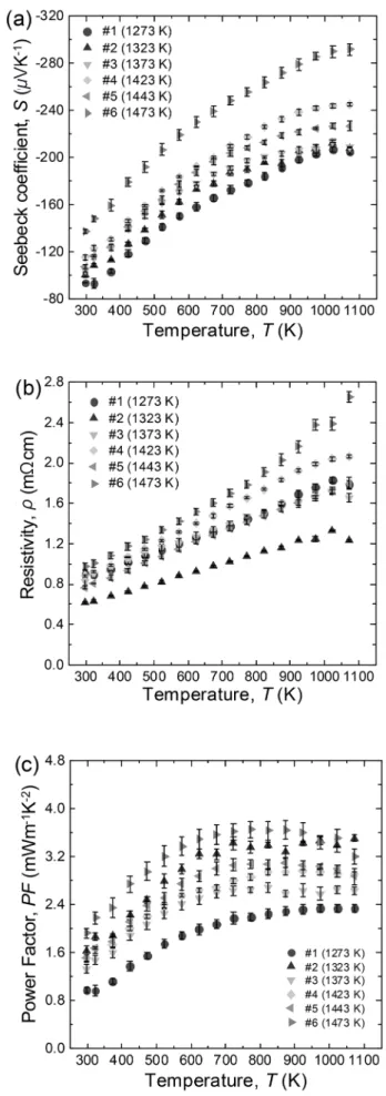
第 3 号 自己組織的に転位を導入した CrSi2/Si コンポジットの熱電特性 147 そ 5-10 mm 程度の CrSi2相が母相中に均一に分散しており, SPS により CrSi2相がおよそ 103倍のサイズまで粒成長して いることが分かる. 焼結温度による CrSi2相のサイズへの顕著な影響は見られ なかった.なお,#6 の試料には CrSi2析出物は見られなかっ た.これは先に示した XRD の結果と整合しており,焼結温 度が高いために CrSi2が Si と共に溶融して試料外に押し出さ れたためであると考えられる. Figure 5 にそれぞれの試料の(a)ゼーベック係数 S,(b) 電気抵抗率 ρ,及び(c)パワーファクター PF=S2⁄ ρ の温度 依存性を示す.Si は全ての試料は負のゼーベック係数を示 しており,添加した P は Si において n 型のドーパントであ るために妥当な結果である.焼結温度が最も高い #6 の試料 が最も高いゼーベック係数の値を示した.母相である Si は n 型であるが CrSi2は p 型の半導体であるため,CrSi2の存 在はゼーベック係数を低下させると思われる.#6 の試料は CrSi2相がほとんど含まれていないので,最も高いゼーベッ ク係数を示したものと思われる. 電気抵抗率は多少のばらつきはあるものの #6 と #2 以外は 概ね同程度の値となった.Table 1 に示す通り #2 の試料は #6 を除くと最も相対密度が高く,これが低い電気抵抗率を示す 原因であると考えられる.この低い電気抵抗率が大きく寄与 し,パワーファークターは #6 を除くと #2 が最も高くなった. Figure 6(a)に,熱伝導率の温度依存性を示す.全ての 試料は温度上昇とともに熱伝導率が低減するという半導体的 な挙動を示した.#6 の試料が最も高い熱伝導率を示したの は,焼結温度が最も高く CrSi2相がほとんど消失したためで あると思われる.一方,#6 以外の試料においても焼結温度 が低下するに従って熱伝導率が低下する傾向が見られた. 焼結温度の影響を評価するために,室温における格子熱伝 導率を焼結温度に対してプロットした図を Fig. 6(b)に示す. 焼結温度の低下とともに格子熱伝導率は低減し,焼結温度が 1273-1373 K のときに格子熱伝導率は 15-20 Wm−1K−1程度 となっていることが分かる.この値は Si-P-Co における格子 熱伝導率(13.5 W/mK15))と近い値であり,Si-P-Cr 系にお いても Si-P-Co と同程度まで格子熱伝導率を低減させること ができた. 格子熱伝導率の低減が転位によるものであるとすると, Si-P-Cr においては 1273-1373 K が転位の生成に適した焼結 温度であると言える.転位の有無を確かめるために,#2 の 試料(焼結温度 1323 K)の微細構造を TEM により観察した. その結果を Fig. 7 に示す.図の中心付近の直径 1 μm 程度の 析出物が CrSi2であり,その周辺の結晶は Si である.この図 より,CrSi2を取り囲む Si 母相中に確かに多くの転位(転位 ループ)が生成していることが確認できる.これらの転位が フォノンを散乱させることで格子熱伝導率が低減したものと 思われる.より高温で焼結した #2 よりも熱伝導率が高い試 料における転位の有無は確認していないが,Si-P-Co との類 似性より焼結温度が高くなると転位が消滅し、熱伝導率が上 昇したものと予想される. Fig. 8(a)に,ZT の温度依存性を示す.全ての試料にお いて ZT は温度の上昇とともに増加し,最大の ZT は 1073 K
Fig. 5. Temperature dependences of (a) Seebeck coefficient, (b) electrical resistivity and (c) power factor.
μV
ρ
のときに得られた.同温度における n 型単結晶 Si の ZT は 0.171)であるため,今回作製した試料の ZT は単結晶 Si の値 を大きく上回っていることが分かる. 1073 K における ZT を焼結温度に対してプロットした図を Fig. 8(b)に示す.ZT は焼結温度 1323 K のときに極大値と なることが分かる.これは,焼結温度が高くなると転位が消 滅してしまうために熱伝導率が上昇し,焼結温度が低いと相 対密度が低くなり電気抵抗率が高くなってしまうため,焼結 温度が最適なときに熱電性能が最大化すると解釈できる. 今回作製した Si-P-Cr 試料の最大 ZT の値は 0.37 であった. この値は Si-P-Co の最大 ZT である 0.39 と近い値であるもの の,僅かに低くなった.その理由としては,母相が n 型 Si であるのに対して Si-P-Cr における析出物が p 型の CrSi2で あることが挙げられる.Si-P-Co における析出物 CoSi2は金 属的な物質であるため,CoSi2よりは熱電特性へ悪影響を及 ぼさなかったと考えられる.
Fig. 7. TEM image of #2 sample (sintered at 1323 K).
Fig. 8. (a) ZT vs temperature and (b) ZT at 1073 K vs sintering temperature.
Fig. 6. (a) Thermal conductivity as a function of temperature and (b) lattice thermal conductivity at room temperature as a function of sintering temperature.
κ
κ
lat4.結 論
P を Si に対して 3% 加え,Co を Si と P に対して 5% 加 えた(Si0.97P0.03)0.95Co0.05の組成の試料をメルトスピニング 法によって急冷し,放電プラズマ焼結における焼結温度を 1273–1473 K まで変化させた試料を作製した.格子熱伝導率 は焼結温度の低下と共に低減し,焼結温度が 1273-1373 K の ときに 15-20 Wm−1K−1となった.焼結温度 1323 K の試料 の微細構造を透過型電子顕微鏡によって観察したところ,Si 母相中に転位ループが存在していることが確認できた.これ により,先行研究で自己組織的に転位が生成することが示さ れていた Si-P-Co 系と同様に,Si-P-Cr 系においても自己組 織的に転位を導入して格子熱伝導率を低減可能であることが 示された.Si-CoSi2と Si-CrSi2の共晶温度は近い値であるた め,転位の生成には共晶反応が関与していることが示唆され る. 最大 ZT は 1073 K において得られ,その値は 0.37 であった. この値は Si-P-Co の最大 ZT である 0.39 と近い値であるもの の,僅かに低くなった.その理由としては,母相が n 型 Si であるのに対して Si-P-Cr における析出物が p 型の CrSi2で あることが挙げられる. 参 考 文 献1) Ohishi Y., Xie J., Miyazaki Y. et al.: Thermoelectric properties of heavily boron- and phosphorus-doped silicon. Jpn. J. Appl. Phys. 54, 071301, (2015).
2) Bux S.K., Blair R.G., Gogna P.K. et al.: Nanostructured bulk silicon as an effective thermoelectric material. Adv. Funct. Mater. 19, 2445, (2009).
3) Nakamura Y., Isogawa M., Ueda T. et al.: Anomalous reduction of thermal conductivity in coherent nanocrystal architecture for silicon thermoelectric material. Nano Energy. 12, 845, (2015). 4) Schierning G., Theissmann R., Stein N. et al.: Role of oxygen
on microstructure and thermoelectric properties of silicon nanocomposites. J. Appl. Phys. 110, (2011).
5) Boukai A.I., Bunimovich Y., Tahir-Kheli J. et al.: Silicon
nanowires as efficient thermoelectric materials. Nature. 451, 168, (2008).
6) Hochbaum A.I., Chen R., Delgado R.D. et al.: Enhanced thermoelectric performance of rough silicon nanowires. Nature. 451, 163, (2008).
7) Yu J.K., Mitrovic S., Tham D. et al.: Reduction of thermal conductivity in phononic nanomesh structures. Nat.
Nanotechnol. 5, 718, (2010).
8) Tang J., Wang H.T., Lee D.H. et al.: Holey silicon as an efficient thermoelectric material. Nano Lett. 10, 4279, (2010).
9) Norizan M.N., Miyazaki Y., Ohishi Y. et al.: The Nanometer-Sized Eutectic Structure of Si/CrSi2 Thermoelectric Materials Fabricated by Rapid Solidification. J. Electron. Mater. 47, 2330, (2018).
10) Norizan M.N., Kurimoto T., Miyazaki Y. et al.: Fabrication and thermoelectric property of nanostructured. Mater. Res. Express. 6, 025702, (2019).
11) Uchida N., Ohishi Y., Miyazaki Y. et al.: Thermoelectric Properties of (100) Oriented Silicon and Nickel Silicide Nanocomposite Films Grown on Si on Insulator and Si on Quartz Glass Substrates. Mater. Trans. 57, 1076, (2016).
12) Uchida N., Tada T., Ohishi Y. et al.: Heavily doped silicon and nickel silicide nanocrystal composite films with enhanced thermoelectric efficiency. J. Appl. Phys. 114, 134311, (2013). 13) Ohishi Y., Miyazaki Y., Muta H. et al.: Carrier Transport
Properties of p-Type Silicon-Metal Silicide Nanocrystal Composite Films. J. Electron. Mater. 44, 2074, (2015).
14) Yusufu A., Kurosaki K., Miyazaki Y. et al.: Bottom-up nanostructured bulk silicon: A practical high-efficiency thermoelectric material. Nanoscale. 6, 13921, (2014).
15) Xie J., Ohishi Y., Ichikawa S. et al.: Naturally decorated dislocations capable of enhancing multiple-phonon scattering in Si-based thermoelectric composites. J. Appl. Phys. 123, 115114, (2018).
16) Biswas K., He J., Blum I.D. et al.: High-performance bulk thermoelectrics with all-scale hierarchical architectures. Nature. 489, 414, (2012).
17) Choi S.-D.: Thermodynaic Analysis of the Co-Si System.
CALPHAD. 16, 151, (1992).
18) Massalski T.B., editor: Binary Alloy Phase Diagrams, II Ed. 2nd ed. 1990.
19) Swanson H.E., McMurdie H.F., Morris M.C. et al.: Standard X-ray Diffraction Powder Patterns. Washington D.C.: National Bureau of Standards; 1967.
20) Tanaka K., Nawata K., Inui H. et al.: Refinement of Crystallographic Parameters in Refractory Metal Disilicides.
第 3 号 自己組織的に転位を導入した CrSi2/Si コンポジットの熱電特性 149
4.結 論
P を Si に対して 3% 加え,Co を Si と P に対して 5% 加 えた(Si0.97P0.03)0.95Co0.05の組成の試料をメルトスピニング 法によって急冷し,放電プラズマ焼結における焼結温度を 1273–1473 K まで変化させた試料を作製した.格子熱伝導率 は焼結温度の低下と共に低減し,焼結温度が 1273-1373 K の ときに 15-20 Wm−1K−1となった.焼結温度 1323 K の試料 の微細構造を透過型電子顕微鏡によって観察したところ,Si 母相中に転位ループが存在していることが確認できた.これ により,先行研究で自己組織的に転位が生成することが示さ れていた Si-P-Co 系と同様に,Si-P-Cr 系においても自己組 織的に転位を導入して格子熱伝導率を低減可能であることが 示された.Si-CoSi2と Si-CrSi2の共晶温度は近い値であるた め,転位の生成には共晶反応が関与していることが示唆され る. 最大 ZT は 1073 K において得られ,その値は 0.37 であった. この値は Si-P-Co の最大 ZT である 0.39 と近い値であるもの の,僅かに低くなった.その理由としては,母相が n 型 Si であるのに対して Si-P-Cr における析出物が p 型の CrSi2で あることが挙げられる. 参 考 文 献1) Ohishi Y., Xie J., Miyazaki Y. et al.: Thermoelectric properties of heavily boron- and phosphorus-doped silicon. Jpn. J. Appl. Phys. 54, 071301, (2015).
2) Bux S.K., Blair R.G., Gogna P.K. et al.: Nanostructured bulk silicon as an effective thermoelectric material. Adv. Funct. Mater. 19, 2445, (2009).
3) Nakamura Y., Isogawa M., Ueda T. et al.: Anomalous reduction of thermal conductivity in coherent nanocrystal architecture for silicon thermoelectric material. Nano Energy. 12, 845, (2015). 4) Schierning G., Theissmann R., Stein N. et al.: Role of oxygen
on microstructure and thermoelectric properties of silicon nanocomposites. J. Appl. Phys. 110, (2011).
5) Boukai A.I., Bunimovich Y., Tahir-Kheli J. et al.: Silicon
nanowires as efficient thermoelectric materials. Nature. 451, 168, (2008).
6) Hochbaum A.I., Chen R., Delgado R.D. et al.: Enhanced thermoelectric performance of rough silicon nanowires. Nature. 451, 163, (2008).
7) Yu J.K., Mitrovic S., Tham D. et al.: Reduction of thermal conductivity in phononic nanomesh structures. Nat.
Nanotechnol. 5, 718, (2010).
8) Tang J., Wang H.T., Lee D.H. et al.: Holey silicon as an efficient thermoelectric material. Nano Lett. 10, 4279, (2010).
9) Norizan M.N., Miyazaki Y., Ohishi Y. et al.: The Nanometer-Sized Eutectic Structure of Si/CrSi2 Thermoelectric Materials Fabricated by Rapid Solidification. J. Electron. Mater. 47, 2330, (2018).
10) Norizan M.N., Kurimoto T., Miyazaki Y. et al.: Fabrication and thermoelectric property of nanostructured. Mater. Res. Express. 6, 025702, (2019).
11) Uchida N., Ohishi Y., Miyazaki Y. et al.: Thermoelectric Properties of (100) Oriented Silicon and Nickel Silicide Nanocomposite Films Grown on Si on Insulator and Si on Quartz Glass Substrates. Mater. Trans. 57, 1076, (2016).
12) Uchida N., Tada T., Ohishi Y. et al.: Heavily doped silicon and nickel silicide nanocrystal composite films with enhanced thermoelectric efficiency. J. Appl. Phys. 114, 134311, (2013). 13) Ohishi Y., Miyazaki Y., Muta H. et al.: Carrier Transport
Properties of p-Type Silicon-Metal Silicide Nanocrystal Composite Films. J. Electron. Mater. 44, 2074, (2015).
14) Yusufu A., Kurosaki K., Miyazaki Y. et al.: Bottom-up nanostructured bulk silicon: A practical high-efficiency thermoelectric material. Nanoscale. 6, 13921, (2014).
15) Xie J., Ohishi Y., Ichikawa S. et al.: Naturally decorated dislocations capable of enhancing multiple-phonon scattering in Si-based thermoelectric composites. J. Appl. Phys. 123, 115114, (2018).
16) Biswas K., He J., Blum I.D. et al.: High-performance bulk thermoelectrics with all-scale hierarchical architectures. Nature. 489, 414, (2012).
17) Choi S.-D.: Thermodynaic Analysis of the Co-Si System.
CALPHAD. 16, 151, (1992).
18) Massalski T.B., editor: Binary Alloy Phase Diagrams, II Ed. 2nd ed. 1990.
19) Swanson H.E., McMurdie H.F., Morris M.C. et al.: Standard X-ray Diffraction Powder Patterns. Washington D.C.: National Bureau of Standards; 1967.
20) Tanaka K., Nawata K., Inui H. et al.: Refinement of Crystallographic Parameters in Refractory Metal Disilicides.