crystalline silicon surface Author(s) Song, Hao; Ohdaira, Keisuke
Citation Japanese Journal of Applied Physics, 57(8S3): 08RB03-1-08RB03-4
Issue Date 2018-06-11
Type Journal Article
Text version author
URL http://hdl.handle.net/10119/16132
Rights
This is the author's version of the work. It is posted here by permission of The Japan Society of Applied Physics. Copyright (C) 2018 The Japan Society of Applied Physics. Hao Song and Keisuke Ohdaira, Japanese Journal of Applied Physics, 57(8S3), 2018, 08RB03.
http://dx.doi.org/10.7567/JJAP.57.08RB03 Description
formed by catalytic chemical vapor deposition
for crystalline silicon surface
Hao Song and Keisuke Ohdaira*
Japan Advanced Institute of Science and Technology (JAIST), Nomi, Ishikawa 923-1292, Japan
*E-mail: [email protected]
We propose a way of replacing silicon dioxide (SiO2) films in tunnel oxide passivated contact
(TOPCon) solar cells by ultra-thin Si nitride (SiNx) films. We deposit SiNx films on n-type
crystalline Si (c-Si) wafers by catalytic chemical vapor deposition (Cat-CVD), by which we avoid a plasma damage to the surface of c-Si. Thin (<5 nm) SiNx films can be deposited with
good controllability by tuning the deposition conditions. To improve the passivation quality of SiNx films, hydrogen treatment was performed onto the SiNx-coated c-Si surfaces. Their
effective minority carrier lifetime (τeff) can be improved up to >1 ms by the hydrogen
treatment for the samples containing SiNx with a proper refractive indices and >10-nm-thick
n-type amorphous Si (n-a-Si). The ultra-thin SiNx films have sufficiently high passivation
ability and have the required level for the passivation layers of rear-side contact in the TOPCon-like c-Si solar cells.
1. Introduction
Photovoltaic (PV) power generation has been widely popularizing as a major renewable energy resource.1,2) Crystalline silicon (c-Si) wafer-based solar cells claim a significant share of the PV market at present and in the near future, and are thus the most important PV technology.3,4) Nowadays, the structure of the c-Si solar cells has been shifting to that with partial rear contract (PRC) for the sake of reducing the area of a direct metal-semiconductor junction, which shows a significant recombination of carriers. However, for the passivated emitter with rear locally diffused (PERL) cells,5) unpassivated contacting area limits
open-circuit voltage (Voc) and conversion efficiency due to its high recombination velocity over
105 cm/s, even if the ratio of the contacting area is less than 1%.6)
Recently, solar cells with a full-area carrier-selective contact passivated by tunneling Si dioxide (SiO2)have been proposed, which are referred to as tunnel oxide passivated contact
(TOPCon) cells.7–12) The TOPCon cell contains a tunneling SiO
2 with a thickness of ~1.4 nm
and a ~20-nm-thick n+-Si layer formed on the SiO2 on the rear side of the cell. The tunneling
SiO2 is thin enough to let carriers tunneling through it. The termination of dangling bonds
by the ultra-thin SiO2 and field-effect passivation induced by the n+-Si layer lead to high Voc
and conversion efficiency.7,10) Wet-chemical treatment is frequently used for the formation of the ultra-thin SiO2 in the TOPCon structure,10–12) through which SiO2 layers are grown on
both sides of a Si wafer. The additional process for the removal of the SiO2 grown on the
front side will thus be needed.
To solve this problem, we newly propose to replace the tunneling SiO2 by silicon nitride
(SiNx) formed by chemical vapor deposition (CVD), by which one-side film formation can
be easily realized. Furthermore, SiNx has a narrower bandgap of ~5 eV13,14) than that of SiO2
of ~9 eV,15) which may lead to more efficient carrier tunneling. This means that a thicker tunneling layer can be utilized for CVD SiNx, which results in better passivation. As the
CVD method for the deposition of the thin SiNx films, we particularly use catalytic CVD
(Cat-CVD).16,17) Cat-CVD can realize low-damage deposition of passivation films due to its plasma-damage-less nature, and we have thus far demonstrated high-quality passivation films formed by Cat-CVD.18–24) In this study, we attempt to form ultra-thin SiN
x films aiming
We used 20×20 mm2-sized, 290-µm-thick, mirror-polished n-type c-Si(100) wafers with a resistivity of 1-5 Ω∙cm as substrates. The wafers first received ultrasonic cleaning in acetone, ethanol and water for 5 min, respectively. Then the wafers were dipped in 5% hydrofluoric acid (HF) to remove native oxide layers. SiNx films were deposited by
Cat-CVD on the cleaned Si wafers under the conditions summarized in Table I. A distance between a wafer holder and a tungsten catalyzer was set to 12 cm in the Cat-CVD chamber. For the experiment of the formation of thin SiNx films, deposition duration was
systematically changed.
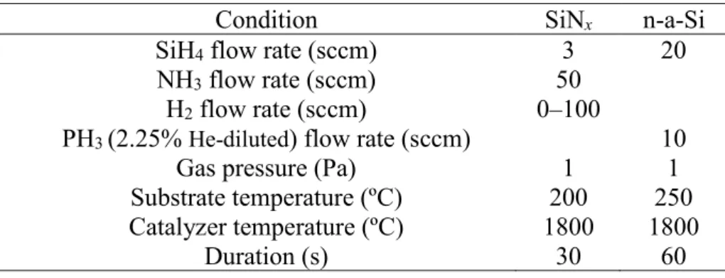
For the passivation of c-Si surfaces, SiNx films were deposited for 30 s under the
conditions shown in Table II on the both sides of Si wafers, in which H2 flow rate is
systematically changed and the refractive index and thickness of SiNx films were varied as
a result. We then deposited ~8-nm-thick n-type amorphous Si (n-a-Si) films by Cat-CVD25– 26) on the SiN
x films. The deposition condition of n-a-Si films is also summarized in Table
II. We also fabricated similar passivation structures with n-a-Si films with various thicknesses.
To improve the passivation quality of the thin SiNx films, atomic hydrogen treatment was
performed in the Cat-CVD chamber on the SiNx films prior to the deposition of n-type a-Si
films. The atomic hydrogen treatment was performed at a H2 flow rate of 20 sccm, at a
pressure of 0.2 Pa, and at substrate and catalyzer temperatures of 200 and 1800 °C, respectively.
We measured the thickness and refractive index of SiNx films by analyzing the data of
spectroscopic ellipsometry using the Cauchy model. The passivation quality of SiNx films
was characterized by measuring effective minority carrier lifetime (τeff) by microwave
photoconductivity decay (μ-PCD; KOBELCO LTA-1510 EP) using a microwave with a frequency of 10 GHz and a pulse laser with a wavelength of 904 nm and a photon density of 5×1013 cm−2.
3. Results and discussion
3.1 Passivation quality of SiNx films with different thickness
Figure 1 shows the thickness of SiNx films as a function of the duration of SiNx deposition
deposition duration, and SiNx films with thicknesses <10 nm can be obtained if we choose
deposition durations of <1 min. Figure 2 shows the τeff of the samples as a function of SiNx
thickness. We can see high τeff of ≳1 ms obtained in the samples with >15-nm-thick SiNx
films. The effective tunneling of majority carriers is, however, not expected in such thick SiNx films, and comparable τeff should be realized using much thinner SiNx films for actual
solar cells. The c-Si samples passivated with SiNx films with a thickness of less than 10 nm,
on the contrary, show drastically lower τeff. There may be two possible reasons for the
significant difference in τeff between the thick and thin SiNx samples. The first one is the
difference of the quality of the SiNx film at the film/c-Si interface. There might be a ~1-2 nm
thick SiON film near the interface, which has a fixed charge density on the order of ~1011 cm-2.27) This is lower than the value of ~1012 cm-2 for SiNx,28) and field-effect passivation
may be less effective. The second possible reason is that thicker SiNx films may be able to
keep H atoms more effectively during their deposition, which can enhance the termination of dangling bonds on the c-Si surface.
3.2 Hydrogen treatment towards thin SiNx films
To improve the passivation quality of thin SiNx films,atomic hydrogen treatment was
performed. Figure 3 shows the τeff of the c-Si samples with <5-nm-thick SiNx films deposited
at a H2 flow rate of 40 sccm as a function of atomic hydrogen treatment duration. τeff can be
improved up to >300 μs by the atomic hydrogen treatment for ~3 min. We believe that hydrogen atoms supplied during the treatment may pass through the thin SiNx films and
terminate Si dangling bonds on c-Si surfaces. The thicknesses of SiNx films measured by
spectroscopic ellipsometry were 4.45, 4.65, and 4.68 nm for atomic hydrogen treatment durations of 0, 3, and 5 min, respectively. We confirmed that there is no reduction in the thickness of SiNx films during the hydrogen treatment, showing that the SiNx films are
resistive against atomic hydrogen etching.
3.3 Hydrogen treatment towards thin SiNx films with various H2 flow rates
The atomic hydrogen treatment shows an effective improvement in τeff for the SiNx films
deposited at H2 40 sccm and a refractive index of 2.3. The effectiveness of atomic hydrogen
performed atomic hydrogen treatment towards SiNx films deposited at different H2 flow rates
as summarized in Table II.
3.3.1 Variation of the refractive index of SiNx films depending on H2 flow rate
Si/N ratio in SiNx films, to some extent, affects their refractive index.29,30) We varied H2
flow rate during the deposition of SiNx films to change their refractive index. Figure 4 shows
the thickness and refractive index of SiNx films as a function of H2 flow rate during SiNx
deposition. With increasing H2 flow rate from 0 to 100 sccm, the thickness changes slightly
from ~6 to ~4 nm, while refractive index decrease in a wide range from ~2.9 to ~2.0 at a wavelength of 640 nm. The decrease in SiNx thickness by increasing H2 flow rate may be
due to decrease in the partial pressures of SiH4 and NH3. The reason for the decrease in
refractive index is the enhancement of the decomposition of NH3 molecules through
vapor-phase reaction with hydrogen atoms—NH3 +H NH2 + H2.31)
3.3.2 τeff variation of c-Si with thin SiNx films after atomic hydrogen treatment
Based on the variation of the refractive index of SiNx films shown in Fig. 4, we prepared
the samples with different SiNx films deposited at H2 flow rates from 0 to 80 sccm for τeff
measurement. We obtained SiNx films with refractive indices of 2.1–2.9. Atomic hydrogen
treatment was then performed in the Cat-CVD chamber prior to the deposition of n-type a-Si films.
Figure 5 shows the τeff of the c-Si samples passivated with ~5-nm-thick SiNx films with
different refractive indices as a function of atomic hydrogen treatment duration. The c-Si samples passivated with highly Si-rich SiNx films, with a refractive index of ~2.9, do not
gain any τeff improvement by atomic hydrogen treatment. On the contrary, the τeff of the other
samples passivated with SiNx films with lower refractive indices can be significantly
improved, and the τeff tends to saturate with increase in atomic hydrogen treatment duration.
The τeff of the c-Si samples passivated with SiNx films with refractive indices of 2.1 and 2.2
is particularly improved up to >400 μs (~800 μs as the maximum values) by atomic hydrogen treatment. The τeff improvement is saturated at a treatment duration of ~4 min. The samples
with SiNx with a refractive index of 2.3 show lower maximum τeff and shorter hydrogen
atomic hydrogen treatment on τeff improvement strongly depends on the refractive index of
SiNx films. The reason for the different degree of the effect of the atomic hydrogen treatment
might be due to the difference of hydrogen desorption depending on the composition of SiNx.
SiNx films with more Si content, in general, releases hydrogen more easily,32) and hydrogen
atoms supplied by the hydrogen treatment may be released more frequently. This might also explain the difference of optimum hydrogen treat duration for τeff improvement. We have
also confirmed no reduction in the thickness of SiNx films with refractive indices of 2.1 and
2.2 by the hydrogen treatment, meaning that these SiNx films are resistive against hydrogen
etching.
3.4 Influence of the thickness of n-a-Si layers on τeff
The passivation quality of the n-a-Si/SiNx stacks may depend also on the properties of
n-a-Si films since the existence of the n-type layer induces downward band bending which leads to a decrease in the density of minority carriers near the SiNx/c-Si interfaces. We thus
also investigated the influence of the thickness of n-a-Si films on the quality of the passivation structures. We just change the duration of n-a-Si deposition in Table II. Based on the result shown in Fig. 5, we used SiNx films with a refractive index of 2.2 receiving atomic
Hydrogen treatments for 240 s.
Figure 6 shows the τeff of the c-Si samples passivated with ~5-nm-thick SiNx films as a
function of n-a-Si thickness. The c-Si samples show τeff improvement by increasing the
thickness of n-a-Si, and τeff reaches as high as >1 ms in a number of the samples when we
use n-a-Si films with thicknesses of ~10 nm. The τeff of the c-Si samples tends to be saturated
with further increase in the thickness of n-a-Si films. The increase in τeff by using thicker
n-a-Si films can be understood as more effective downward band bending. Note that we have observed much lower τeff (<150 µs) in the structures without SiNx layers.
In this study, we have clarified the importance of the composition of SiNx films and the
thickness of n-a-Si films to realize sufficiently high passivation ability by using the ultra-thin Cat-CVD SiNx films for the passivation of c-Si surfaces. The highest τeff obtained in this
study is comparable to that for the TOPCon structures.33) The ultra-thin SiN
x films with a
refractive index of 2.1–2.2 and high passivation ability will be applied to the rear-side passivation layers in the TOPCon-like solar cells.
4. Conclusions
We have demonstrated the effectiveness of the passivation of c-Si surfaces with ultra-thin Cat-CVD SiNx films with a thickness of <5 nm. Drastic reduction in τeff occurs by reducing
the thickness of SiNx films. However, the passivation quality of the ultra-thin SiNx films can
be significantly improved by atomic hydrogen treatment after SiNx deposition. The τeff of the
c-Si samples with SiNx with refractive indices of 2.1 and 2.2 shows particularly large
improvement in τeff up to ~800 μs by the atomic hydrogen treatment. We also confirmed that
there is no hydrogen etching of the SiNx films during the hydrogen treatment. The τeff of the
c-Si samples reach as high as >1 ms by optimizing the thickness of n-a-Si films. The ultra-thin Cat-CVD SiNx films are thus applicable to the rear contact passivation for TOPCon-like
References
1) Renewable Electricity: Insights for the Coming Decade
[https://www.nrel.gov/docs/fy15osti/63604.pdf]
2) S. S. Martin and A. Chebak, Int. J. Hydrog. Energy 41, 21036 (2016).
3) 2014 Renewable Energy Data Book [https://www.nrel.gov/docs/fy16osti/64720.pdf]
4) E. Płaczek-Popko, Opto-Electron. Rev. 25, 55 (2017).
5) J. Zhao, A. Wang, P. Altermatt, and M. A. Green, Appl. Phys. Lett. 66, 3636 (1995). 6) L. Wang, A. Lochtefeld, J. Han, A. P. Gerger, M. Carroll, J. Ji, A. Lennon, H. Li, R.
Opila, and A. Barnett, IEEE J. Photovoltaics 4, 1397 (2014).
7) H. Steinkemper, F. Feldmann, M. Bivour, and M. Hermle, IEEE J. Photovoltaics 5, 1348 (2015).
8) S. W. Glunz, F. Feldmann, A. Richter, M. Bivour, C. Reichel, H. Steinkemper, J. Benick, and M. Hermle, Proc. 31st European Photovoltaic Solar Energy Conf., 2015, p. 259.
9) S. Richter, K. Kaufmann, V. Naumann, M. Werner, A. Graff, S. Großer, A. Moldovan,
M. Zimmer, J. Rentsch, J. Bagdahn, and C. Hagendorf, Sol. Energy Mater. Sol. Cells
142, 128 (2015).
10) F. Feldmann, M. Simon, M. Bivour, C. Reichel, M. Hermle, and S. W. Glunz, Sol. Energy Mater. Sol. Cells 120, 270 (2014).
11) Y. Tao, V. Upadhyaya, K. Jones, and A. Rohatgi, AIMS Mater. Sci. 3, 180 (2016). 12) A. Moldovan, F. Feldmann, M. Zimmer, J. Rentsch, J. Benick, and M. Hermle, Sol.
Energy Mater. Sol. Cells 142, 123 (2015).
13) I. Kobayashi, T. Ogawa, and S. Hotta, Jpn. J. Appl. Phys. 31, 336 (1992).
14) S. Miyazaki, M. Narasaki, A. Suyama, M. Yamaoka, and H. Murakami, Appl. Surf. Sci.
216, 252 (2003).
15) W. C. Lee and C. M. Hu, IEEE Trans. Electron Devices 48, 1366 (2001).
16) H. Matsumura, Jpn. J. Appl. Phys. 25, L949 (1986).
17) H. Matsumura and H. Tachibana, Appl. Phys. Lett. 47, 833 (1985).
18) K. Koyama, K. Ohdaira, and H. Matsumura, Thin Solid Films 519, 4473 (2011).
19) K. Koyama, K. Ohdaira, and H. Matsumura, Appl. Phys. Lett., 97, 082108(2010)
20) T. C. Thi, K. Koyama, K. Ohdaira, and H. Matsumura, J. Appl. Phys. 116, 044510 (2014).
(2016).
22) T. C. Thi, K. Koyama, K. Ohdaira, and H. Matsumura, Jpn. J. Appl. Phys. 53, 022301
(2014).
23) T. Oikawa, K. Ohdaira, K. Higashimine, and H. Matsumura, Curr. Appl. Phys. 15, 1168
(2015).
24) K. Ohdaira, T. C. Thi, and H. Matsumura, Jpn. J. Appl. Phys. 56, 102301 (2017).
25) S. Nishizaki, K. Ohdaira, and H. Matsumura Thin Solid Films 517, 3581 (2009).
26) T. Hayakawa, M. Miyamoto, K. Koyama, K. Ohdaira, H. Matsumura, Thin Solid Films
519, 4466 (2011).
27) R. Schorner and R. Hezel, IEEE Trans. Electron Devices 28, 1466(1981)
28) A. G. Aberle, Sol. Energy Mater. Sol. Cells 65, 239(2001)
29) P. V. Bulkin, P. L. Swart, and B. M. Lacquet, Thin Solid Films 241, 247 (1994). 30) G. Xu, P. Jin, M. Tazawa, and K. Yoshimura, Thin Solid Films 425, 196 (2003).
31) H. Umemoto, K. Ohara, D. Morita, T. Morimoto, M. Yamawaki, A. Masuda, and H. Matsumura, Jpn. J. Appl. Phys. 42, 5315 (2003).
32) J. -F. Lelièvre, E. Fourmond, A. Kaminski, O. Palais, D. Ballutaud, and M. Lemiti, Sol. Energy Mater. Sol. Cells 93, 1281 (2009).
33) F. Feldmann, M. Bivour, C. Reichel, H. Steinkemper, M. Hermle, S. W. Glunz, Sol. Energy Mater. Sol. Cells 131, 46 (2014).
Table I. Deposition conditions of SiNx films for the experiment to obtain thin SiNx films.
Condition Value
SiH4 flow rate (sccm)
NH3 flow rate (sccm)
H2 flow rate (sccm)
Gas pressure (Pa) Substrate temperature (ºC) Catalyzer temperature (ºC) Duration (s) 3 50 40 1 200 1800 30–420
Table II. Deposition conditions of SiNx films for the passivation of c-Si surfaces.
Condition SiNx n-a-Si
SiH4 flow rate (sccm)
NH3 flow rate (sccm)
H2 flow rate (sccm)
PH3 (2.25% He-diluted) flow rate (sccm)
Gas pressure (Pa) Substrate temperature (ºC) Catalyzer temperature (ºC) Duration (s) 3 50 0–100 1 200 1800 30 20 10 1 250 1800 60
Figure Captions
Fig. 1. (Color online) Thickness of SiNx films as a function of deposition duration.
Fig. 2. (Color online) τeff of the samples with SiNx layers as a function of the thickness of
SiNx layers.
Fig. 3. (Color online) τeff of the samples with SiNx layers as a function of the duration of
atomic hydrogen treatment.
Fig. 4. (Color online) Thickness and refractive index of SiNx layers as a function of H2 flow
rate during SiNx deposition.
Fig. 5. (Color online) τeff of the samples passivated with SiNx layers with different refractive
index as a function of the duration of atomic hydrogen treatment.
Fig. 6. (Color online) τeff of the samples passivated with SiNx layers receiving atomic
(Color online) Figure 1.
40
30
20
10
0
T
h
ic
k
n
es
s
(n
m
)
8
7
6
5
4
3
2
1
0
Duration (min)
(Color online) Figure 2.
1600
1400
1200
1000
800
600
400
200
0
L
if
et
im
e
(µ
s)
40
35
30
25
20
15
10
5
0
Thickness (nm)
refractive index ~2.3
(Color online) Figure 3.
400
300
200
100
0
L
if
et
im
e
(µ
s)
300
250
200
150
100
50
0
Duration (s)
refractive index ~2.3
(Color online) Figure 4. 7 6 5 4 3 2 1 0
T
h
ic
k
n
es
s
(n
m
)
100 80 60 40 20 0H
2flow rate (sccm)
3.0 2.8 2.6 2.4 2.2 2.0 1.8R
ef
ra
ct
iv
e
in
d
ex
Thickness Refractive index(Color online) Figure 5. 900 800 700 600 500 400 300 200 100 0 L if e ti m e (µ s) 280 240 200 160 120 80 40 0 Duration (s) n ~2.9 n ~2.5 n ~2.3 n ~2.2 n ~2.1
(Color online) Figure 6. 1400 1200 1000 800 600 400 200 0