Fundamental Study on Designed Synthesis of Single Crystalline Metal Oxide Nanowires by A Vapor-Liquid-Solid Process
朱, 澤涛
http://hdl.handle.net/2324/2236278
出版情報:九州大学, 2018, 博士(工学), 課程博士 バージョン:
権利関係:
Single Crystalline Metal Oxide Nanowires by A Vapor-Liquid-Solid Process
気液固成長プロセスを介した単結晶金属酸化物ナノ ワイヤの構造 ・ 機能設計に関する基礎的研究
ZHU ZETAO
PH.D THESIS MARCH 2019
Fundamental Study on Designed Synthesis of Single Crystalline Metal Oxide Nanowires by
A Vapor-Liquid-Solid Process
A DISSERTATION SUBMITTED TO
INTERDISCIPLINARY GRADUATE SCHOOL OF ENGINEERING SCIENCE,
KYUSHU UNIVERSITY
IN PARTIAL FULFILLMENT OF REQUIREMENTS FOR THE DEGREE OF
DOCTOR OF PHILOSOPHY IN ENGINEERING
ZHU ZETAO
March 2019
i
ABSTRACT
This thesis has been devoted to fundamental study on designed synthesis of single crystalline metal oxide nanowires by a vapor-liquid-solid (VLS) process. This kind of nanowires attract much attention due to their unique physical properties and various applications. However, the species of functional metal oxide nanowires formed by VLS method are limited without understanding the underlying growth mechanism although the oxide system must be more complex due to its multi- element system. Furthermore, the VLS process of metal oxides in general requires relatively high growth temperatures. In addition, as semiconductors, wide range control of carrier density has played an essential role on developments of devices. Such wide range control of carrier density of oxide nanowires has been impossible due to the occurrence of unintentional carrier doping. These problems of oxide nanowires would essentially limit the wide range of its applications. This study aims to solve the problems mentioned above. The details are shown as follows;
Firstly, we show a strategy to firstly fabricate single crystalline NiO nanowires via VLS route, which essentially expands the material species of novel oxide nanowires via VLS process. Our strategy is based on the suppression of the nucleation at vapor-solid (VS) interface, which promotes the nucleation only at liquid-solid (LS) interface. Furthermore, this strategy allows us to reduce the growth temperature of single crystalline NiO nanowires, which is the lowest growth temperature so far reported.
Secondly, we propose a rational concept to reduce the growth temperature in VLS growth process of various metal oxide nanowires. Molecular dynamics (MD) simulation theoretically predicts that it is possible to reduce the growth temperature in VLS process of metal oxide nanowires by precisely controlling the vapor flux. Experimentally, we found the applicability of this concept for reducing the growth temperature of VLS processes for various metal oxides including MgO, SnO2 and ZnO. In addition, we show the successful applications of this concept to VLS nanowire growths of metal oxides onto tin-doped indium oxide (ITO) glass and polyimide (PI) substrates, which require relatively low growth temperatures.
Finally, we demonstrate 6 orders of magnitude control of electrical conductivity of single crystalline Sb-doped SnO2 nanowires grown via VLS process with the spatial homogeneity of dopants. This electrical conductivity range via an intentional impurity doping is the widest of the ones in metal oxide semiconducting nanowires reported so far. Strictly tailoring two crystal growth interfaces (LS and VS) via a flux control is required to suppress an unintentional carrier doping during a crystal growth in the presence of impurity dopants. This is because an unintentional carrier doping occurs at VS interface, controlling a crystal growth only at LS interface is essential to promote an intentional impurity doping at LS interface. In addition, the presence of Sb dopants strongly enhances a SnO2 crystal growth at VS interface, which requires further strict flux controls to suppress a detrimental unintentional carrier doping, as theoretically revealed by molecular dynamics simulations. This wide range electrical controllability of single crystalline metal oxide nanowires will be a foundation to design various electronic and energy device applications utilizing their semiconducting properties.
ii
ACKNOWLEDGEMENT
First and foremost, I wish to express my sincere gratitude to Prof. Takeshi Yanagida of Institute for Materials Chemistry and Engineering, Kyushu University for his continuous encouragement, supports and stimulating discussions. His sophisticated and exquisite viewpoints always led me to be one-step ahead. Then, I deeply express my gratitude to Prof. Kazuki Nagashima for his lots of encouragements, supports, invaluable discussions and constructive suggestions. I learned the scientific knowledge, the experimental procedures, the perspectives and the interests of research from him. I also wish to express Prof. Tsunaki Takahashi for his encouragement and kind supports.
I wish to thank Dr. Masaki Kanai for the scientific discussions and suggestions. I really thanks to Dr. Gang Meng (Professor now in Hefei Institutes of Physical Science, Chinese Academy of Sciences), Dr. Yong He (Professor now in Chongqing University) and Dr. Fuwei Zhuge (Associate Professor now in Huazhong University of Science and Technology) for their encouragements, supports, discussions and suggestions. I also wish to thank Dr. Masaru Suzuki for his Molecular Dynamics simulations based on the nanowire growth mechanism. His collective input has increased my understanding of nanowire synthesis. Then I would like to thank Dr. Guozhu Zhang and Dr. Takuro Hosomi for their kind suggestions on the experiments and scientific discussions.
In additions, I would like to thank Ms. Hiroki Imaizumi and all members in the Yanagida- Nagashima Lab. in Interdisciplinary Graduate School of Engineering Sciences. They sometimes were good rivals and were good supporters on other occasions. Also I thank Prof. Yanagida and Japan Society for the Promotion of Science for funding and supporting my study. It should be note that I would like to thank my parents for the financial and moral supports. And also I would like to thank my wife and my son for the understanding of my study and moral supports. Finally, I thank the all encounters with the kind people during my Ph. D course.
iii
CONTENTS
ABSTRACT ______________________________________________________
iACKNOWLEDGEMENT __________________________________________
iiCONTENTS ____________________________________________________
iiiCHAPTER I GENERAL INTRODUCTION __________________________
1 1.1 General Introduction ____________________________________________________ 2 1.1.1 Importance of nanowires on physical and device applications _________________ 2 1.1.2 Novelty of Metal Oxide Nanowires in VLS Process __________________________ 3 1.1.3 Impurity Doping of Metal Oxide Nanowires _______________________________ 4 1.2 Framework for Thesis ____________________________________________________ 5 1.3 References _____________________________________________________________ 7CHAPTER II LITERATE REVIEWS _______________________________
11 2.1 Introduction to metal oxide nanowires _____________________________________ 12 2.2 Synthesis and formation mechanism of metal oxide nanowires _________________ 14 2.2.1. Solution-phase growth _______________________________________________ 15 2.2.2 Vapor-phase growth__________________________________________________ 20 2.3 Current status of VLS growth mechanism in oxide nanowires 28 2.4 Doping of metal oxide nanowires __________________________________________ 31 2.5 Devices applications using metal oxide nanowires ____________________________ 34 2.5.1 Field effect transistor (FET) ___________________________________________ 34 2.5.2 Optoelectronics _____________________________________________________ 36 2.5.3 Solar cell___________________________________________________________ 40 2.5.4 Chemical sensor _____________________________________________________ 41 2.6 Summary of literate review ______________________________________________ 45 2.7 References ____________________________________________________________ 48iv
CHAPTER III TAILORING NUCLEATION AT TWO INTERFACES ENABLES SINGLE CRYSTALLINE NiO NANOWIRES VIA VAPOR-
LIQUID-SOLID _________________________________________________
65 3.1 Introduction ___________________________________________________________ 66 3.2 Experimental __________________________________________________________ 67 3.3 Result and Discussion ___________________________________________________ 69 3.4 Conclusion ____________________________________________________________ 81 3.5 References ____________________________________________________________ 82CHAPTER IV RATIONAL CONCEPT FOR REDUCING GROWTH TEMPERATURE IN VAPOR-LIQUID-SOLID PROCESS OF METAL OXIDE NANOWIRES ____________________________________________
874.1 Introduction ___________________________________________________________ 89 4.2 Experimental __________________________________________________________ 90 4.3 Result and Discussion ___________________________________________________ 94 4.4 Conclusion ___________________________________________________________ 107 4.5 References ___________________________________________________________ 108
CHAPTER V 6 ORDERS OF MAGNITUDE CONTROL OF ELECTRICAL CONDUCTIVITY OF Sb-DOPED SnO2 NANOWIRES VIA TRUE VAPOR- LIQUID-SOLID PROCESS _______________________________________
1125.1 Introduction __________________________________________________________ 114 5.2 Experimental _________________________________________________________ 116 5.3 Result and Discussion __________________________________________________ 119 5.4 Conclusion ___________________________________________________________ 131 5.5 References ___________________________________________________________ 132
CHAPTER VI OVERALL CONCLUSIONS ________________________
107LIST OF PUBLICATIONS _______________________________________
140CHAPTER I
GENERAL INTRODUCTION
2
1.1 General Introduction
1.1.1 Importance of nanowires on physical and device applications
Recently, low dimensional materials, such as 2-dimensional (2D) films, 1-dimensional (1D) nanorods and nanowires, and 0-dimensional (0D) nanoparticles and quantum dots have attracted much attention of researchers due to not only physics in mesoscale but also the emerging novel nanodevice applications[1]. Nanowires, as a significant component of 1D nanomaterials, have become the focus of intensive research owning to their unique properties in mesoscopic physics and fabrication of nanoscale devices[2]–[6]. When the diameter of a nanowire is reduced to the nanoscale domain number of atoms at the surface significantly increase along with the increase in surface area per unit volume. Hence when the diameter of nanowires decreases from micron level to nano-level the specific surface area increases by 3 orders in magnitude[7]. In such a case, the large proportions of atoms will be at or near the surface[8]. The increasing of the surface area will induce the high density of electronic states[9], which will undoubtedly affect their optical and/or electrical properties compared to the corresponding bulk materials[10],[11]. In general, nanowires provide a good system to investigate the dependence of electrical, thermal transport and mechanical properties on dimensionality (3-dimensional bulk, 2-dimensional ultra-thin film) and size (diameter) reduction, and the directionality (radial and axial)[12]. They are also suitable for fabricating the individual nanowire-based device, which play a crucial role in clarifying the electronic, optoelectronic, electrochemical and electromechanical properties with nanoscale dimensions[12]. Therefore, nanowires have been shown to provide a promising framework for nanoscience investigations and nanotechnology applications.
3
1.1.2 Novelty of metal oxide nanowires in VLS process
A variety of inorganic nanowire, including single element and compound semiconductors, have been successfully synthesized[13]–[15]. Among the semiconductors, metal oxides stand out as one of the most versatile materials, owing to their diverse properties and functionalities[16]–[18]. This is because an ionicity of semiconducting metal oxides intrinsically exhibits various unique physical properties, which are hardly attainable to conventional covalent semiconductors including Si and compounds[19]. Metal oxide nanowires not only inherit the fascinating properties from their bulk form such as piezoelectricity, chemical sensing, and photodetection, but also possess unique properties associated with their highly anisotropic geometry and size confinement[20]–
[22]. Among various crystal growth methods of semiconducting metal oxide nanowires, a vapor- liquid-solid (VLS) growth is one of most popular methods[15],[23]. This is because the VLS method offers not only a controllability of a nanowire diameter only at desired spatial position by using a catalyst droplet but also a creation of heterostructures designed within nanowires via sequentially performing a nanowire growth for different materials, which are hardly attainable to other nanowire growth methods[24],[25]. However, when compared with conventional liquid methods including hydrothermal nanowire synthesis, the growth temperature range of VLS process is relatively high compared to solution growth method[24]. Typically, the growth temperatures of VLS growth of metal oxides were ranged from 600 oC to 1000 oC[26]–[28]. This high temperature operation frequently limits the application range of VLS method, such as flexible and transparent electronics[24]. Thus, a strategy to reduce the growth temperature is desired for the VLS nanowire growth of metal oxides, which can open up opportunities to investigate the novel device applications.
4
1.1.3 Impurity doping of metal oxide nanowires
As mentioned above, semiconducting nanowires possess high potential for various device applications[29]–[31]. As semiconductors, controlling a carrier density of materials is one of the central issues to design the device specifications[32],[33]. An impurity doping enables such carrier density control of semiconductors for a wide range, which in effect has contributed to rapid developments of advanced semiconductor devices[34]–[36]. Despite these advances, many challenges remain in both understanding and controlling the doping of nanowires. The size of nanowires prevents the use of standard Hall measurements to determine doping levels, and the evaluation of carrier concentrations and mobilities remains difficult[37]. Since the dynamics of nanowire growth in VLS process is complex (such as two competing crystal growth interfaces), a serious issue of spatial inhomogeneity of dopant distribution always occurs[38]. In addition, the uncontrollable electrical conductivity has been a serious issue for practical electronic application of semiconducting metal oxide nanowires. This is because previously reported semiconducting metal oxide nanowires are highly conductive even without any intentional carrier doping[39]–[41].
This unintentional carrier doping essentially hinders the carrier density control of semiconducting metal oxide nanowires for a wide range even in the presence of impurity doping[42]. Therefore, these backgrounds motivate me to investigate the physical mechanisms of impurity doping of metal oxide nanowires in VLS process. Considering all of the above backgrounds, the main objectives of this study are:
1. To design novel oxide nanowire synthesis via VLS route by clarifying the fundamental mechanism of VLS growth.
2. To reduce growth temperature of VLS growth metal oxide nanowires by utilizing the fundamental mechanism of nanowire growth.
5
3. To control the electrical conductivity of semiconducting metal oxide nanowires by tailoring the crystal growth during VLS growth.
1.2 Framework for Thesis
This thesis is divides into six chapters. The first chapter presents a general introduction and the framework of this thesis. In chapter II, a literature review is described to give the general details of semiconducting metal oxide nanowires in VLS process and to clarify the advantages and the lack of knowledge. Since the growth of material species of metal oxide nanowires is limited by VLS process, Chapter III describes a strategy to firstly fabricate the novel functional metal oxide nanowire via VLS process by clarifying the fundamental growth mechanism of metal oxide nanowires via the VLS growth process. In this section, we show a rational strategy to firstly fabricate single crystalline NiO nanowires via VLS route, which essentially allows us to tailor the diameter and the spatial position. Our strategy is based on the suppression of the nucleation at vapor-solid (VS) interface, which promotes the nucleation only at liquid-solid (LS) interface.
Manipulating both the supplied material fluxes (oxygen and metal) and the growth temperature enables to enhance the nucleation only at LS interface. As we mentioned above, the growth temperature of VLS method is very high (Typically 600-1000 oC) compared to solution growth methods (lower than 300 oC). Chapter IV demonstrates a rational concept to reduce the growth temperature in VLS growth process of various metal oxide nanowires. Molecular dynamics (MD) simulation theoretically predicts that it is possible to reduce the growth temperature in VLS process of metal oxide nanowires by precisely controlling the vapor flux. Experimentally, we found the applicability of this concept for reducing the growth temperature of VLS processes for various metal oxides including MgO, SnO2 and ZnO. In addition, we show the successful applications of this concept to VLS nanowire growths of metal oxides onto tin-doped indium oxide (ITO) glass
6
and polyimide (PI) substrates, which require relatively low growth temperatures. As semiconductors of metal oxide nanowires, control of carrier density is one of the central issue, which is not achieved so far. Chapter V describes a precisely control of a carrier density of semiconducting metal oxide nanowires by impurity doping, which is one of the central issues to design the device specifications. In this part, 6 orders of magnitude control of electrical conductivity of single crystalline Sb-doped SnO2 nanowires grown via vapor-liquid-solid (VLS) process with the spatial homogeneity of dopants is achieved. This electrical conductivity range via an intentional impurity doping is the widest of the ones in metal oxide semiconducting nanowires reported so far. Strictly tailoring two crystal growth interfaces (LS and VS) via a flux control is required to suppress an unintentional carrier doping during a crystal growth in the presence of impurity dopants. This is because an unintentional carrier doping occurs at VS interface, controlling a crystal growth only at LS interface is essential to promote an intentional impurity doping at LS interface. In addition, the impact of impurity dopants on the crystal growth of nanowires in VLS process is clarified and theoretically revealed by MD simulations. The last Chapter summarizes the all results and conclusions in this thesis.
7
1.3 References
[1] Thelander, C.; Agarwal, P.; Brongersma, S.; Eymery, J.; Feiner, L. F.; Forchel, A.; Scheffler, M.; Riess, W.; Ohlsson, B. J.; Gösele, U.; Samuelson, L. Nanowire-based one-dimensional electronics. Mater. Today 2006,9, 28-35.
[2] Lu, W.; Lieber, C. M. Semiconductor nanowires. J. Phys. D: Appl. Phys. 2006,39, 387.
[3] Huang, M. H.; Mao, S.; Feick, H.; Yan, H.; Wu, Y.; Kind, H.; Weber, E.; Russo, R.; Yang, P.
Room-temperature ultraviolet nanowire nanolasers. Science 2001, 292, 1897-1899.
[4] Cui, Y.; Lieber, C. M. Functional nanoscale electronic devices assembled using silicon nanowire building blocks. Science 2001, 291, 851-853.
[5] Hochbaum, A. I.; Yang, P. Semiconductor nanowires for energy conversion. Chem. Rev. 2010, 110, 527-546.
[6] Hochbaum, A. I.; Chen, R.; Delgado, R. D.; Liang, W.; Garnett, E. C.; Najarian, M.; Majumdar, A.; Yang, P. Enhanced thermoelectric performance of rough silicon nanowires. Nature 2008, 451, 163.
[7] Kuchibhatla, S. V. N. T.A.; Karakoti, S.; Bera, D.; Seal, S. One dimensional nanostructured materials. Prog. Mater. Sci. 2007, 52, 699-913.
[8] Suryanarayana, C. Recent developments in nanostructured materials. Adv. Eng. Mater. 2005, 7, 983-992.
[9] Himpsel, F. J.; Altmann, K. N.; Bennewitz, R.; Crain, J. N.; Kirakosian, A.; Lin, J. L.;
McChesney, J. L. One-dimensional electronic states at surfaces. J. Phys. Condens. Matter 2001, 13, 11097.
[10] Liao, Z. M.; Liu, K. J.; Zhang, J. M.; Xu, J.; Yu, D. P. Effect of surface states on electron transport in individual ZnO nanowires. Phys. Lett. A 2007, 367, 207-210.
[11] Halpern, E.; Elias, G.; Kretinin, A. V.; Shtrikman, H.; Rosenwaks, Y. Direct measurement of surface states density and energy distribution in individual InAs nanowires. Appl. Phys. Lett.
2012, 100, 2621095.
[12] Xia, Y.; Yang, P.; Sun, Y.; Wu, Y. One‐dimensional nanostructures: synthesis, characterization, and applications. Adv. mater. 2003, 15, 353-389.
[13] Hochbaum, A. I.; Fan, R.; He, R.; Yang, P. Controlled growth of Si nanowire arrays for device integration. Nano Lett., 2005, 5, 457-460.
[14] Hersee, S. D.; Sun, X.; Wang, X. The controlled growth of GaN nanowires. Nano Lett. 2006,
8 6, 1808-1811.
[15] Klamchuen, A.; Suzuki, M.; Nagashima, K.; Yoshida, H.; Kanai, M.; Zhuge, F.; He, Y.; Meng, G.; Kai, S.; Takeda, S.; Kawai, T.; Yanagida, T. Rational Concept for Designing Vapor-Liquid- Solid Growth of Single Crystalline Metal Oxide Nanowires. Nano Lett. 2015, 15, 6406-6412.
[16] Shen, G.; Chen, P. C.; Ryu, K.; Zhou, C. Devices and chemical sensing applications of metal oxide nanowires. J. Mater. Chem. 2009, 7, 828-839.
[17] Wang, X.; Song, J.; Liu, J.; Zhong, L. W. Direct-current nanogenerator driven by ultrasonic waves. Science 2007, 316, 102-105.
[18] Su, J.; Feng, X.; Sloppy, J. D.; Guo, L.; Grimes, C. A. Vertically aligned WO3 nanowire arrays grown directly on transparent conducting oxide coated glass: Synthesis and photoelectrochemical properties. Nano Lett. 2011, 11, 203-208.
[19] Pan, Z. W.; Dai, Z. R.; Wang, Z. L. Nanobelts of semiconducting oxides. Science 2001, 291, 1947-1949.
[20] Wang Z. L.; Song, J. Piezoelectric nanogenerators based on zinc oxide nanowire arrays.
Science 2006, 312, 242-246.
[21] Zhang, D.; Liu, Z.; Li, C.; Tang, T.; Liu, X.; Han, S.; Lei, B.; Zhou, C. Detection of NO2
down to ppb levels using individual and multiple In2O3 nanowire devices. Nano Lett. 2004, 4, 1919-1924.
[22] Irvin, P.; Ma, Y.; Bogorin, D. F.; Cen, C.; Bark, C. W.; Folkman, C. M.; Eom, C. B.; Levy, J.
Rewritable nanoscale oxide photodetector. Nat. Photonics, 2010, 4, 849.
[23] Yang, P.; Yan, H.; Mao, S.; Russo, R.; Johnson, J.; Saykally, R.; Morris, N.; Pham, J.; He, R.;
Choi, H. J. Controlled growth of ZnO nanowires and their optical properties. Adv. Funct. Mater.
2002, 12, 323-331.
[24] Zhu, Z.; Suzuki, M.; Nagashima, K.; Yoshida, H.; Kanai, M.; Meng, G.; Anzai, H.; Zhuge, F.; He, Y.; Boudot, M.; Takeda, S.; Yanagida, T. Rational concept for reducing growth temperature in vapor-liquid-solid process of metal oxide nanowires. Nano Lett. 2016, 16, 7495- 7502.
[25] Anzai, H.; Suzuki, M.; Nagashima, K.; Kanai, M.; Zhu, Z.; He, Y.; Boudot, M.; Zhang, G.;
Takahashi, T.; Kanemoto, K.; Seki, T.; Yanagida, T. True vapor–liquid–solid process suppresses unintentional carrier doping of single crystalline metal oxide nanowires. Nano Lett.
2017, 17, 4698-4705.
9
[26] Nagashima, K.; Yanagida, T.; Oka, K.; Tanaka, H.; Kawai, T.; Mechanism and control of sidewall growth and catalyst diffusion on oxide nanowire vapor-liquid-solid growth. Appl.
Phys. Lett. 2008, 93, 153103.
[27] Yanagida, T.; Nagashima, K.; Tanaka, H.; Kawai, T.; Mechanism of critical catalyst size effect on MgO nanowire growth by pulsed laser deposition. J. Appl. Phys., 2008, 104, 016101.
[28] Meng, G.; Yanagida, T.; Yoshida, H.; Nagashima, K.; Kanai, M.; Zhuge, F.; He, Y.;
Klamchuen, A.; Rahong, S.; Fang, X.; Takeda, S. A flux induced crystal phase transition in the vapor-liquid-solid growth of indium-tin oxide nanowires. Nanoscale 2014, 6, 7033-7038.
[29] Heo, Y. W.; Norton, D. P.; Tien, L. C.; Kwon, Y.; Kang, B. S.; Ren, F.; Pearton, S. J.; LaRoche, J. R. ZnO nanowire growth and devices. Mater. Sci. Eng. R: Reports 2004, 47, 1-47.
[30] Nguyen, P.; Ng, H. T.; Yamada, T.; Smith, M. K.; Li, J.; Han, J.; Meyyappan, M. Direct integration of metal oxide nanowire in vertical field-effect transistor. Nano Lett. 2004, 4, 651- 657.
[31] Xia, X.; Tu, J.; Zhang, Y.; Wang, X.; Gu, C.; Zhao, X. B.; Fan, H. J. High-quality metal oxide core/shell nanowire arrays on conductive substrates for electrochemical energy storage. ACS Nano 2012, 6, 5531-5538.
[32] Kobayashi, S.; Nishikawa, T.; Takenobu, T.; Mori, S.; Shimoda, T.; Mitani, T.; Shimotani, H.; Yoshimoto, N.; Ogawa, S.; Iwasa, Y. Control of carrier density by self-assembled monolayers in organic field-effect transistors. Nat. Mater. 2004, 3, 317.
[33] Ohtomo, A.; Hwang, H. Y. Growth mode control of the free carrier density in SrTiO3-δ films.
J. Appl. Phys. 2007, 102, 083704.
[34] Ko, H. J.; Chen, Y. F.; Hong, S. K.; Wenisch, H.; Yao, T.; Look, D. C. Ga-doped ZnO films grown on GaN templates by plasma-assisted molecular-beam epitaxy. Appl. Phys. Lett. 2000, 77, 3761-3763.
[35] Fabregat-Santiago, F.; Barea, E. M.; Bisquert, J.; Mor, G. K.; Shankar, K.; Grimes, C. A.
High carrier density and capacitance in TiO2 nanotube arrays induced by electrochemical doping. J. Am. Chem. Soc., 2008, 103, 11312-11316.
[36] Sahu, A.; Kang, M. S.; Kompch, A.; Notthoff, C.; Wills, A. W.; Deng, D.; Winterer, M.;
Frisbie, C. D.; Norris, D. J. Electronic impurity doping in CdSe nanocrystals. Nano Lett. 2012, 12, 2587-2594.
[37] Storm, K.; Halvardsson, F.; Heurlin, M.; Lindgren, D.; Gustafsson, A.; Wu, P. M.; Monemar,
10
B.; Samuelson, L. Spatially resolved Hall effect measurement in a single semiconductor nanowire. Nat. Nanotechnol. 2012, 7, 718.
[38] Klamchuen, A.; Yanagida, T.; Nagashima, K.; Seki, S.; Oka, K.; Taniguchi, M.; Kawai, T.
Crucial role of doping dynamics on transport properties of Sb-doped SnO2 nanowires. Appl.
Phys. Lett. 2009, 95, 053105.
[39] Fonstad C. G.; Rediker, R. H. Electrical properties of high-quality stannic oxide crystals. J.
Appl. Phys. 1971, 42, 2911-2918.
[40] Wan, Q.; Dattoli, E. N.; Fung, W. Y.; Guo, W.; Chen, Y.; Pan, X.; Lu, W. High-performance transparent conducting oxide nanowires. Nano Lett. 2006, 6, 2909-2915.
[41] Samson, S.; Fonstad, C. G. Defect structure and electronic donor levels in stannic oxide crystals. J. Appl. Phys. 1973, 44, 4618-4621.
[42] Guo, Z.; Chen, X.; Xu, W. H.; Li, J.; Yang, G. M.; Li, M. Q.; Liu, J. H.; Huang, X. J. T- shaped SnO2 nanowire current splitter. Mater. Today 2011, 14, 42-49.
CHAPTER II
LITERATE REVIEWS
12
2.1 Introduction to metal oxide nanowires
During the last half century, a dramatic downscaling of electronics has taken place, a miniaturization that the industry expects to continue for at least a decade[1]. Nanostructures are defined as having at least one dimension between 1 and 100 nm, have received steadily growing interests as a result of peculiar and fascinating properties, and applications superior to their bulk counterparts[2], [3]. The ability to generate such minuscule structures is essential to much of modern science and technology. There are a large amount of opportunities that might be realized by making new types of nanostructures, or simply by down-sizing existing microstructures into the 1-100 nm regime. The most successful example is provided by microelectronics, where “small”
has meant greater performance ever since the invention of integrated circuits: more components per chip, faster operation, low cost, and less power consumption[4]. Miniaturization may also represent the trend in a range of other technologies[5]. In information storage, for example, there are many active efforts to develop magnetic and optical storage component with critical dimensions as small as tens of nanometers[6]. It is also clear that a wealth of interesting and new phenomena are associated with nanometer-sized structures, with the best established examples including size-dependent excitation or emission, quantized conductance, Coulomb blockade and metal-insulator transition[7]–[11]. It is generally accepted that quantum confinement of electrons by the potential wells of nanometer-sized structures may provide one of the most powerful means to control the electrical, optical, magnetic and thermoelectric properties of a solid-state functional material[12]–[15].
Recently, nanowires have also become the focus of intensive research owing to their unique applications in mesoscopic physics and fabrication of nanoscale device[16]–[20]. It is generally accepted that nanowires provide a good system to investigate the dependence of electrical and
13
thermal transport or mechanical properties on dimensionality and size reduction[4]. They are also expected to play an important role as both interconnects and functional units in fabricating electronic, optoelectronic, electrochemical and electromechanical devices with nanoscale dimensions[21]–[24].
In the late 1990s, the field of nanowires underwent a significant expansion and became one of the most active research areas within the nanoscience and nanotechnology community[25], [26].
Exciting developments have been made from many research groups around the world in recent years, including the Lieber group[18], [27]–[31], Yang group[32]–[35], Zhou group[36]–[38], Wang group[39]–[41] and Yanagida group[42]–[45] at Kyushu university. This research field of nanowires has a promising potential for studying the fundamental nanoscience and functional applications, which can be seen from the vast number of papers published in two past decades, as shown in Figure 2.1.
Figure 2.1 Increasing of the number of published papers in the nanowire field per year from year 1995 to 2014.
A variety of inorganic nanowires, including single element and compound semiconductors, have been successfully synthesized[35], [46], [47]. With their in-depth physical property characterizations, they have demonstrated to be promising candidates for future nanoscale
14
electronic, optoelectronic and sensing device applications. Among the semiconductors, metal oxides stand out as one of the most versatile materials, owing to their diverse properties and functionalities[37], [48], [49].Their nanowire structures not only inherit the fascinating properties from their bulk form such as piezoelectricity, chemical sensing, and photodetection, but also possess unique properties associated with their highly anisotropic geometry and size confinement[50]–[52]. In details, metal oxide nanowires have several advantages with respect to their traditional thin- and thick film counterpart such as very large surface-to-volume ratio, dimensions comparable to the extension of surface charge region, superior stability owing to the high crystallinity, relatively simple preparation methods, possible functionalization of their surface with a target specific receptor species, modulation of their operating temperature to select the proper gas semiconductor reactions, catalyst deposition over the surface for promotion or inhibition of specific reactions and finally the possibility of field-effect transistors (FET) configuration[53]–[55]. Preparation and performances of these emerging metal oxide nanosized structures have been reviewed by a number of authors, but this research field is growing so fast that there is still the need of a review focusing on the designing of the nanowire.
2.2 Synthesis and formation mechanism of metal oxide nanowires
A variety of methods have been utilized to grow metal oxide nanowires. They can be divided into two different approaches of top-down and bottom-up technologies[56]. The first one is based on standard micro fabrication methods with deposition, etching and ion beam milling on planar substrates in order to reduce the lateral dimensions of the films to the nanometer size[57]–[59].
The advantages are the use of the well-developed technology of semiconductor industry and the ability to work on planar surfaces, while disadvantages are their extremely elevated costs and preparation times. In the top-down approach highly ordered nanowires can be obtained, but at the
15
moment this technology does not fulfil the industrial requirements for the production of low cost and large numbers of devices[60]–[62]. Furthermore, the nanowires produced with these techniques are in general not single-crystalline[63]. The second approach, bottom-up, consists of the assembly of molecular building blocks or chemical synthesis by vapor phase transport, electrochemical deposition, solution-based techniques or template growth[64]–[66]. Its advantages are the high purity of the produced nanocrystalline materials, the small diameters, the low cost of the experimental set ups together with the possibility to easily vary the intentional doping and the possible formation of junctions. The main disadvantage regards their integration on planar substrates for the exploitation of their useful properties, for example transfer and contacting on transducers can be troublesome. The bottom-up approach allows low cost fabrication although it could be very difficult to get them well arranged and patterned[67]. This study will be focused on the bottom-up techniques for the preparation of single crystal nanowires.
According to the synthesis environment, bottom-up techniques for nanowire growth can be mainly divided into two categories: liquid (solution) phase growth and vapor phase growth.
Solution-phase growth methods provide a flexible synthesis process and an alternative to achieve lower cost[68]. On the other hand, many metal oxide nanowires are grown via the well-developed vapor phase technique, which is based on the reaction between metal vapor and oxygen gas[69].
The governing mechanisms are the vapor–liquid–solid process (VLS) and vapor–solid process (VS)[70]. This section will present a survey of various reports on the synthesis of metal oxide nanowires using these methods.
2.2.1. Solution-phase growth
Growth of nanowires in solution phase has been successfully achieved. This growth method usually requires ambient temperature so that it considerably reduces the complexity and cost of
16
fabrication. To develop strategies that can guide and confine the growth direction to form nanowire, researchers have used a number of approaches which may be grouped into template-assisted method and template-free method.
2.2.1.1 Template-assisted synthesis
Large-area patterning of metal oxide nanowire array assisted by template has been achieved[71].
By utilizing a periodic-structured template, such as anodic aluminum oxide, molecular sieves, and polymer membranes, nanostructures can form inside the confined channels. For example, anodic aluminum oxide (AAO) membranes have embedded hexagonally ordered nanochannels. They are prepared via the anodization of pure aluminum in acidic solution[72]. These pores can be filled to form nanowire using electrodeposition and sol–gel deposition methods. Because the diameter of these nanochannels and the inter-channel distance are easily controlled by the anodization voltage, it provides a convenient way to manipulate the aspect ratio and the area density of nanowire.
2.2.1.1.1 Electrochemical deposition. Electrochemical deposition has been widely used to fabricate metallic nanowires in porous structures. It was found that it is also a convenient method to synthesize metal oxide nanostructures. In fact, there are both direct and indirect approaches to fabricate metal oxide nanowires using electrodeposition. In the direct method, by carefully choosing the electrolyte, ZnO, Fe2O3, Cu2O and NiO nanowires have been successfully synthesized[65], [73]–[75]. In an indirect approach, Chen et al. deposited tin metal into AAO by electrochemical deposition and then thermally annealed it to obtain SnO2 nanowires embedded in AAO template[76]. The general schematic for the synthesis of nanowires by deposition of materials into the AAO nanoporous templates is shown in Figure 2.2[77].
17
Figure 2.2 General schematic for the synthesis of nanowires by deposition of materials into the AAO nanoporous templates[77].
2.2.1.1.2 Sol–gel deposition. In general, sol–gel process is associated with a gel composed of sol particles. As the first step, colloidal (sol) suspension of the desired particles is prepared from the solution of precursor molecules. An AAO template will be immersed into the sol suspension, so that the sol will aggregate on the AAO template surface. With an appropriate deposition time, sol particles can fill the channels and form structures with high aspect ratio. The nanowire can be obtained by utilizing a thermal treatment to remove the gel. By utilizing the sol-gel method, ZnO nanowires were obtained by soaking AAO into zinc nitrate solution mixed with urea and kept at 80 oC followed by thermal heating[78]. Successful formation of MnO2, ZrO2, TiO2 and various multi-compound oxide nanowires was reported on the basis of similar processes[79]–[84].
The template assisted solution method shows a simple approach to fabricate the nanowires with controlled position, diameter and area density. However, since the materials fabricated by this technique is limited to metals, a second reaction is needed to transform them onto semiconductors like metal oxide nanowires. In addition, for semiconductor nanowires, the non-epitaxial growth
18
and amorphous or polycrystalline in structure are the key disadvantages for the electronic applications, because they are consisted of small crystals with an abundance of defects.
2.2.1.2 Template-free methods
Instead of plating nanomaterials inside a template, much research effort is triggered to develop new techniques to direct nanowire growth in liquid environment. The most important procedures will be described below including surfactant method, sonochemistry, and hydrothermal technique.
2.2.1.2.1 Surfactant-assisted growth. The use of a surfactant can promote the anisotropic crystal growth required for the production of one-dimensional crystals. This anisotropic growth is often carried out in a microemulsion system composed of three phases: oil phase, surfactant phase and aqueous phase. In the emulsion system, these surfactants serve as microreactors to confine the crystal growth. To obtain desired materials, one needs to prudently select the species of precursor and surfactants, and also set the other parameters such as temperature, pH value, and concentration of the reactants. Different surfactants were proposed depending on the material that is addressed, for example oleic acid, hexylphosphonic acid (HPA), tetradecylphosphonic acid (TDPA), trioctylphosphine oxide (TOPO) and trioctylphosphine (TOP). As a result, surfactant-assisted system is a trial-and-error based procedure which requires much endeavor to choose proper capping agents and reaction environment. By using this process, ZnO, SnO2, NiO nanowires had been successfully synthesized[85]–[87]. Reports on lead oxide (PbO2), chromate (PbCrO4, CuCrO4, BaCrO4), cerium oxide (CeO2) nanowires have also been published[88]–[90].
2.2.1.2.2 Sonochemical method. Sonochemical method uses ultrasonic wave to acoustically agitate or alter the reaction environment, thus modifies the crystal growth. The sonication process is based on the acoustic cavitation phenomenon which involves the formation, growth, and collapse of many bubbles in the aqueous solution[91]. Extreme reaction conditions can be created at localized
19
spots. Assisted by the extreme conditions, for example, at temperature greater than 5000 K, pressure larger than 500 atm, and cooling rate higher than 1010 K/s, nanostructures of metal oxides can be formed via chemical reactions. Kumar et al. have synthesized magnetite (Fe3O4) nanowires in early days by ultrasonically irradiating aqueous iron acetate in the presence of beta-cyclodextrin which serves as a size-stabilizer[92]. Hu et al. later demonstrated that linked ZnO wires can be fabricated by ultrasonic irradiation under ambient conditions and assisted by microwave heating[93]. Recently, nanocomposite materials have been grown by applying this technique; Gao et al. synthesized and characterized ZnO nanowire/CdS nanoparticle (core/shell) composites[94].
Nanowires of rare earth metal oxides, such as europium oxide (Eu2O3) has also been obtained via this method[95].
2.2.1.2.3 Hydrothermal. Hydrothermal process has been carried out to produce crystalline structures since the 1970s. This process begins with aqueous mixture of soluble metal salt (metal and/or metal–organic) of the precursor materials. Usually the mixed solution is placed in an autoclave under elevated temperature and relatively high-pressure conditions. Typically, the temperature ranges between 100 oC and 300 oC and the pressure exceeds 1 atm. Many works have been reported to synthesize ZnO nanowires by using wet-chemical hydrothermal approaches[96]–
[98]. Via this technique, other oxide nanowires have also been produced, such as CuO, Ga2O3, perovskite manganites (Fe3O4), CeO2, TiO2 and In2O3[99]–[105].
Thus, the solution methods without a template have several invaluable advantages such as high yield, low temperature and low cost. The key points to develop this technique are position control, growth direction control and high crystallinity. However, this method provides little control over the area density, the diameter and the nanowire have smaller aspect ratio than those grown by vapor phase technique. In addition, the nanowires exhibit poor vertical alignment.
20
2.2.2 Vapor phase growth
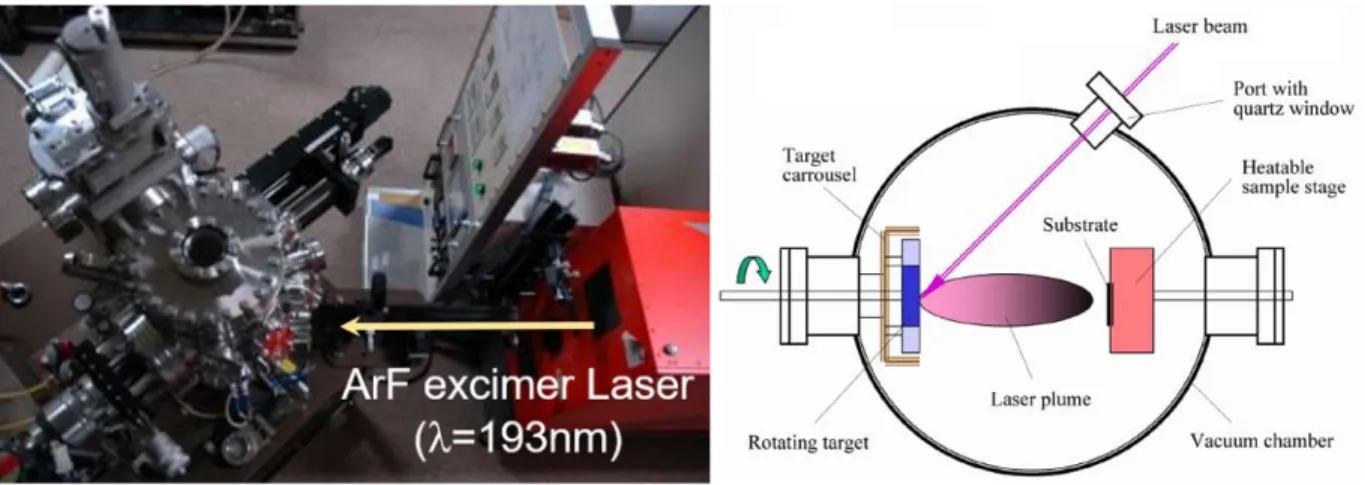
High-temperature vapor phase growth assisted by a thermal furnace is a straightforward approach that controls the reaction between metal vapor source and oxygen gas. In order to control the diameter, aspect ratio, and crystallinity, diverse techniques have been exploited including thermal chemical vapor deposition (CVD), direct thermal evaporation[106], pulsed laser deposition (PLD) [107]–[109], and metal-organic chemical vapor deposition (MOCVD)[110], [111], etc. The image and schematic of a PLD system is shown in Figure 2.3. These growth methods are based on two mechanisms: vapor-solid and vapor-liquid-solid.
Figure 2.3 Image and schematic view of a pulsed laser deposition (PLD) system.
2.2.2.1 Vapor-solid mechanism
The VS growth takes place when the nanowire crystallization originates from the direct condensation from the vapor phase without the use of a catalyst[112]. It is often called self- catalytic growth since the nanowires grow directly from vapor phases. Although VS growth mechanism is not well understood, it has already proved to a very important method to synthesize nanowires. Plausible growth mechanisms to explain VS growth are as follows: intrinsic anisotropic surfaces and defect-induced growth (screw dislocation)[113]. Another peculiar effect registered was a nanowire growth rate higher than the calculated condensation rate from the vapor phase. A
21
possible interpretation is that all the faces of the nanowire adsorb the molecules that afterwards diffuse on the principal growth surface of the wire.
Figure 2.4 a, b; TEM and SEM images of Al2O3 whisker, c; The generation mechanism of Al2O3
whiskers: deposition of O2 on molten Al layer; generation of AlOx(g); growth on the direction of [001] and the formation of Al2O3 whiskers[114].
Intrinsic anisotropic surfaces. Quite a few experimental and theoretical works have proposed that the minimization of surface free energy primarily governs the VS process[115],[116]. Under high temperature condition, source materials are vaporized and then directly condensed on the substrate placed in the low temperature region. Once the condensation process happens, the initially condensed molecules form seed crystals serving as the nucleation sites. As a result, they facilitate directional growth to minimize the surface energy. This self-catalytic growth associated with many thermodynamic parameters is a rather complicated process that needs quantitative modeling[117].
It was reported for In2O3 wires were synthesized through thermal evaporation of pure In2O3
22
powders and the effect of substrate seeding was studied for controlling density distribution and lateral dimensions of the wires. The wires exhibit uniform section, atomically sharp lateral facets, and pyramidal termination, typical of a VS growth mechanism assisted by oxidized nanocrystalline seeds.
Crystal defects. Another explanation of growth mechanism of screw dislocation is proposed to explain the significant enhancement of the crystal growth of nanowires. This classical mechanism is based on the fact that the growth of a crystal proceeds by adding atoms at the kink sites of a surface step. Kink sites always exist on the steps even at the thermal equilibrium state. Due to the advance of the kink along the surface, the crystal growth progresses perpendicularly to the surface.
In thermal equilibrium state, a perfect crystal should eventually contain no surface steps. Then, the growth of a perfect crystal depends on the nucleation of surface steps[118]. For the growth of a real crystal, however, the growth rate is much faster than that predicted for a perfect crystal because real crystals contain defects, dislocations and twins. A dislocation can terminate on a defect inside the crystal or on a surface. If a dislocation terminates on a surface and its Burgers vector has a component normal to the surface (the screw component), a step forms starting from the emerging point of the dislocation. Leading by the dislocations, steps can curve into a spiral, and the growth of crystal is largely enhanced without the need of nucleation for fresh surface steps. It has been frequently observed that screw dislocations are associated with growth of crystal in the nanowire geometries[118]. Just like that in thick wires, for example ZnO nanowire (diameter>200 nm), unidirectional growth induced by dislocations in VS growth has been observed[119]. The spiral feature at each nanowire tip is obviously due to the steps generated by a screw dislocation. In thin ZnO nanowires grown by the VS growth, however, no screw dislocation existing at the core of the nanowires have been found.
23
Even though the fabrication of various semiconductor nanowires through the VS growth have been reported, the control of the spatial arrangement of nanowires is rather difficult than following VLS growth method.
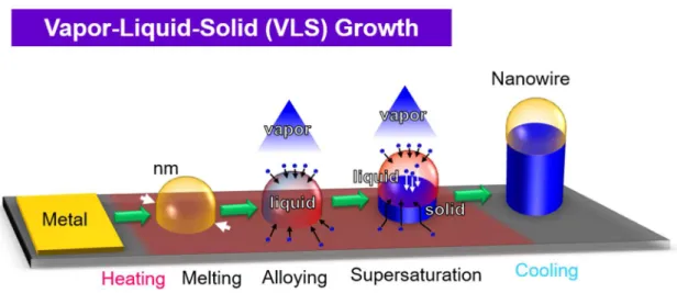
2.2.2.2 Vapor-liquid-solid mechanism
Figure 2.5 a; Binary phase diagram of Au-Si system, b; Schematic illustration of vapor-liquid- solid growth of a Si nanowire or whisker[120].
VLS mechanism was first proposed by Wagner and Ellis in 1964 while observing the growth of Si whisker[121], [122]. After that, VLS in the last decades was one of the most important methods for preparing 1D structures, it is promising as a scalable, economical and controllable growth of different materials (oxides, semiconductors). The general mechanism for VLS growth can most easily be explained by considering the binary phase diagram of the Au-Si eutectic system (Figure 2.5 a)[120],[123]. The melting temperatures of Au-Si mixtures are lower than that of the pure components with a minimum melting temperature of 363 oC occurring at 18.6 at. % Si, which is
24
referred to as the eutectic point. Consequently, when Au is heated on a Si substrate above the eutectic temperature of 363 oC, an Au-Si liquid droplet will form. When additional Si is added to the system in the form of vapor phase molecules such as SiCl4 or SiH4, the molecules will readily adsorb on the liquid surface, thereby supplying additional Si to the liquid droplet (Figure 2.5 b).
Si-containing species adsorbed on the surrounding solid surfaces can also diffuse to the liquid and become incorporated. The liquid droplet then becomes supersaturated with Si, which serves as a driving force for crystallization of the excess silicon at the liquid-solid interface. A continual supply of vapor phase Si will result in the growth of a crystalline nanowire or microwire, with the liquid droplet remaining on the tip of the wire via surface tension.
Figure 2.6 (Top) Schematic illustration of droplet and wire shape during initial stages of vapor- liquid-solid growth. (Bottom) The corresponding equilibrium balance of forces at the three phase boundary at the left edge of the droplet (dashed circle)[124].
Since Si nanowire growth occurs via crystallization from the liquid droplet, the diameter of the wire is determined by the size of the liquid droplet on the substrate surface. A model of the initial droplet shape and its evolution during wire growth was developed by Schmidt et al. [124][125].
At the initial stages of wire growth, the equilibrium shape of the liquid droplet can be described
25
by the contact angle (), which is determined by the inclination angle of the wire sidewall (α) and the balance of forces associated with the surface tension of the liquid droplet (l), the surface tension of the solid Si (s), and the interfacial tension at the liquid–solid interface (ls), as shown in Figure 2.6 where:
𝑐𝑜𝑠() = cos(𝛼) − (2.1) The inclination angle (α) is zero for the initial liquid droplet on the substrate surface, and Eqn (2.1) reduces to Young’s equation. Assuming that the droplet shape can be approximated as a segment of a sphere, the initial radius (r) at the liquid–solid interface can be described by the contact angle and the volume (V) of the droplet as: [124]
𝑟 = / ( (()) /(()) / ) / (2.2) The volume (V) of the liquid droplet can be determined from the initial radius (ro) of the liquid–
solid interface and the initial contact angle (o) as:
𝑉 = 1 − cos 2 + cos (2.3) Assuming that, during growth, there is no loss of metal from the liquid droplet due to surface diffusion or incorporation in the wire, then the droplet volume can be assumed to be constant during the entire growth process. Experimentally, it has been observed that the diameter of Si nanowires or whiskers is largest at the base near the wire substrate interface and decreases gradually over a short distance before reaching steady state as shown schematically in Figure 2.6.
The base expansion was initially explained by Weyher as arising from a change in contact angle, as the liquid droplet rose from the substrate surface due to wire growth[126]. Schmidt et al. later demonstrated that the slope of the wire sidewall near the three-phase boundary can be related to the inclination angle (α) as dh(r)/dr = -tan(α), where h is the height of the wire and r is the
26
nanowire radius. This equation can be numerically integrated to predict the shape of the nanowire (h vs r) as a function of surface tension[124].
Figure 2.7 Schematic illustrations of the growth process for a vapor-liquid-solid process.
In the case of growing metal oxide nanowires, VLS process is initiated by the formation of liquid alloy droplet which contains both catalyst and source metal. Precipitation occurs when the liquid droplet becomes supersaturated with the source metal. Under the flow of oxygen, metal oxide crystal is formed[127]. Figure 2.7 illustrates the growth processes of metal nanowires by a VLS method. Normally the resulting crystal is grown along one particular crystallographic orientation which corresponds to the minimum atomic stacking energy, leading to nanowire structure formation. Wu et al. have provided direct evidence of VLS growth by means of real time in situ transmission electron microscope observations[128]. This work depicts a vivid dynamic insight and elucidates the understanding of such microscopic chemical process. A majority of oxide nanowires has been synthesized via this catalyst-assisted mechanism, such as ZnO, MgO, CaO, NiO, TiO2, SnO2, In2O3, and Ga2O3[47], [105], [129]–[133]. Several approaches have been developed based on the VLS mechanism. As an example, thermal CVD synthesis process utilizes a thermal furnace to vaporize the metal source, then proper amount of oxygen gas is introduced
27
through mass flow controller. In fact, metal and oxygen vapor can be supplied via different ways, such as carbothermal or hydrogen reduction of metal oxide source material and flowing water vapor instead of oxygen[134]–[137].
By summarizing the advantages and disadvantages of above nanowire formation techniques including VS growth, VLS growth and solution growth processes (Table 2.1), The VLS mechanism growth in this study is the most promising technique to fabricate the well-defined metal oxide nanowire growth with high crystallinity, controlled position and size. Also, this method can be utilized to create heterostructures designed within nanowires via sequentially performing a nanowire growth for different materials, which are hardly attainable to other nanowire growth methods. However, the material species of functional metal oxide nanowires formed via VLS process are limited because it is more complicated to grow metal oxide nanowires due to the multi- elements and presence of oxygen compared to single element nanowires. In addition, the high temperature for the VLS nanowire growth is a practical issue to limit its application, such as in- situ growth on flexible substrates.
Table. 2.1 Summary of the bottom-up nanowire synthesis techniques
Method Size
control Crystallinity Position
control Yield Temperature Remarks
Liquid phase
Template
assisted
<100 oCTemplate
free <100 oC
Vapor phase
VS
growth >800 oC
VLS
growth High
(>800 oC)
28
2.3 Current status of VLS growth mechanism in oxide nanowires
In section 2.2, we have discussed and demonstrate that the nanowire growth via VLS growth process is a promising technique to fabricate well-defined metal oxide nanowire. By utilizing VLS growth method, we not only can control diameter size and position of nanowire, but we can obtain a single crystalline structure. These advantages of VLS growth process enable us to explore and develop nanoscale devices including electronics, optics and ultra-sensitive bio-sensors. To further develop the VLS growth technique (such as designing new nanowire materials via VLS process), understanding of the VLS growth mechanism is under the strong demand recently. In this section, current status of VLS growth mechanism research in metal oxide nanowire will be shown.
Figure 2.8 a; Schematics of VLS nanowire growth and vapor-solid (VS) film growth, b; snap shots of crystal growth of molecular dynamics (MD) simulations for VLS formation process, the liquid-solid (LS) interface and VS interface are assigned[138].
Theoretical, there are two competed growth mechanisms of vapor-liquid-solid (VLS) nanowire growth through Au catalyst and vapor-solid (VS) film growth on the side of nanowire and substrate during nanowires growth. Therefore, two growth interfaces of liquid-solid (LS) and vapor-solid (VS) were defined on the basis of the crystal nucleation positions, as shown in Figure 2.8. The
29
most important phenomenon for VLS nanowire growth is selective crystal growth only at the liquid-solid (LS) interface[138]. Since the discovery of VLS growth of Si whiskers with Au catalysts, numerous experimental and theoretical efforts have been devoted to understanding the intrinsic origin of such spatial selective crystal growth mainly for conventional semiconductor materials, including those from Group IV and III−V[139],[140].
Figure 2.9 Schematic of the material flux window concept to design a metal oxide nanowire via the VLS route[47].
Our group previously demonstrated via a molecular dynamics (MD) simulation[138] and experimental confirmation[47] that the VLS growth of metal oxide nanowires requires a difference between the LS interface and vapor-solid (VS) interface for a “critical material flux”, above which the nucleation starts to emerge. Klamchuen[47] et al proposed a “material flux window” concept for designing metal oxide nanowires via the VLS route. This concept suggested that experimentalists find an appropriate material flux range (window) in which the nucleation preferentially occurs at the LS interface to grow the desired metal oxide nanowires via the VLS
30
method, as illustrated in Figure 2.9. The key physical phenomenon for obtaining such a material flux window is the interaction between the supplied vapor species and the liquid (catalyst) atoms, which reduces the critical material flux for the nucleation only at the LS interface. Therefore, the critical material flux for VLS nanowire growth should always be lower than the flux for VS film growth. Thus, VLS nanowire growth should occur within the material flux window between the two critical material fluxes of VLS nanowire growth and VS film growth. Although the material flux was previously believed to be solely related to the growth rate, the material flux window principle highlights that a materials flux is the most important physical factor to variable and intrinsically govern an occurrence of VLS mechanism for metal oxide nanowires.
To further confirm the existence of LS interface growth and VS interface growth during the VLS growth process of metal oxide nanowires, Anzai et al analyzed the difference of microstructure and electrical conduction between core (LS interface growth) and shell (VS interface growth) of an individual SnO2 nanowire[141]. They controlled the contribution of two crystal growth interfaces (LS and VS) for single crystalline SnO2 nanowire formation by varying the vapor flux density. The resistance difference between nanowires formed only via LS interface and nanowires formed via both LS and VS interfaces is found to be gigantic up to 7 orders of magnitude (ranged from kΩ to TΩ), illustrating a higher defect density via VS interface growth compared to LS interface growth.
Therefore, competition of LS interface growth and VS interface growth are crucial factor for not only the formation but also the electrical property of VLS metal oxide nanowires. This study will focus on the tailoring of the two nucleation interfaces and furtherly modulate the electrical property of metal oxide nanowire in VLS process.
31
2.4 Doping in metal oxide nanowires
Doping in nanowires is pursued to the controlled modification of the characteristics of the nanowires,in terms of morphological features as well as electrical or optical properties. Differently fromheterogeneous systems formed by metallic catalytic particles and metal oxide nanowires, the introduction of dopants assumes preservation of the crystalline structure for the nanowire and avoids formation of precipitates, segregation phenomena, or nucleation of second phases. The presence of dopants may introduce a distorsion of the lattice and guide the growth of the nanowires to a specific crystallographic direction. As an example, Fan et al. reported the change in morphology and crystalline habit in ZnO nanostructures in consequence of introduction of indium.
The proposed model suggests a change in the nucleation behavior of ZnO at the solid-liquid interface upon supersaturation and oxidation of Zn[142]. The quantitative description of the correlation between the atomic structure and the properties of the nanostructure makes the investigation of dopant dispersion a challenging task. Indeed, the small dimension of the nanowires requires both spatial resolution and chemical sensitivity[143]; therefore, a reliable determination of dopant dispersion may be achieved through a complementary approach, where the spatial distribution of dopants is associated to the measurement of the electrical activation of ionized atoms. For these reasons, electron microscopy, scanning probe microscopy, X-ray and synchrotron radiation diffraction techniques are associated to photoluminescence spectroscopy and electrical transport measurements. Elemental analysis was also carried out by Rahm et al. using particle induced X-ray emission, Rutherford backscattering spectroscopy, and Q-band electron spin resonance[144], while analysis of as light an element as Mg was determined by X-ray photoelectron spectroscopy[145]. In metal oxide semiconductors, modification of the electrical properties can be achieved either by introduction of foreign elements in the crystal structure or by
32
variation of the oxygen stoichiometry, resulting in large variation of the concentration of carriers, mobility, and the electrical resistivity[146].
A typical example to investigate the doping dynamics of metal oxide nanowire is the ZnO.
Typically, ZnO is usually a n-type semiconducting material, and the p-type behavior of ZnO nanowires is a remarkable achievement. The inherent difficulty in producing stable p-type behavior and the effect of P on the photoemission of ZnO has been discussed by Shan et al.[147].
The papers of Xiang et al. also introduce the issue of the doping methodology[148]. The concentration of oxygen vacancies can be controlled through variation of the oxygen concentration in the Ar/O2 gas carrier during the synthesis of nanowires, and similar results can be obtained via post-synthesis treatment in reducing atmosphere[146]. Dopant addition is basically carried out by modifying the composition of the precursor in the evaporation condensation process, despite the limited capability to manage the amount of dopant eventually introduced in the nanowires. The significant difference between the elemental ratio in the precursor material and the composition obtained for the nanowires marks a critical issue of the evaporation condensation approach, that is discussed by Nguyen et al[149]. Post-synthesis treatments in controlled conditions of atmosphere and temperature allow an improved dopant addition, as the temperature activated diffusion of dopants into the nanostructure may be tailored. The effort of ZnO doping with V-group elements such as As, P, and N has been documented, and also doping with Tm, Yb, and Eu using ion implantation and post annealing was reported in the literature[150]–[153].
33
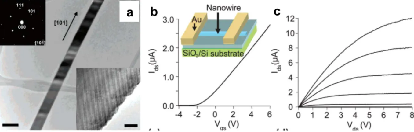
Figure 2.10 a; Low-magnification TEM image of a single Ta-doped SnO2 nanowire with lateral size of ca. 60 nm. Scale bar: 100 nm. Top inset: a selected area electron diffraction (SAED) pattern of the SnO2 nanowire. Bottom inset: a HRTEM image of the same SnO2 nanowire. Scale bar: 5 nm. Transistor characteristics of back-gated Ta-doped SnO2 nanowire FET devices on silicon substrates. b; Current (Ids) vs gate voltage (Vgs) curve at linear region (Vds =1V) for a back-gated NW-FET. Inset: schematic of the device. c; Family of Ids-Vds curves for the same device with Vgs
= 6 to -4 V in -2 V steps from top to bottom[154].
Similarly to ZnO nanowires, SnO2 and In2O3 nanowires were doped with Sb, Ta and other elements, which could favorably substitute the cation in the crystalline nanowire[154]–[156]. In addition, the preparation of nanowires of the ternary system of In-stabilized tin oxide has been investigated[149]. Wan et al. highlights the effect of donor dopants on the electrical properties of tin oxide nanowires, as shown in Figure 2.10. An increased mobility in excess of 100 cm2/Vs was statistically determined from field-effect transistor (FET) devices, and a metallic behavior associated to as low an electrical resistivity as 4 x 10⁻⁴ cm have been recorded though electrical transport measurements[154].
Above demonstrations show that impurity doping is a powerful way to modulate the electrical property of host materials. But since the dynamics of nanowire growth in VLS process is complex (such as two competing crystal growth interfaces), the understanding of doping dynamics is not enough to precisely control the electrical property of metal oxide nanowires. For example,
a b c
34
uncontrollable electrical conductance and inhomogeneity of dopant distribution are found in VLS grown semiconducting oxide nanowires, which are central issues to limit the device applications.
In this study, we also propose a strategy to precisely control the electrical conductivity of doped metal oxide nanowires, which had never been achieved previously.
2.5 Devices applications using metal oxide nanowires
The advance of microelectronics technology has been driven by the thrust of fabricating increasingly smaller devices to create integrated circuits with improved performance and architecture. However, while continuously miniaturizing devices dimension, the existing technologies are approaching their physical limits and inevitably looking for alternative breakthroughs. Bottom-up assembly has demonstrated the capability to produce submicron, nanoscale features, thus offering new opportunities to complement the CMOS technology. As the potential building blocks for future electronics, nanowires exhibit unique physical properties due to their size and structure anisotropy. These properties have been exploited to design and develop various electronic, optoelectronic and mechanical devices. In this context, nanowires represent an ideal channel for electrical carrier transport and are suitable for device integration. In this section, applications based on their electrical and optical properties will be reviewed. Specifically, nanoscale electronic devices such as field-effect transistor, light emitter and detector and chemical sensor will be presented.
2.5.1 Field effect transistor (FET)
One-dimensional nanowires have been fabricated into field-effect transistors to serve as the fundamental building blocks of electronic devices such as logic gate, computing circuits and chemical sensors. Various metal oxides including ZnO, Fe2O3, In2O3, SnO2, Ga2O3, V2O5 and CdO have been configured to FET[107]–[109], [133], [157]–[159]. In brief, the fabrication process can

![Figure 2.2 General schematic for the synthesis of nanowires by deposition of materials into the AAO nanoporous templates[77]](https://thumb-ap.123doks.com/thumbv2/123deta/9847748.1897125/31.918.178.742.105.431/general-schematic-synthesis-nanowires-deposition-materials-nanoporous-templates.webp)

![Figure 2.5 a; Binary phase diagram of Au-Si system, b; Schematic illustration of vapor-liquid- vapor-liquid-solid growth of a Si nanowire or whisker[120]](https://thumb-ap.123doks.com/thumbv2/123deta/9847748.1897125/37.918.290.646.275.677/figure-binary-diagram-schematic-illustration-liquid-nanowire-whisker.webp)
![Figure 2.8 a; Schematics of VLS nanowire growth and vapor-solid (VS) film growth, b; snap shots of crystal growth of molecular dynamics (MD) simulations for VLS formation process, the liquid-solid (LS) interface and VS interface are assigned[138]](https://thumb-ap.123doks.com/thumbv2/123deta/9847748.1897125/42.918.127.795.502.785/schematics-nanowire-molecular-dynamics-simulations-formation-interface-interface.webp)
![Figure 2.9 Schematic of the material flux window concept to design a metal oxide nanowire via the VLS route[47]](https://thumb-ap.123doks.com/thumbv2/123deta/9847748.1897125/43.918.236.686.317.658/figure-schematic-material-window-concept-design-metal-nanowire.webp)