JAIST Repository: Formation of micrometer-order-thick poly-Si films on textured glass substrates by flash lamp annealing of a-Si films prepared by catalytic chemical vapor deposition
20
0
0
全文
(2) Formation of micrometer-order-thick poly-Si films on textured glass substrates by flash lamp annealing of a-Si films prepared by catalytic chemical vapor deposition. K. Ohdaira, T. Fujiwara, Y. Endo, K. Nishioka*, and H. Matsumura Japan Advanced Institute of Science and Technology (JAIST) 1-1 Asahidai, Nomi, Ishikawa 923-1292, Japan Tel: +81-761-51-1563, Fax: +81-761-51-1149, E-mail: [email protected]. We investigate the microstructures of polycrystalline silicon (poly-Si) films formed by flash lamp annealing (FLA) of 4.5-µm-thick precursor a-Si films prepared by catalytic chemical vapor deposition (Cat-CVD) on Cr-coated textured glass substrates. Crystallization of a-Si is performed, keeping the dome-shaped structure formed during deposition of a-Si.. The poly-Si film consists of densely-packed fine grains with sizes. on the order of 10 nm.. The grain size tends to increase approaching the Si/Cr interface,. which can be understood as the result of solid-phase nucleation and following crystallization.. Minority carrier lifetimes of the poly-Si films are worse than those. formed on flat substrates.. This degradation might be due to gaps in the Si layer. 1.
(3) formed during a-Si deposition or FLA. *Present address: Miyazaki University, 1-1, Gakuen Kibanadai Nishi, Miyazaki 889-2192, Japan. PACS codes: 81.10.Jt, 81.40.Ef, 84.60.Jt Keywords: A1. Recrystallization, B2. Semiconducting silicon, B3. Solar cells, A3. Chemical vapor deposition processes,. 2.
(4) 1. Introduction For realization of high-efficiency, highly stable thin-film silicon (Si) solar cells, utilization of polycrystalline Si (poly-Si) formed by post-annealing of precursor amorphous Si (a-Si) has been extensively investigated [1-4].. One of the most. advanced products is a solar cell consisting of poly-Si formed by furnace annealing of a-Si prepared on a glass substrate, which demonstrates conversion efficiency of over 10% [1].. There have been other approaches utilizing large-grained poly-Si layers. formed through aluminum-induced crystallization (AIC) as seed layers for epitaxial growth of thick poly-Si films [3,4].. These crystallization processes require hour-order. processing time or high temperature over 1000 °C. Rapid crystallization of precursor a-Si, instead of conventional furnace annealing, will realize more cost-effective and productive fabrication of thin-film poly-Si solar cells.. For selective heating of. micrometer-thick a-Si without thermal damage to glass, annealing time should be on the order of millisecond, judging from thermal diffusion length of glass and a-Si. By using flash lamp annealing (FLA), with millisecond pulse duration, we have succeeded in forming 4.5-µm-thick high-quality poly-Si on glass substrates, and also have demonstrated solar cell operation using the poly-Si films [5, 6].. Although the. crystallization mechanism has already been partially clarified [7], more in-depth. 3.
(5) understanding will lead to improvement of solar cell efficiency and more productive fabrication processes. In particular, crystallization of a-Si on textured glass might be effective in light trapping, and result in efficiency improvement. In this study, we have compared the microstructures of poly-Si films formed on textured glass substrates to those formed on flat substrates for an understanding of the crystallization mechanism on textured surface by FLA.. Quality of the poly-Si films. has also been investigated, aiming at solar cell application.. 2. Experimental details For fundamental understanding of the crystallization mechanism, we used quartz glass substrates, instead of glass which has poor thermal resistivity, of a 20×20×0.7 mm3 size.. Prior to preparation of precursor a-Si, the quartz surfaces were treated by. reactive ion etching (RIE) using CF4 gas for texture formation. was controlled by changing RIE processing time.. The surface roughness. Cr films 200 nm in thickness were. formed on the textured glass by sputtering at room temperature for the improvement of adhesiveness [5].. Precursor a-Si films with a thickness of 4.5 µm were prepared on the. Cr-coated glass substrates by catalytic chemical vapor deposition (Cat-CVD). Detailed deposition conditions have beem summarized elsewhere [8].. 4. No.
(6) dehydrogenation process was performed prior to FLA.. This is one of the advantages. of Cat-CVD, providing a-Si films with relatively low hydrogen content of about 3%. FLA was performed under fixed duration of 5 ms, and at various irradiances (several tens of J/cm2).. Only one pulse was provided for each sample.. The. microstructures of the poly-Si films formed were characterized by atomic force microscopy (AFM), scanning electron microscopy (SEM), and transmission electron microscopy (TEM).. High-pressure water vapor annealing (HPWVA) was performed. aiming at defect termination of the poly-Si films before estimation of minority carrier lifetime under the optimized condition of 0.9 MPa, 400 °C, and 10 min [9].. The. minority carrier lifetime was measured by microwave photoconductivity decay (µ-PCD) using a pulse laser with a wavelength of 349 nm, and with a photon density of 2×10¹³ /cm2 for carrier excitation.. The poly-Si surface was passivated by iodine/ethanol. solution during µ-PCD measurement.. Considering actual solar cell application,. 10-nm-thick n+-Si layers were inserted between i-Si and Cr films in the poly-Si films for µ-PCD measurement.. We have confirmed there is no significant effect on. crystallization triggered by n+-Si layer insertion.. 3. Results and discussion. 5.
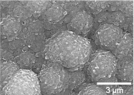
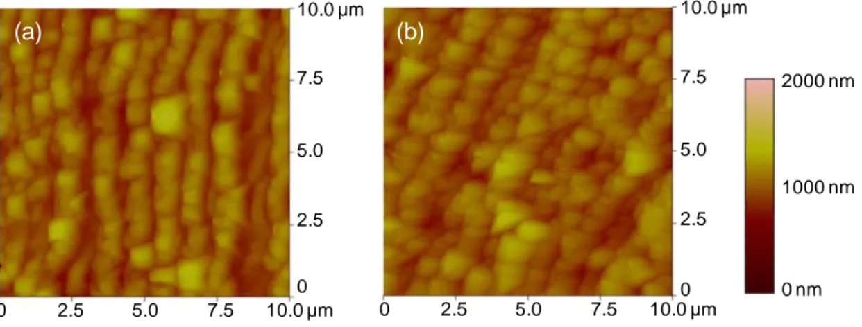
(7) Figure 1(a) shows the AFM image of a quartz surface after 30-min RIE, showing successful texturing of the surface corresponding to root mean square (RMS) roughness of 125 nm.. Precursor a-Si deposited on the Cr-coated textured quartz, and poly-Si. films formed by FLA of the precursor film are shown in Figs 1 (b) and (c), respectively. Crystallization of the Si films has been confirmed by Raman spectroscopy [10]. Dome-shaped structures are clearly observed in the a-Si image.. These are. characteristic structures due to surface roughness of the substrate, and similar structures have already been reported elsewhere [11]. Microstructure of the poly-Si is therefore mainly affected by this initial a-Si structure. Additional structures are seen on the dome surface in the AFM image, which are probably formed by FLA crystallization. The finer structures are clearly observed in the SEM image shown in Fig. 2. This structure might reveal partial peeling of Si due to stress relaxation. These microstructures are greatly different from the poly-Si formed by FLA on a flat glass substrate.. The AFM image of the poly-Si formed on a Cr-coated flat quartz. substrate is shown in Fig. 3(a).. As has been already reported, periodic roughness with. a pitch of about 1 µm is spontaneously formed by crystallization in spite of an originally flat a-Si surface [7]. Similar structure is seen in the AFM image of the poly-Si formed on a Cr-coated quartz substrate with a textured surface having RMS roughness of 46 nm. 6.
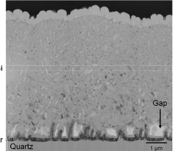
(8) formed by 10-min RIE, shown in Fig. 3(b). This fact indicates that a-Si films on a surface with relatively little roughness can crystallize through a similar mechanism as those on flat substrates. Figure 4 shows the cross-sectional TEM image of the poly-Si on a Cr-coated quartz substrate textured for 30 min by RIE. order of 10 nm.. The poly-Si consists of grains with sizes of the. Interestingly, the grain size tends to increase approaching the Si/Cr. interface. This phenomenon can be understood by considering solid-phase nucleation and following solid-phase growth.. Temperature of Si during FLA must be higher in. the upper part than at the bottom because more flash lamp light is absorbed in the surface region, although the difference is likely to be significantly relaxed due to thermal diffusion.. According to classical nucleation theory, solid phase nucleation. occurs more rapidly under higher temperature, with strong temperature dependence of. {(. ) }. exp − E f + E m + ΔG ∗ kT , where Ef, Em, and ΔG* represent the activation energy. for defect generation, that for defect jump, and the maximum value of the cluster free energy curve, respectively [12].. Furthermore, considering an undercooling. temperature of 269 K (from the difference between crystalline and a-Si melting points of 1414 and 1145 °C, respectively), nucleation rate from molten Si is negligible during millisecond treatment [13].. This grain size distribution can therefore be explained. 7.
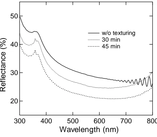
(9) only by the difference of solid-phase nucleation rate due to temperature distribution during FLA. The cross-sectional TEM image shown in Fig. 4 is significantly different from that of poly-Si formed on a flat substrate, showing the alternative features of relatively large (>100 nm) grain regions and fine (~10 nm) grain regions connecting to the periodic surface roughness [14]. This difference probably comes from different crystallization mechanisms.. We have understood the characteristic crystallization of a-Si on a flat. glass substrate as the repeated effect of thermal generation due to crystallization and transfer of the generated heat to neighboring a-Si, resulting in lateral growth from edge to center of the sample, and consequent surface roughness perpendicular to the lateral growth direction [14].. This thermal transfer from crystallized to uncrystallized parts. seems to be less effective in the case of a-Si deposited on a textured substrate, because of the initial dome-shaped structure. a-Si on a textured substrate therefore receives thermal energy mainly from direct flash lamp light, and the cross-sectional image of the poly-Si shows no evidence of lateral crystallization. Finally, we discuss the potential of the poly-Si films as solar cell material.. Figure. 5 shows reflectance spectra of the poly-Si films formed on the textured substrates. Reduction of the reflectance occurs with increase in the texturing time, indicating more. 8.
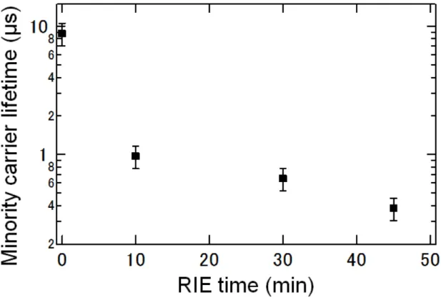
(10) effective light trapping on the poly-Si film surfaces formed on the textured substrates. On the other hand, the minority carrier lifetimes of the poly-Si films shows significant reduction with increasing RIE time as shown in Fig. 6.. Note that the poly-Si on the. 10-min RIE textured glass substrate, showing similar surface morphology to that on a flat substrate, also reflects a worse lifetime. This degradation might be due to gaps in the Si films formed during a-Si deposition or crystallization by FLA, particularly observed close to Cr in the TEM image (Fig. 4).. Based on these results, further. structural improvement, such as utilization of less sharpened textured substrates, will be necessary for solar cell application of the poly-Si films formed on textured substrates.. 4. Conclusion We have clarified crystallization mechanism of a-Si deposited on textured glass substrates by FLA from the microstructure of the formed poly-Si.. Crystallization. occurs, keeping the dome-shaped structure formed during a-Si deposition. The grain size tends to increase approaching the Si/Cr interface, which is a clear indication of solid-phase nucleation.. Minority carrier lifetimes of the poly-Si films formed on. textured substrates tend to degrade, which might be due to gaps in the Si film generated during a-Si deposition or FLA.. 9.
(11) Acknowledgments The authors acknowledge T. Owada and T. Yokomori of Ushio Inc. for their expert operation of and fruitful discussion on FLA.. This work was supported by the New. Energy and Industrial Technology Development Organization (NEDO) of Japan.. References [1] M. J. Keevers, T. L. Young, U. Schubert, and M. A. Green, Proc. 22nd European Photovoltaic Sol. Energy Conf. (2007) 1783. [2] A. G. Aberle, P. I. Widenborg, P. Campbell, A. Sproul, M. Griffin, J.W. Weber, B. Beilby, D. Inns, M. Terry, T. Walsh, O. Kunz, S. He, C.Y. Tsao, Z. Ouyang, J. Wong, B. Hoex, L. Shi, T. Sakano, M. Wolf, J. Huang, G. Jin, L. Huang, S. Peng, M. Lang, D. Schmunk, F. Bamberg, S.V. Chan, J. Han, T. Ruof, O. Berger, D. Di, A. Fattal, P. Gress, M. Pelletier, E. Mitchell, Y. Zhou, F. Fecker, and S. Pohlner, Proc. 22nd European Photovoltaic Sol. Energy Conf. (2007) 1884. [3] L. Carnel, I. Gordon, D. Van Gestel, G. Beaucarne, and J. Poortmans, Proc. 22nd European Photovoltaic Sol. Energy Conf. (2007) 1880. [4] I. Gordon, L. Carnel, D. Van Gestel, G. Beaucarne, J. Poortmans, L. Pinckney, and A.. 10.
(12) Mayolet, Proc. 22nd European Photovoltaic Sol. Energy Conf. (2007) 1993. [5] K. Ohdaira, Y. Endo, T. Fujiwara, S. Nishizaki, and H. Matsumura, Jpn. J. Appl. Phys. 46 (2007) 7603. [6] K. Ohdaira, T. Fujiwara, Y. Endo, K. Shiba, H. Takemoto, S. Nishizaki, Y. R. Jang, K. Nishioka, and H. Matsumura, Proc. 33rd IEEE Photovoltaic Specialists Conf. (2008) (in press) [7] K. Ohdaira, T. Fujiwara, Y. Endo, S. Nishizaki, K. Nishioka and H. Matsumura, Proc. 17th Int. Photovoltaic Science and Engineering Conf., (2007) 1326. [8] K. Ohdaira, S. Nishizaki, Y. Endo, T. Fujiwara, N. Usami, K. Nakajima, and H. Matsumura, Jpn. J. Appl. Phys. 46 (2007) 7198. [9] Y. Endo, T. Fujiwara, S. Nishizaki, K. Ohdaira, K. Nishioka and H. Matsumura, Proc. 17th Int. Photovoltaic Science and Engineering Conf., (2007) 319. [10] T. Fujiwara, Y. Endo, S. Nishizaki, K. Ohdaira, K. Nishioka and H. Matsumura, Proc. 17th Int. Photovoltaic Science and Engineering Conf., (2007) 1157. [11] H. Iida, T. Mishiku, A. Ito, and Y. Hayashi, IEEE Trans. Electron Devices, ED-34 (1987) 271. [12] C. Spinella and S. Lombardo, J. Appl. Phys. 84 (1998) 5383. [13] R. P. Liu, T. Volkmann, and D. M. Herlach, Acta Mater. 49 (2001) 439.. 11.
(13) [14] K. Ohdaira, T. Fujiwara, Y. Endo, S. Nishizaki, K. Nishioka, and H. Matsumura, submitted to Sol. Energy Mat. Sol. Cells. 12.
(14) Figure captions Fig. 1. Surface AFM images of (a) quartz textured by 30-min RIE, (b) a-Si deposited. on glass, and (c) poly-Si formed by FLA of the a-Si. Fig. 2. SEM image of the poly-Si surface formed on the quartz substrate textured for. 30 min. Fig. 3 AFM images of poly-Si films formed on (a) flat and (b) 10-min RIE-textured quartz substrates. Fig. 4 Cross-sectional TEM image of the poly-Si formed on the quartz substrate textured for 30 min. Fig. 5. Reflectance spectra of the poly-Si films as a function of RIE time.. Fig. 6. Minority carrier lifetimes of the poly-Si films as a function of RIE time.. 13.
(15) 10.0 µm. 10.0 µm. (a). 0. (b). 2.5. 5.0. 7.5. 7.5. 7.5. 5.0. 5.0. 2.5. 2.5. 0 10.0 µm. 0. 2.5. 10.0 µm. (c). 2000 nm 7.5. 1000 nm. 5.0. 2.5 0 nm 0. 2.5. 5.0. 7.5. 0 10.0 µm. Fig. 1. K. Ohdaira et al.,. 14. 5.0. 7.5. 0 10.0 µm.
(16) Fig. 2. K. Ohdaira et al.,. 15.
(17) 10.0 µm. 10.0 µm. (a). (b) 7.5. 7.5. 5.0. 5.0. 2000 nm. 1000 nm 2.5. 2.5. 0. 2.5. 5.0. 7.5. 0 10.0 µm. Fig. 3. 0. 2.5. 5.0. K. Ohdaira et al.,. 16. 7.5. 0 10.0 µm. 0 nm.
(18) Fig. 4. K. Ohdaira et al.,. 17.
(19) Reflectance (%). 50 w/o texturing 30 min 45 min. 40. 30. 20 300. 400. 500. 600. Wavelength (nm) Fig. 5. K. Ohdaira et al.,. 18. 700. 800.
(20) Fig. 6. K. Ohdaira et al.,. 19.
(21)
図

+3
関連したドキュメント
6 HUMAN DETECTION BY TILTED SENSORS FROM CEILING Based on previous studies, this paper presents an approach to detect human 2D position, body orientation and motion by using
performed 4 h and 8 h euglycemic (5.5 mmol/l) clamps with 3 different insulin concentrations (basal, medium postprandial and high postprandial, ranging from ~ 35 to ~ 1450 pmol/l)
Keiji YAMADA, Takashi UEDA, Yasuharu UENO, Yoshinori FUNADA, Kaoru AWAZU and Tadaaki SUGITA In order to evaluate the mechanical properties of diamond-like carbonDLC thin films formed
reduction.. Change in Vickers hardness as a function of annealing temperature for cold-rolled pure iron, Fe-0.3mass%Si alloy and Fe-0.3mass%Al alloy with 99.8%. reduction
Upon exposure to a catalytic amount of Rh I , homopropargylallene-alkynes 5 effected a novel cycloisomerization accompanied by the migration of alkyne moiety of
The study on the film of the block copolymer ionomer with a cesium neutralized form (sCs-PS- b -f-PI) revealed that a small amount of water and thermal annealing promoted the
Provided that the reduction of the time interval leads to incomparableness of normalized bubble-size distributions and does not change the comparable distributions in terms of
The C-minor partial orders determined by the clones gen- erated by a semilattice operation (and possibly the constant operations corresponding to its identity or zero elements)
