Atomic diffusion bonding of Si wafers using
thin Nb films
著者
Miyuki Uomoto, Takehito Shimatsu
journal or
publication title
Japanese Journal of Applied Physics
volume
59
number
SB
page range
SBBC04-1-SBBC04-3
year
2019-11-27
URL
http://hdl.handle.net/10097/00129723
doi: 10.7567/1347-4065/ab4b1cJapanese Journal of Applied Physics 59, SBBC04(1-3) (2020) DOI:10.7567/1347-4065/ab4b1c
1
Atomic Diffusion Bonding of Si Wafers using Thin Nb Films
Miyuki Uomoto1, and Takehito Shimatsu1,2,3*
1 Frontier Research Institute for Interdisciplinary Sciences (FRIS), Tohoku University, Sendai 980-8578, Japan 2 Research Institute of Electrical Communication (RIEC), Tohoku University, Sendai 980-8577, Japan 3 Center for Spintronics Research Network (CSRN), Tohoku University, Sendai 980-8577, Japan
*E-mail: [email protected]; [email protected]
This study of atomic diffusion bonding of Si wafers in vacuum using thin Nb films reveals remarkably high bonding strength, greater than fracture strength of a Si wafer, obtained using Nb films at thicknesses of 1.7–20 nm on each side. Transmission electron microscopic cross-section images show no vacancy at the bonded interface. Particularly, crystal lattice rearrangement occurs to a remarkable degree at the bonded interface of 10-nm-thick Nb films. Surface roughness reduction is likely to enhance the crystal lattice rearrangement at the bonded interface, even with thick Nb films.
Bonding of two flat wafers in vacuum using thin metal films (atomic diffusion bonding, ADB)1,2) is a promising
candidate process to achieve wafer bonding at room temperature along with surface-activated bonding3–6).
When using ADB, any mirror-polished wafer can be bonded using almost any metal film including materials having high melting points such as tungsten. Niobium, which shows a high superconducting transition temperature in single metals, is used for superconducting accelerators.7,8) For superconducting devices, reliable
bonding between Nb to Nb is necessary.
We examined the interface structure of Nb films bonded using ADB. An ultra-high vacuum (UHV) DC-magnetron sputtering system was used for film deposition. The vacuum chamber’s base pressure was less than 1 × 10⁻⁶ Pa.
Si wafers were used for this study. Surface roughness Sa
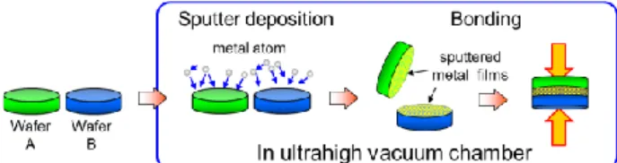
evaluated using atomic force microscopy (AFM) for Si wafers was 0.13 nm. Immediately after fabricating Nb films on the surfaces of two Si wafers using sputter deposition, the two Nb films on the wafers were bonded in the same vacuum, as shown in Figure 1. No substrate heating was conducted during deposition or bonding processes. We observed the Nb film interface structure for Si wafers bonded using 20-nm-thick Nb film on each side.9)
Transmission electron microscopy (TEM) images revealed no vacancy at the bonded interface. However, a low-density amorphous-like structure was partially observed at the bonded interface, which is expected to have a bad influence on superconducting properties at the interface. Nevertheless, it is reasonable to infer that the interface structure depends on the film thickness, as is true also for ADB using other films such as Ti10) and Au11), and which
can be improved by reducing surface roughness. The surface free energy at the bonded interface of the bonded Si wafers can not be evaluated using the blade method with Maszara’s equation12) because the blade can not be inserted
between the wafers, indicating that the interface bonding strength is greater than the fracture strength of Si wafers. However, the value of is expected to depend on the Nb film thickness as well, as is true also for ADB using the other films such as Ti and W10). As described herein, after
examining the thickness dependence of for wafers bonded using Nb films, we assess the interface structure of wafers bonded using thin Nb films.
Figure 2 presents the values of for Si wafers bonded
using Nb films as a function of the Nb film thickness on each side, . As increased, increased and became greater than the surface energy of Nb13–15), E
s(Nb), at of 1 nm. A
further increase of enhanced . The values for of 1.7– 20 nm were not evaluated because the blade could not be inserted between the wafers, indicating remarkably high bonding strength. The blade was inserted between the Si wafers for of 30 nm, indicating reduction of . Nevertheless, we were unable to estimate values using the blade method for of 30 nm because optical light for the infrared image camera was insufficient to penetrate the thickly bonded Nb films. The reduction of with increasing over a critical film thickness is commonly observed in ADB10). The increase of film thickness enhanced the
surface roughness, leading to poor interface diffusion between the two connected films in that thick region.
Fig. 1. Schematic illustration of the bonding process.
Fig. 2. Surface free energy values at the bonded interface for Si wafers bonded using Nb films as a function of Nb film thickness on each side, .
Japanese Journal of Applied Physics 59, SBBC04(1-3) (2020) DOI:10.7567/1347-4065/ab4b1c
2
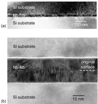
Figure 3 shows TEM cross-section images of Si wafers bonded using Nb (10 nm) film on each side, with (a) low and (b) high magnifications. Those for Si wafers bonded using Nb (20 nm) film on each side were also shown for compariosn in Figure 4. By reducing the Nb film thickness from 20 nm to 10 nm, the amorphous-like structure at the bonded interface disappeared. Crystal lattice rearrangement occurred remarkably at the bonded interface for wafers bonded using Nb (10 nm) film on each side.
Fig. 3. TEM cross-section images of bonded Si wafers using Nb (10 nm) film on each side, with (a) low magnification and (b) high magnification.
Fig. 4. TEM cross-section images of bonded Si wafers using Nb (20
nm) film on each side, with (a) magnification and (b) high magnification.
Figure 5 presents X-ray diffraction patterns of single Nb films with respective film thicknesses of 10 nm and 20 nm. These films are deposited under the same condition for the films used for bonding. X-ray diffraction patterns showed that films have (110) preferred grain orientation parallel to the film plane. No significant difference was observed between these films in terms of the preferred grain orientation, which indicates that the variation of preferred grain orientation is not the origin of the difference in their bonded interface structures.
Figure 6 depicts AFM surface images of Nb films with the respective film thicknesses of 10, 20, 30 and 50 nm. Values of Sa evaluated from AFM images are shown as a
function of Nb film thickness in Figure 7. The Sa value of
Si wafer surface is shown as a dotted line in the figure. Sa
decreased monotonically as the thickness decreased, approaching Sa of Si wafers when the Nb thickness is zero.
In actuality, Sa for 10-nm-thick Nb film was 0.20 nm,
which was considerably smaller than that for 20-nm-thick Nb film (Sa=0.29 nm). For wafers bonded using Nb (10
nm) film on each side, it is likely that the remarkable crystal lattice rearrangement occurred at the bonded interface mainly because of the reduction of Sa by
reducing the Nb film thickness.
Our experimentally obtained results demonstrated that the interface structure for bonded Nb/Nb films is affected sensitively by the Nb film surface roughness. One can reasonably infer that this results from a small self-diffusion coefficient D for Nb. The value of D for Nb at room temperature (300 K), calculated from the values of the frequency factor D0 and the activation energy Q,16)
is 1.1×10–74 m2/s, which is considerably less than those of
representative material films used for ADB such as Ti (D=6.6×10–36 m2/s) and Al (D=3.2×10⁻²⁹ m2/s).
Thick Nb films with a smooth film surface are necessary for application to superconducting accelerators. Energy treatment sputtering (ETS)17) is one solution for
this difficulty: ETS, which is sputter film deposition performed coincidently with slight etching of the advancing surface during film growth using an ion-beam, is useful to fabricate thick films with an extremely smooth surface. ADB using thick ETS-Nb films is expected to be useful for practical applications.
Fig. 5 X-ray diffraction patterns of single Nb films with respective
Japanese Journal of Applied Physics 59, SBBC04(1-3) (2020) DOI:10.7567/1347-4065/ab4b1c
3
Fig. 6 AFM surface images of Nb films with film thicknesses of 10,
20, 30, and 50 nm.
Fig. 7 Values of Sa evaluated from AFM images as a function of Nb
film thickness.
1) T. Shimatsu and M. Uomoto, J. Vac. Sci. Technol. B 28, 706 (2010).
2) T. Shimatsu and M. Uomoto, ECS Trans. 33(4), 61 (2010). 3) T. Suga, K. Miyazawa, and Y. Yamagata, MRS Int. Meet. Adv.
Mater. 8, 257 (1989).
4) T. Suga, Y. Takahashi, H. Takagi, B. Gibbesch, and G. Elssner, Acta Metall. Mater. 40, s133 (1992).
5) H. Takagi, K. Kikuchi, R. Maeda, T. R. Chung, and T. Suga, Appl. Phys. Lett. 68, 2222 (1996).
6) E. Higurashi, T. Imamura, T. Suga, and R. Sawada, IEEE Photonics Technology Letters, 19, 1994 (2007).
7) A.-M. Valente-Feliciano, Supercond. Sci. Technol. 29, 113002 (2016).
8) H. Padamsee, Supercond. Sci. Technol. 30, 053003 (2017). 9) M. Uomoto, and T. Shimatsu, Proc. 6th Int. Workshop Low
Temperature Bonding for 3D Integration, 65 (2019) [DOI: 10.23919/LTB-3D.2019.8735105.]
10) T. Shimatsu and M. Uomoto, ECS Trans. 64 [5], 317 (2014). 11) S. Matsuda, M. Uomoto, A. Miura, and T. Shimatsu, Proc. 6th Int.
Workshop Low Temperature Bonding for 3D Integration, 67 (2019) [DOI: 10.23919/LTB-3D.2019.8735204.]
12) M. P. Maszara, G. Goetz, A. Cavigila, and J. B. McKitterick, J. Appl. Phys. 64, 4943 (1988).
13) L. Vitos, A.V. Ruban, H.L. Skriver, and J. Kolla´r, Surface Science 411, 186 (1998).
14) W. R. Tyson, W. A. Miller, Surf. Sci. 62, 267 (1977).
15) F. R. de Boer, R. Boom, W. C. M. Mattens, A. R. Miedema, A. K. Niessen, Cohesion in Metals, North-Holland, Amsterdam (1988). 16) The Japan Institute of Metals, Metal Data Book, p20, Maruzen,
Japan (1993).
17) T. Saito, H. Makita, T. Moriwaki, Y. Suzuki, N. Kato, S. Wakayanagi, A. Miura, M. Uomoto, and T. Shimatsu, Proc. 6th Int. Workshop Low Temperature Bonding for 3D Integration, 64 (2019) [DOI: 10.23919/LTB-3D.2019.8735262.]