INVITED PAPER
Special Section on Electronic DisplaysFrequency Characteristics of Polymer Field-E
ffect Transistors with
Self-Aligned Electrodes Investigated by Impedance Spectroscopy
Hideyuki HATTA†, Takashi NAGASE†,††a), Takashi KOBAYASHI†,††, Mitsuru WATANABE†††, Kimihiro MATSUKAWA†††, Shuichi MURAKAMI††††, Nonmembers, and Hiroyoshi NAITO†,††b), Member
SUMMARY Solution-based organic field-effect transistors (OFETs) with low parasitic capacitance have been fabricated using a self-aligned method. The self-aligned processes using a cross-linking polymer gate insulator allow fabricating electrically stable polymer OFETs with small overlap area between the source-drain electrodes and the gate electrode, whose frequency characteristics have been investigated by impedance spec-troscopy (IS). The IS of polymer OFETs with self-aligned electrodes re-veals frequency-dependent channel formation process and the frequency response in FET structure.
key words: organic field-effect transistors, frequency response, self-aligned method, impedance spectroscopy, cross-linking polymer insulators
1. Introduction
Organic field-effect transistors (OFETs) have attracted growing interest as a key technology for realizing low-cost, large-area, and flexible active-matrix displays such as or-ganic light-emitting diode displays and electronic papers. For the application of OFETs to high-speed devices includ-ing gate drivers and logic circuits, the understandinclud-ing of the frequency response of OFETs is of crucial importance. The frequency characteristics of OFETs have been extensively studied by utilizing metal-insulator-semiconductor (MIS) structure by impedance spectroscopy (IS) [1]–[5]. The IS of organic MIS diodes has revealed charge relaxation process associated with channel formation [2] at the organic semi-conductor/gate insulator interface on the basis of the anal-ysis using equivalent circuits. It has been reported that the IS of organic MIS diodes also gives information concerning the doping density of organic semiconductor layers [1], in-terfacial trap states [4], and charge mobility in the semicon-ductor bulk [3]. The impedance measurements using FET structure are also attractive because they enable the direct determination of the response speed of OFETs and the
in-Manuscript received March 2, 2011. Manuscript revised June 8, 2011.
†The authors are with the Department of Physics and
Electron-ics, Osaka Prefecture University, Sakai-shi, 599-8531 Japan.
††The authors are with the Research Institute for Molecular
Electronic Devices, Osaka Prefecture University, Sakai-shi, 599-8531 Japan.
†††The authors are with the Department of Electronic
Materi-als, Osaka Municipal Technical Research Institute, Osaka-shi, 536-8533 Japan.
††††The author is with the Technology Research Institute of Osaka
Prefecture, Izumi-shi, 594-1157 Japan. a) E-mail: [email protected] b) E-mail: [email protected]
DOI: 10.1587/transele.E94.C.1727
vestigation of the parasitic impedance of practical OFETs. Several authors have reported the impedance measurements of OFETs with thermally grown SiO2 gate insulators [6]–
[8]. It is well known that the electrical characteristics of OFETs sensitively depend on the surface properties of gate insulators owing to the self-organization behavior of organic semiconducting molecules [9]. For practical applications, the investigation of the frequency characteristics of solution-based OFETs with polymer gate insulators is required.
To increase the response speed of OFETs, improving device configurations as well as field-effect mobility μ is also important. The cutoff frequency fT of FET devices is
defined as the frequency when ac input and output current become the same amplitude (unity gain) and is given by
fT = μV G 2πL2 1 1+ Cp W LCi , (1)
where VGis the gate voltage, L is the channel length, Cpis
the parasitic capacitance, W is the channel width, and Ciis
the capacitance per unit area of the gate insulator. Based on this model, shrinking L and improving μ increase the
fT. However, conventional OFETs generally have high
par-asitic capacitance caused by large overlap area between the source-drain electrodes and the gate electrode, which limits the response speed of practical OFETs [10]. The decrease in the parasitic capacitance of OFETs is, therefore, required for the fabrication of high-speed OFET circuits. To reduce the parastic capasitance of OFETs, Okada et al. [11], [12] have adopted a self-aligned method, initially proposed for amor-phous Si thin-film transistors [13], [14], for the fabrication of pentacene-based OFETs. More recently, the fabrication of high-speed printed OFETs with top-gate configurations has been demonstrated using the self-aligned method com-bining with inkjet printing [15].
In this paper, we report the self-aligned method for solution-based OFETs with bottom-gate configurations and the frequency characteristics investigated by the IS. The present method enables to fabricate electrically stable poly-mer OFETs having low parasitic capacitance without any lithographic damage to organic semiconductor layers. The decrease in the parasitic capacitance of OFETs with self-aligned electrodes is verified by capacitance measurements using the IS. We also show that the IS of self-aligned OFETs provides information on channel formation process and cut-off frequency in the OFET structure.
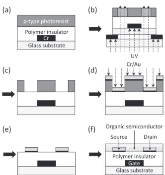
Fig. 1 Schematics of the fabrication processes of solution-based OFETs with polymer gate insulators using the self-aligned method.
2. Experiments
The schematics of the fabrication processes of solution-based OFETs using the self-aligned method are shown in Fig. 1. A micrometer wide Cr gate electrode was de-fined on a glass substrate by photolithography. The width of the Cr electrode was 50μm. We used the cross-linking organic-inorganic hybrid polymer dielectric of poly (methylsilsesquioxane) (PMSQ) [9], [16], which was pre-pared in our laboratory, as a polymer gate insulator. The PMSQ layer was fabricated onto the substrate by spin coat-ing, followed by curing at 150◦C for 1 h in ambient air. The thickness of PMSQ insulator layers was 300–400 nm. The cured PMSQ films are not dissolved in commonly used or-ganic solvents, which enables us to perform the following lithographic processes on the polymer gate insulators. Af-ter preparing the PMSQ layer, a positive-type photoresist (Microposit S1818, Rohm&Haas) was spin-coated onto the PMSQ surface [Fig. 1(a)]. Then, the resist layer was ex-posed to UV light from back surface through a glass pho-tomask using a mask aligner [Fig. 1(b)], and the exposed area of the resist layer was removed using an alkaline devel-oper (TMAH 2.38%) [Fig. 1(c)]. In this process, the Cr gate electrode acts as a shadow mask and resist patterns can be formed on the channel region of OFETs. Next, Cr (1–2 nm) and Au (40 nm) were successively evaporated on patterned structure [Fig. 1(d)], and the electrode metals deposited on the resist were removed by a lift-off technique [Fig. 1(e)]. Using these processes, the electrode configuration with a small overlap area between source-drain and gate electrodes can be fabricated. Finally, a p-type organic semiconduc-tor of poly (2,5-bis (3-hexadecylthiophene-2-yl) thieno
[3,2-Fig. 2 Experimental setup for the impedance measurements of OFETs used in this study.
b] thiophene) (PBTTT) [17]–[19] was cast onto the PMSQ layer from a 0.1 wt% toluene solution [Fig. 1(f)]. The L and
W of self-aligned PBTTT FETs were 50μm and 2.4 mm,
respectively. Note that in this approach the organic semi-conductor layer does not suffer from any lithographic dam-age such as UV exposure and immersion in organic solvents during the fabrication of self-aligned OFETs. For compar-ison, PBTTT FETs with a none-defined indium-tin-oxide gate electrode were also fabricated on PMSQ gate insula-tors. Their L and W were 50μm and 3.0 mm, respectively.
The electrical measurements of fabricated OFET de-vices were performed in a vacuum probe station (Desert Cryogenics TTP-4) at room temperature. For FET measure-ments, Keithley 2611 and 2400 source meters were used. Impedance measurements were performed using a Solartron 1260 impedance analyzer with a 1296 dielectric interface. The complex impedance Z was measured by applying a dc
VGwith an ac voltage of±100 mV to the source and drain
electrodes according to the configuration shown in Fig. 2.
3. Results and Discussion
Figure 3 shows the optical microscope image of PBTTT FET with L=50 μm fabricated using the self-aligned method. It can be seen that the boundaries between the source-drain electrodes and the gate electrode are clearly formed. To evaluate the parasitic capacitance between source-drain and gate electrodes, we measured the ca-pacitance of both electrode configurations fabricated us-ing the self-aligned and conventional methods by the IS (Fig. 4). The conventional electrode configuration has high capacitance, whereas the self-aligned electrode configura-tion has considerably-low capacitance of ∼1 pF, due to a small overlapping of electrodes. We also see that the capac-itance remains unchanged for frequency sweep from 1 Hz to 100 kHz. This is attributed to an extremely low density of ionic impurities of our PMSQ gate insulators [9], [16].
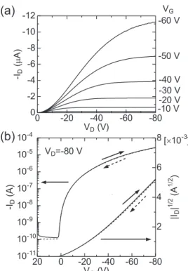
Figure 5 shows the output (drain current ID-drain
volt-age VD) and transfer (ID-VG) characteristics of PBTTT FET
with self-aligned electrodes. The output characteristics show clear IDsaturation, whereas the ID is nonlinearly
in-creased in the low VDregion. Such nonlinear ID-VD
charac-teristics are also observed in PBTTT FETs fabricated us-ing the conventional method (not shown) and can be at-tributed to the formation of Schottky barriers for hole in-jection caused by the potential difference between the work
Fig. 3 Optical microscope image of PBTTT FET with L=50 μm fabricated using the self-aligned method.
Fig. 4 Frequency dependence of capacitance between the source-drain electrodes and the gate electrode of electrode configurations fabricated us-ing the self-aligned and conventional methods.
function of source Au electrode (4.9 eV) and the ionization potential of PBTTT semiconductor (5.1 eV) [20]. The sat-uration field-effect mobility and on/off ratio estimated from the transfer characteristics, respectively, are 0.013 cm2/Vs
and 2.4 × 10⁵, which are comparable to those of the devices
fabricated using the conventional method. It can be seen that the transfer characteristics show no hysteresis with respect to the VGsweep. This is attributed to the low density of
hy-droxyl (OH) groups of PMSQ gate insulators [9], [16]. It has been reported that OH groups act as electron trapping sites [21], [22] and the decrease in OH groups at the semicon-ductor/insulator interface suppresses the hysteresis behavior of OFETs [23]. The self-aligned processes also allow the reliable fabrication of OFETs having lower off current and better subthreshold characteristics because small electrode overlapping reduces the leakage current of gate insulators [14]. Highly stable, solution-based OFETs having low par-asitic capacitance are successfully fabricated using the self-aligned method and cross-linking PMSQ gate insulators.
Figure 6 shows the C-VG characteristics of PBTTT
FETs with conventional and self-aligned electrode config-urations. The capacitance between the source-drain elec-trodes and the gate electrode of the devices with self-aligned electrode configurations is increased when the negative VG
is applied. This clearly indicates that the holes are injected from the source and drain electrodes and accumulated in the channel region. In contrast, the devices with conventional
Fig. 5 (a) Output and (b) transfer characteristics of PBTTT FET with L=50 μm fabricated using the self-aligned method.
Fig. 6 Capacitance-gate voltage characteristics of PBTTT FETs fabricated using the self-aligned and conventional methods.
electrode configurations show high capacitance, which pre-vents the measurement of a small change of capacitance as-sociated with hole accumulation.
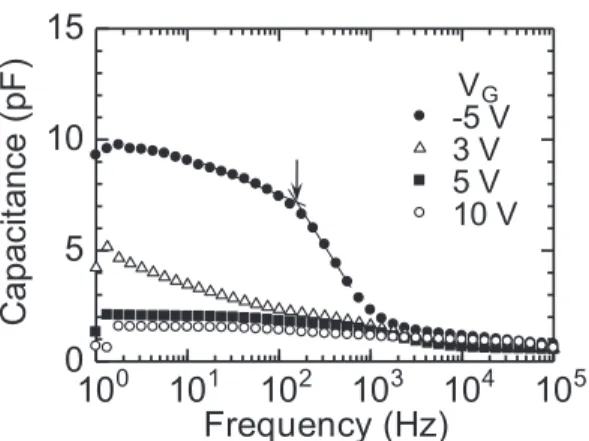
Figure 7 shows the frequency dependence of capaci-tance (C- f ) of self-aligned PBTTT FET measured at differ-ent VG. When the positive VG is applied, the capacitance
displays a small value that is almost independent of the fre-quency, indicating the formation of the depletion layer in the channel region. The capacitance is remarkably increased when the polarity of VGis altered from the positive to the
negative. The gradual increase in the capacitance in the low frequency regime has frequently been observed in organic MIS diodes [3], [5] and would stem from hole accumulation at the peripheral area around the channel.
de-Fig. 7 Capacitance-frequency characteristics measured at different VGin
PBTTT FET with L=50 μm fabricated using the self-aligned method.
creased with increasing frequency and approaches∼1 pF at higher frequencies, resulting from the frequency-dependent channel formation in OFETs. In the low frequency regime, the injected holes follow the frequency and are accumulated uniformly in the channel region. Meanwhile, the injected holes cannot follow higher frequency owing to the limit of charge transport, which prevents the uniform hole accumu-lation in the channel region and results in the decrease in the capacitance. Therefore, the high-frequency limit of OFETs can be directly determined from C- f characteristics. The cutoff frequency determined from the inflection point of the
C- f characteristic measured at VG=−5 V is approximately
150 Hz. This value is lower than the theoretical cutoff fre-quency of 410 Hz, which was calculated from Eq. (1) using
Cp=0 F. The discrepancy between theory and experiment
is likely to be caused by the parasitic contact resistance of PBTTT FETs with Au source-drain electrodes. It has been reported that a high contact resistance of PBTTT FETs with Au electrodes reduces effective field-effect mobility in the low voltage region [18], which results in the decrease in the cutoff frequency. These results suggest that increasing field-effect mobility as well as reducing parasitic impedance is essential to improve the frequency response of practical OFETs.
4. Conclusions
We have fabricated solution-based OFETs with polymer gate insulators by the self-aligned method. It was demon-strated that the self-aligned processes using cross-linking PMSQ gate insulators enable the fabrication of electrically stable polymer OFETs with low parasitic capacitance. We have investigated the frequency characteristics of OFETs us-ing the IS. The VG and frequency dependence of channel
formation process in OFETs is clearly observed by using the OFETs with self-aligned electrodes. The presented re-sults are useful for the fabrication of high-speed OFETs and for a deep understanding of frequency response of OFETs.
Acknowledgments
This work was supported by a Grant-in-Aid for Scientific Research (B) (No. 23360140) from the Japan Society for the Promotion of Science (JSPS), by a Grant-in-Aid for Young Scientists (B) (No. 21710140) from the Ministry of Educa-tion, Culture, Sports, Science and Technology (MEXT) of Japan, and by a Funding Program for World-Leading Inno-vative R&D on Science and Technology (FIRST Program) form JSPS.
References
[1] E.J. Maijer, A.V.G. Mangnus, C.M. Hart, D.M. de Leeuw, and T.M. Klapwijk, “Frequency behavior and the Mott-Schottky analysis in poly (3-hexyl thiophene) metal-insulator-semiconductor diodes,” Appl. Phys. Lett., vol.78, pp.3902–3904, 2001.
[2] I. Torres, D.M. Taylor, and E. Itoh, “Interface states and depletion-induced threshold voltage instability in organic metal-insulator-semiconductor structures,” Appl. Phys. Lett., vol.85, pp.314–316, 2004.
[3] S. Grecu, M. Bronner, A. Opitz, and W. Br¨utting, “Characterization of polymeric metal-insulator-semiconductor diodes,” Synth. Met., vol.146, pp.359–363, 2004.
[4] I. Torres and D.M. Taylor, “Interface states in polymer metal-insulator-semiconductor devices,” J. Appl. Phys., vol.98, 073710, 2005.
[5] E. Itoh and K. Miyairi, “Interfacial charge phenomena at the semi-conductor/gate insulator interface in organic field effect transistors,” Thin Solid Films, vol.499, pp.95–103, 2006.
[6] T. Miyadera, M. Nakayama, S. Ikeda, and K. Saiki, “Investigation of complex channel capacitance in C60field effect transistor and
eval-uation of the effect of grain boundaries,” Curr. Appl. Phys., vol.7, pp.87–91, 2007.
[7] T. Miyadera, T. Minari, K. Tsukagoshi, H. Ito, and Y. Aoyagi, “Frequency response analysis of pentacene thin-film transistors with low impedance contact by interface molecular doping,” Appl. Phys. Lett., vol.91, 013512, 2007.
[8] B.H. Hamadani, C.A. Richter, J.S. Suehle, and D.J. Gundlack, “In-sights into the characterization of polymer-based organic thin-film transistors using capacitance-voltage analysis,” Appl. Phys. Lett., vol.92, 203303, 2008.
[9] T. Nagase, T. Hamada, K. Tomatsu, S. Yamazaki, T. Kobayashi, S. Murakami, K. Matsukawa, and H. Naito, “Low-temperature pro-cessable organic-inorganic hybrid gate dielectrics for solution-based organic field-effect transistors,” Adv. Mater., vol.22, pp.4706–4710, 2010.
[10] M. Kitamura and A. Arakawa, “Current-gain cutoff frequencies above 10 MHz for organic thin-film transistors with high mobility and low parasitic capacitance,” Appl. Phys. Lett., vol.95, 023503, 2009.
[11] T. Hyodo, F. Morita, H. Okada, and H. Onnagawa, “Self-aligned organic field-effect transistors using back-surface exposure method,” Jpn. J. Appl. Phys., vol.43, pp.2323–2325, 2004.
[12] T. Nagai, S. Naka, H. Okada, and H. Onnagawa, “Organic field-effect transistor integrated circuits using self-alignment process technology,” Jpn. J. Appl. Phys., vol.46, pp.2666–2668, 2007. [13] T. Kodama, N. Takagi, S. Kawai, Y. Nasu, S. Yanagisawa, and K.
Asama, “Self-alignment process for amorphous silicon thin film transistors,” IEEE Electron. Dev. Lett., vol.EDL-3, pp.187–189, 1982.
[14] D.B. Thomasson and T.N. Jackson, “Fully self-aligned tri-Layer a-Si:H thin-film transistors with deposited doped contact layer,” IEEE Electron. Dev. Lett., vol.19, pp.124–126, 1998.
[15] Y.Y. Noh, N. Zhao, M. Caironi, and H. Sirringhaus, “Downscaling of self-aligned, all-printed polymer thin-film transistors,” Nature Nan-otech., vol.2, pp.784–789, 2007.
[16] K. Tomatsu, T. Hamada, T. Nagase, S. Yamazaki, T. Kobayashi, S. Murakami, K. Matsukawa, and H. Naito, “Fabrication and character-ization of poly (3-hexylthiophene)-based field-effect transistors with silsesquioxane gate insulators,” Jpn. J. Appl. Phys., vol.47, pp.3196– 3199, 2008.
[17] I. McCulloch, M. Heeney, C. Bailey, K. Genevicius, I. MacDonald, M. Shkunov, D. Sparrowe, S. Tierney, R. Wagner, W. Zhang, M.L. Chabinyc, R.J. Kline, M.D. McGehee, and M.F. Toney, “Liquid-crystalline semiconducting polymers with high charge-carrier mo-bility,” Nat. Mater., vol.5, pp.328–333, 2006.
[18] B.H. Hamadani, D.J. Gundlach, I. McCulloch, and M. Heeney, “Un-doped polythiophene field-effect transistors with mobility of 1 cm2 V−1s−1,” Appl. Phys. Lett., vol.91, 243512, 2007.
[19] T. Umeda, D. Kumaki, and S. Tokito, “High-mobility and air-stable organic thin-film transistors with highly ordered semiconducting polymer films,” J. Appl. Phys., vol.101, 054517, 2007.
[20] T. Hirose, T. Nagase, T. Kobayashi, R. Ueda, A. Otomo, and H. Naito, “Device characteristics of short-channel polymer field-effect transistors,” Appl. Phys. Lett., vol.97, 083301, 2010.
[21] L.-L. Chua, J. Zaumseil, J.-F. Chang, E.C.-W. Ou, P.K.-H. Ho, H. Sirringhaus, and R.H. Friend, “General observation of n-type field-effect behaviour in organic semiconductors,” Nature, vol.434, pp.194–199, 2005.
[22] G. Gu, M.G. Kane, J.E. Doty, and A.H. Firester, “Electron traps and hysteresis in pentacene-based organic thin-film transistors,” Appl. Phys. Lett., vol.87, 243512, 2005.
[23] W.J. Kim, C.S. Kim, S.J. Jo, S.W. Lee, S.J. Lee, and H.K. Baik, “Ob-servation of the hysteresis behavior of pentacene thin-film transis-tors in I-V and C-V Measurements,” Electrochem. Solid-State Lett., vol.10, pp.H1–H4, 2007.
Hideyuki Hatta received the B.E. de-gree from Osaka Prefecture University, Osaka, Japan, in 2010. Now, he is a graduate student in the Department of Physics and Electronics, Graduate School of Engineering, Osaka Prefec-ture University. He is engaged in the electrical characterization of organic semiconductor de-vices. He is a member of the Japan Society of Applied Physics.
Takashi Nagase received the B.E., M.E. and Dr.Eng. degrees from Osaka Prefecture Uni-versity, Osaka, Japan, in 1995, 1997, and 2000, respectively. After a postdoctoral fellowship at the Kobe Advanced ICT Research Center (KARC), National Institute of Information and Communications Technology (NICT), Japan, he joined the Department of Physics and Electron-ics, Osaka Prefecture University as an Assistant Professor in 2006. His current research interests include organic electronics, molecular devices, and nanofabrication. He is a member of the Japan Society of Applied Physics and the Chemical Society of Japan.
Takashi Kobayashi received his Dr.Sci. de-gree from Sophia University, Tokyo, in 2001. Following a postdoctoral fellowship in the Supramolecular Science Laboratory at RIKEN, Japan, he joined the Department of Physics and Electronics at Osaka Prefecture University as an Assistant Professor in 2004. His research has focused on the charge-generation and re-combination processes in organic materials and degradation mechanism of organic devices. He is a member of the Japan Society of Applied Physics, the Physical Society of Japan, and the Society of Polymer Sci-ence, Japan.
Mitsuru Watanabe received the B.E., M.E. and Dr.Eng. degrees from Kyoto Univer-sity, Kyoto, Japan, in 1996, 1999, and 2002, respectively. He has been a Research Scien-tist of Photo Sensitive Materials Lab., Electronic Material Research Division, Osaka Municipal Technical Research Institute since 2002. His re-search subjects are polymer nanoparticles, hy-brid materials, and electrochemistry. He is a member of the Chemical Society of Japan and the Society of Polymer Science, Japan.
Kimihiro Matsukawa received the B.E., M.E., and Dr.Eng. degrees from Osaka Prefec-ture University, Osaka, Japan, in 1978, 1980, and 1983, respectively. He is a Senior Re-search Scientist, Leader of Hybrid Materials Lab., Electronic Material Research Division, Osaka Municipal Technical Research Institute. His research subjects are the preparation of organic-inorganic hybrid materials, functional polymers, silicon-based polymers, photopoly-mers, and their optical and electronic properties. His current interests are control of refractive index and materials for printed electronic devices. Dr. Matsukawa is a member of the Chemical Society of Japan, the Society of Polymer Science, Japan, the Society of Silicon Chem-istry, Japan, the Adhesion Society of Japan, the Japanese Sol-Gel Society, and RadTech Japan.
Shuichi Murakami received the B.E., M.E., and Dr.Eng. degrees from Osaka Prefecture Uni-versity, Osaka, Japan, in 1993, 1995, and 1997, respectively. He has been a researcher at the Technology Research Institute of Osaka Prefec-ture since 2000. His research interests include organic electronics and microsensors such as IR sensors, gas sensors and ultrasonic sensors using MEMS technology. He is a member of the Japan Society of Applied Physics and the Institute of Electrical Engineers of Japan.
and Dr.Eng. degrees from Osaka Prefecture Uni-versity in 1979, 1981, and 1984, respectively. He is a Professor in the Department of Physics and Electronics, Osaka Prefecture University. He has been engaged in the photoelectric char-acterization of disordered semiconductors such as amorphous chalcogenide glasses and of liq-uid crystalline materials. His current interests are optical and electronic properties of organic semiconductors and their application to opto-electronic devices. Prof. Naito is a member of the Imaging Society of Japan, the Japan Society of Applied Physics, the Physical Society of Japan, the Japanese Liquid Crystal Society, the American Physical Society, and the International Liquid Crystal Society.