九州大学学術情報リポジトリ
Kyushu University Institutional Repository
ナノスケール金属接合における量子伝道現象に関す る研究
エムディー, サイフル, イスラム
https://doi.org/10.15017/1866291
出版情報:Kyushu University, 2017, 博士(工学), 課程博士 バージョン:
権利関係:
Electron Transport in Metallic Nanoscale Constrictions
Md. Saiful Islam
Electron Transport in Metallic Nanoscale Constrictions
A dissertation
submitted to the Kyushu University in accordance with the requirements for the degree of Doctor of Philosophy in the Graduate School of Engineering
September-2017
by
Md. Saiful Islam
九州大学
Supervisor
Dr. Tatsuya Kawae
II
First of all, I express my gratefulness to Almighty Allah for successful completion of the research work during the tenure of my PhD study.
I wish to express my deepest sense of gratitude and appreciation to my honorable supervisor Dr.
Tatsuya Kawae for his constructive guidance, logistic philosophy andencouragement throughout the whole investigation of my present work. I am very much pleased to be the research student of an excellent supervisor because his inspiration and dedication always gave me a lot of strength and motivation to continue the research even in some of the hardest days of my PhD life.
It is a pleasure for me to express my special thanks to honorable Professor
Takashi Kimura for his authentic recommendation to my PhD supervisor and to Dr. Kenichi Hashizume for providing the samples after introducing desired proportion of impurities. Iam thankful to Dr. Yuji Inagaki for giving me a friendly opportunity to interact not only in research but also in my personal life. I would like to acknowledge especially Mr.
Hiroki Takata, who actively helped me to learn all experimental measurements. I also like to thankour ex-labmate Dr. Koichiro Ienaga for his valuable comments to write the PhD thesis.
I am deeply thankful to my all well-wishers not only in the department of Physics but also in the University of Rajshahi for their amiable suggestions throughout the study.
I also wish to express my gratefulness to all labmates due to their help and support that made my Japanese life became very convenient and comfortable. Special thanks to all of my elder friends, friends and junior friends, who provided me a mental strength to overcome the complexity during the beginning of my life in Japan and till to the end as well. Finally, I would like to express my heartfelt appreciation to all of my family members for their physical and moral support and inspiration during this research work.
Financial support was graciously provided throughout the study period in Kyushu University by the Japanese government with prestigious Monbukagakusho (MEXT) scholarship.
The Author
(Md. Saiful Islam)
III
IV
Recent development of information technology is supported by the miniaturization of electronic devices, which consist of the number of integrated circuits. The speed up of the operation in the circuits is challenging issue for modern device technology at the nanometer scale. Significantly, further miniaturization leads to basic changes in the device operation. It is well known that the conventional understanding of the transport phenomena is largely modified because of the existence of the surface boundary when the system size is smaller than its characteristic length such as coherence length, magnetic correlation length. Also, if the wire size is smaller than the mean free path of conduction electron, the ballistic electron transport can be observed with minimal scattering by impurities. In comparison with the bulk, therefore, the Ohm’s law is invalid because the travelling distance of an electron is typically much larger than the system size. In this case, the resistance becomes independent of its length. These indicate that the electronic transport in nanosystems attract much attention not only for technical applications but also for advancement and understanding of basic science.
This dissertation presents an experimental study of nanometer scale constrictions in various metallic systems.
Chapter 1 describes the motivation and the purpose of this work. Additionally, the theoretical background is presented, which mainly focuses two important keys for the analysis of the electronic correlation effect in nanosystems. First one is the Kondo effect which explains the scattering of impurity magnetic moment by conduction electrons. The Kondo singlet state is formed by shielding the magnetic impurity with the conduction electrons below Kondo temperature. The other is the Andreev scattering in superconducting Josephson junctions. The superconducting energy gap brings about the nonlinear current- voltage character at the normal metal-superconductor interface, which gives rise to the subgap structures (SGS’s) inside the superconducting energy gap.
Chapter 2 explains the details of the experimental setup used in this thesis. A metallic nanocontact was prepared by a Mechanically Controllable Break Junction (MCBJ) technique, in which the sample wire was stretched by a mechanical force generated by a piezo element.
Our apparatus can control the constriction size from a few 100 nm to atomic sized precisely.
Next, differential conductance dI/dV measurements were described. The dI/dV spectra were
recorded as a function of the bias voltage using a lock-in technique with a modulation
frequency of 1 kHz. The whole experiment was performed at cryogenic environment,
enabling to keep a stable contact for a long time by diminishing the thermal fluctuation.
V
Besides, the cryogenic vacuum (P < 10
-4Pa) environment prevents any contaminants at the contact during the experiments.
Chapter 3 summarizes the results during the spectroscopy measurements on cobalt (Co) nanoconstrictions by an MCBJ technique to understand the origin of Fano resonance in ferromagnetic atomic sized contacts. In an atomic scale contacts, most of the dI/dV spectra show the anomalies at around zero bias which are well-fitted by the Fano formula. The characteristic temperature, which is introduced as the fitting parameter of that formula, exhibits the log-normal distribution. These indicate that the anomaly is likely caused by Kondo effect. Moreover, the zero bias anomaly is observed even in 2 nm contacts suggesting the coexistence of Kondo effect and ferromagnetism. In this context, the spatial variation of the ferromagnetic moment may play a significant role for the appearance of Kondo resonance not only in atomic contacts but also in large sized constrictions.
Chapter 4 presents the evolution of conductance spectra during the rupture of the nonmagnetic metals of palladium (Pd) and platinum (Pt) constrictions using an MCBJ method by focusing on the ferromagnetic transition due to downsizing. The dI/dV spectra in both of these atomic contacts show zero bias anomalies reproduced by the Fano resonance.
The amplitude of the zero bias anomalies increases almost linearly in logarithmic scale of temperature with decreasing the temperature and shows a plateau at lowest temperatures. On the other hand, the dip-like structure disappears at high temperatures. These characteristics indicate that the zero bias anomaly can be described by the Kondo model. From the obtained results in atomic scale contacts of Pd and Pt after the ferromagnetic transition due to downsizing, it is concluded that ferromagnetism is a necessary condition for Kondo effect in single metal.
Chapter 5 focuses the conductance of vanadium nanoconstrictions with the influence of small amount of hydrogen and deuterium impurities for studying the current-voltage (I-V) characteristics in the superconducting state. The results show that the hydrogen isotope environment has a strong effect on nanoconstrictions, which is markedly reflected by the growth of the conductance anomalies at the outside of the superconducting energy gap referred as an over-the-gap structure (OGS) though the only SGS forms inside the superconducting gap in pure vanadium. The temperature dependence of OGS follows the superconducting energy gap, indicates the appearance of OGS is due to the cause of superconductivity. The size dependence of these contacts reveals that the anomaly positions of OGS are reproduced by 1/d, where d is the constriction size and also identical by plotting IV product. This is consistent with the theoretical model given by McMillan and Anderson and also similar with the geometrical resonances in lead obtained by Tomasch.
Chapter 6 gives the concluding remarks of this thesis. Moreover, some unsolved problems
in the present study are suggested for future studies.
VI
Electron Transport in Metallic Nanoscale Constrictions
CONTENTS
ACKNOWLEDGEMENT II
DEDICATION III
ABSTRACT IV
CONTENTS VI
CHAPTER 1
Transport characteristics in metallic nanosystems 1-45
1.1 Overview of the metallic nanocontacts 1
1.2 General features of electrical conductivity in nanosystems 3
1.2.1 Electrical conduction of a point contact 3
1.2.2 Ballistic transport 6
1.2.3 Landauer formalism 8
1.2.4 Conductivity of metals in atomic scale contact 11
1.3 Kondo effect in metallic nanoconstrictions 16
1.3.1 Background of the Kondo effect 16
1.3.2 Magnetic impurities in metals 17
1.3.3 s-d Hamiltonian and its ground state model 22
1.3.4 Kondo resonance in monatomic system 25
1.4 Current transport in superconducting nanoconstrictions 30
1.4.1 Josephson effect 30
1.4.2 The Bogoliubov de Gennes equation and the concept of Andreev reflection 33
1.4.3 SNS junctions at zero bias 36
1.4.4 SNS junctions at finite bias: Subgap structures 37
1.4.5 Impurity induced SNS junctions 40
1.5 Outline of this research and composition of this paper 41
References 42
VII
CHAPTER 2
Experimental details 46-55
2.1 Basic mechanism of an MCBJ technique 46
2.2 Sample preparation 48
2.2.1 Notching of the sample 48
2.2.2 Doping of hydrogen isotopes on the sample 49
2.2.3 Mounting of the sample 50
2.2.4 The sample holder 50
2.3 Measurement 53
2.2.1 Differential conductance 53
2.3.2 Control system 54
References 55
CHAPTER 3
Kondo-Fano resonance in Co atomic scale contact 56-66
3.1 Introduction 56
3.2 Sample preparation and measurement details 59
3.3 Experimental observations 59
3.3.1 Histogram of conductance in Co single atom contact 59
3.3.2 Differential conductivity in Co atomic contacts 60
3.3.3 Contact size dependence of Fano resonance 62
3.3.4 Origin of Fano resonance: interpretation by Kondo effect 63
3.4 Summary 65
References 65
CHAPTER 4
Fano profiles in Pd and Pt nanoconstrictions 67-77
4.1 Introduction 67
4.2 Sample preparation and measurement details 68
4.3 Transport spectroscopy in Pd nanocontact 68
4.3.1 Histogram of conductance in Pd single atom contact 68
4.3.2 Differential conductivity in Pd atomic contacts 69
4.3.3 Contact size dependence of Fano resonance 70
4.4 Transport spectroscopy in Pt nanocontact
VIII
4.4.1 Histogram of conductance in Pt single atom contact 71
4.4.2 Differential conductivity in Pt atomic contacts 72
4.5 Origin of Fano resonance: interpretation by Kondo effect 73
4.6 Summary 76
References 76
CHAPTER 5
Impurity effects of hydrogen and deuterium in vanadium
nanoconstrictions 78-89
5.1 Introduction 78
5.2 Sample fabrication and measurement details 79
5.3 Experimental observations 79
5.3.1 Conductance characteristics for T < T
Cin vanadium nanoconstrictions 79
5.3.2 Impurity of hydrogen in vanadium nanocontact 81
(i) Temperature dependence of conductance 81
(ii) Size dependence of conductance 83
5.3.3 Impurity of deuterium in vanadium nanocontact 85
(i) Temperature dependence of conductance 85
(ii) Size dependence of conductance 86
5.3.4 Application of high bias 87
5.4 Summary 88
References 88
CHAPTER 6
Conclusions 90-91
6.1 Conclusions 90
Chapter 1
Transport characteristics in metallic nanosystems
Education is not the learning of facts, but the training of the mind to think.
1.1 Overview of the metallic nanocontacts
The study of metallic contacts at the nanometer scale is effective to stimulate our attention not only for the technical applications but also for the advancement and understanding of nanophysics, referring to the investigation of the matter at the atomic scale. When the system size is smaller than its characteristic length such as coherence length, correlation length etc., the conventional understanding of the transport phenomena is largely modified because of the distortion of the order parameter. Further, the contact diameter is smaller than the mean free path of conduction electron, its electronic properties are altered significantly as discussed in this thesis.
Due to the above reason, the charge carriers in the conductor experience grain boundaries reflections and surface scattering. In comparison with the bulk, the Ohm’s law is invalid. In this case, the travelling distance of an electron between two scattering events is typically much larger than the size of the atom and the resistance is also independent. As an example, the resistivity of gold (Au) is smaller than that of lead (Pb) in bulk, but if the size of these macroscopic contacts is reduced to a single atom, the conductance becomes three times larger than that of Au [1, 2].
To investigate these phenomena experimentally, the techniques are most important to form and characterize the metallic structures at the nanoscale. The rapid progress of this field was actually started after the development of Scanning Tunneling Microscope (STM) by Binnig and Rohrer [3]. Later, they successfully employ an STM to fabricate the contacts in atomic size [4].
Another significant experimental achievement was the invention of Mechanically Controllable
Break Junction (MCBJ) technique in the beginning of the nineties, which was introduced by
Muller et al. to study the metallic junctions [5], based on an earlier design by Moreland and Ekin
[6]. They first reported the symmetric jumps in the conductance of order 2e
2/h and supercurrent
Chapter 1 Transport characteristics in metallic nanosystems
2
of order e/ħ in normal platinum (Pt) and superconducting niobium (Nb) constrictions, respectively [7].
The electrical and mechanical behavior of such nanocontacts is still now interesting topic of nanoscience because two macroscopic electrodes are connected by only a few atoms or a molecule. The conductance of a single atom contacts is seen to decrease in a stepwise fashion, with steps of order of the quantized unit of conductance 2e
2/h. Each plateau corresponds to the different possible atomic configurations. Several groups constructed the histograms of conductance from a large number of individual conductance traces and recorded the monatomic conductance at integer or fractional multiples of G
0on a wide variety of metals under various conditions [8-13]. During the last decade, a lot of experimental and theoretical investigations have been performed for providing a comprehensive understanding of the transport characteristics of atomic sized metallic junctions [14].
Another interesting feature of such metallic nanoconstrictions is to measure their current- voltage (I-V) relationship in the superconducting state. In this state, the conductance characteristics show peculiar structures appearing at bias voltages below 2e, where
is thesuperconducting gap energy. A satisfactory explanation of such structures has been proposed in the OBTK model by Octavio et al. in terms of multiple Andreev reflection (MAR) [15].
Furthermore, this model has then been generalized by Arnold [16] to any kind of junctions made by two superconducting leads and in particular to the superconducting point contacts by using a modified tunneling Hamiltonian approach. Of course the quantitative description of that generalized model was experimentally verified by obtaining the result in Nb atomic sized tunnel junctions [17].
The experimental findings of the transport characteristics of several normal metallic and
superconducting nanoconstrictions with hydrogen isotope impurities are decorated in this
dissertation. In chapter 1, the background of these nanosystems is discussed. The first and second
subsections of this chapter focus the physics of the metallic junctions especially ferromagnetic
and nearly ferromagnetic constrictions. The next subsection describes the theoretical background
of Andreev reflection process due to the Cooper pair tunneling in the superconducting
constrictions. The description of an MCBJ technique and a short explanation of the basic
measurement setup needed for this study are described in chapter 2, which was developed in our
laboratory of the department of Applied Quantum Physics, Kyushu University [18]. The
subsequent chapters demonstrate the scientific results of the present research work. Chapter 3
first describes the spectroscopy measurements carried out on a ferromagnetic Co. The
experimental findings of quasimagnetic Pd and nonmagnetic Pt nanoconstrictions are discussed
in chapter 4. In chapter 5, I investigate the transport measurements of Josephson junctions made
1.1 Overview of the metallic nanocontacts
3
by a low temperature superconductor of vanadium with small amount of two hydrogen isotopes.
Lastly the concluding remarks and possible future research developments of my thesis are presented in chapter 6.
1.2 General features of electrical conductivity in nanosystems
1.2.1 Electrical conduction of a point contactThe generic term of a point contact (PC) is a contact between two metal electrodes as shown in Fig. 1-1(a). In this system, the vicinity of the contact area mainly contributes to the electrical resistance. This technique has been worked out with various systems for a particular range of applications before the full development of nanoscience. A pioneering study about the conductivity of PC was done by Yanson in 1974 using the Spear-Anvil method [19]. As in Fig.1- 1(b), a metal needle (Spear) and a metal surface (Anvil) are brought together to make a contact, known as Spear-Anvil method. The major application of such technique has been to study the electron-phonon interaction in metals. The study of the quantum regime, contact diameter comparable to the size of atoms or the Fermi wavelength, is not suitable by the above mentioned technique due to the insufficient stability for the smaller contacts. These requirements can be fulfilled using the STM or the MCBJ technique.
Fig. 1-1 (a) Schematic sketch of point contact using Spear-Anvil method. (b) Installation of Spear-Anvil apparatus in the experimental cryostat [19].
In the 1980's, the development of STM made it possible to prepare contacts miniaturized to
an atomic size [4]. In this technique, a needle sharpened to the atomic scale is scanned over the
sample to be studied without making contact. The constant separation between tip and sample is
maintained by keeping the constant flow of current with stretching the piezo element. Fig. 1-2
shows the fabrication process of single atom contact using STM [14]. First, a hard metal probe
Chapter 1 Transport characteristics in metallic nanosystems
4
such as tungsten (W) is brought into contact with a soft metal substrate. After that, pull out the probe during the process, the soft substrate metal is stretched to cling to the probe and eventually single atom contact is produced.
Fig. 1-2 (Color online) Representation of the Single atom contact fabrication using STM [14]. (Upper panel) the STM probe is bringing into contact with the substrate. (Lower panel) A single atomic contact is formed in the drawing process of the probe from the substrate.
As a contact fabrication method applying this piezo precision control, Muller et al. devised the MCBJ technique in the 1990’s [5]. Fig. 1-3 shows the principle for the preparation of contact.
In this method, it is impossible to scan the surface by the slide of the probe like STM but it has several advantages like contact stability, ease of incorporation into equipment, contact making with single metal and so on. In this thesis, this MCBJ method will be described in details in chapter 2.
Fig. 1-3 Formation of a contact by MCBJ apparatus [5]. The figure on the right shows the SEM image of the wire before breaking completely.
Next, I will discuss how the electrical conduction of a PC is affected by the diameter d and
the length L of the contact. Generally, when electrons are confined to a size of about Fermi
1.2 General features of electrical conductivity in nanosystems
5
wavelength, the standing waves of constant wavelength can only exist due to the interference effect and the energy state will be discrete. Let D
cbe the dimension of confinement and D
ebe the degree of freedom of the electron, then D
eis D
e= 3 D
c. Regarding the direction in which the degrees of freedom of electrons remain free, energy state is continuous. For electrons in three directions, quantum dots are confined in zero dimensional system (D
e= 0, D
c= 3) but the case of (D
e= 1) and (D
e= 2) represents the quantum wires and two-dimensional electron gas respectively. Thus, if the contact size d is comparable with the Fermi wavelength λ
F, the behavior of quantum PCs and atomic scale PCs is expected.
Fig. 1-4 Sketch of the three PC model. (a) An aperture with contact diameter d on an infinite plane partitioning two metallic half-spaces. (b) Two bulk electrodes are connected with a long, narrow conducting neck. (c) Rotational hyperboloid.
The simplest and most commonly used PC model namely an opening type PC, an orifice with diameter d in an infinite isolating plane between the two electrodes, is presented in Fig. 1-4(a).
Another type is the channel-like PC: a long, narrow neck between the bulk regions with the length being much larger than the diameter, L >> d (Fig. 1-4(b). The rotational hyperboloid type can be obtained by crossover between the both cases with different opening angles as shown in Fig. 1-4(c). Usually, the shape of the PCs does not influence the character of physical phenomena in the constriction. The most important parameter is the ratio of the contact diameter and other characteristic length scales in the system. Three fundamental length scales are the mean free paths connected to different scattering processes (l), the Fermi wavelength of electrons (λ
F) and the atomic diameter (d).
Depending on the scattering mechanism, the mean free path l, average length traversed by the
electron between two successive elastic scattering (i.e., momentum gets modified but energy
remains same), known as the elastic mean free path l
eland inelastic scattering (i.e., both the
momentum and the energy is changed), known as the inelastic mean free path l
in. The following
are the descriptions of the different regimes in the conduction characteristics encountered in
practice.
Chapter 1 Transport characteristics in metallic nanosystems
6
i) Quantum regime: If the diameter of the PC is of the order of a few de-Broglie wavelength (d ~ 12 Å), the transport of electrons is said to be in the quantum regime. In this regime, the conductivity can be expressed by a sum of the several quantized conducting channels each having a quantum conductance G
0= 2e
2/h, where e is the electric charge and h is the Planck’s constant.
ii) Ballistic regime: If the diameter of the PC is much larger than the de-Broglie wavelength but much smaller than the elastic mean free path i.e. λ
D<< d << l
el, the contact is said to be in the ballistic regime. In this case, the electron travels through the constriction without any scattering except for the reflection on the walls.
iii) Diffusive regime: The transport of electrons is said to be diffusive if the diameter of the PC is larger than the elastic mean free path but smaller than the inelastic mean free path i.e. l
el< d < l
in. In this regime of transport, the electron gets the modified momentum due to elastic scattering but retains the energy for the inelastic one.
iv) Thermal regime: If the diameter is larger than both the elastic and inelastic mean free paths of the electrons i.e. d > l
el, l
in, the transport is similar to bulk transport because of undergoing both type of scattering within the contact region, referred as the thermal regime.
1.2.2 Ballistic transport
When the dimensions of a contact is much smaller than the mean free path (d << l
el), the electrons will pass through ballistically [14]. For simplicity, two bulk regions and openings of diameter d as shown in Fig. 1-5(a). Consider a mold contact from x < 0 to x
≧0 through the opening of the area S = (d/2)
2in unit time. If the electrons pass through the aperture having the velocity v = (v
x, v
y, v
z), then the volume of the cylinder S v
xin unit time, shown in Fig. 1-5(a).
The number of electrons within this cylinder with v = (v
x, v
y, v
z) is S v
xn
ef (v
x, v
y, v
z). Here, n
eis the free electron density and f (v
x, v
y, v
z) is the velocity distribution function. By integrating S v
xn
ef (v
x, v
y, v
z) for a range of v
x> 0 around the boundary x < 0 to x
≧0, the total number of electrons Ṅ
eis
N
en
eS v
xf v
x, v
y, v
z dv
xdv
ydv
z 0
d dvd v
v θ f
v S
n
esin cos , ,
2sin
0 0 2 /
2 /
v dv f v S n
e0
3
(11)
1.2 General features of electrical conductivity in nanosystems
7
Fig. 1-5 (Color online) Ballistic conduction in an opening type PC. (a) Electrons of velocity
v (v
x, v
y, v
z)
that can pass through the aperture after 1 second due to ballistic conduction. (b) Difference of energy diagrams for ballistic and non-ballistic contact.Assume that the electron velocity distribution is isotropic and also depends only on the velocity magnitude v. Let f (v) be the velocity distribution then the average speed is
v v dvd d v f v dv f
v
v sin 4
0 3 2
0 0 2
0
(12) By combining equations (11) and (12), we get
4 v S
Ne ne
(13) For an applied voltage V in the non-ballistic contact, the relaxation of electrons does not occur in the contact for the absence of scattering. As in Fig. 1-5(b), all electrons having energy of E
Fto E
F+ eV are transmitted, thereby contributing to the conduction. Therefore, the free electron density n
ecan be expressed by the 3-dimensional free electron density of states D(E)
k eV
h eV m E D dE E D n
eV E
E
e F 2 F
F
4
F
(14) By substituting this into equation (13) and using
v vF,S
d/2 2and the current
I eNe, we obtain
2 F 2
4
2
k d
h G e V
I
(15),
which is known as Sharvin's relation for measuring the conductance of ballistic contact (λ
D<< d)
[20]. Here, d is the opening diameter and h is Planck's constant. This relation (15) does not
Chapter 1 Transport characteristics in metallic nanosystems
8
include conductivity σ and also mean free path l. The diameter of the contact can be estimated from the conductivity of the metal using this expression.
1.2.3 Landauer formalism
When the contact diameter d becomes about the Fermi wavelength λ
F, the coherent quantum phenomena play a fundamental role in such dimension. In this case, the PC acts as a quantum wire. Rolf Landauer [21] was introduced the authentic theory for the treatment of such quantum wires. Now the theory will be summarized briefly in the following way.
Fig. 1-6 (Color online) (a) Two-dimensional quantum PC model. Electrons form standing waves, which are represented by the different shapes in the confinement direction. (b) Energy dispersion relation of electrons in two-dimensional quantum wires. The shift of energy depends on the mode of the standing waves. Each mode has an independent conduction channel. (c) Electronic density of states of each conduction channel.
Let us suppose an ideal ballistic quantum wire with an infinite well type potential along its axis whose confinement width is d as shown in Fig. 1-6(a). The quantum mechanical solution for the wavefunction of such a wire gives electron states, which are plane waves along the wire axis and standing waves with wavelengths λ = 2d/n, (n = 1, 2, 3 ...) in the confinement direction. The energy dispersion of conduction electrons is
m E k
E
n2
2
2
(16), where k is the wave vector in the axis direction and E
nis the energy of the nth wave function (see Fig. 1-6) and is a function of the width d, i.e.
2 2 2 2
2 2
2
d n m
En m
(17)
Since the energy is smaller than or equal to Fermi energy (E ≦ E
F), the number of modes n of
the standing wave becomes finite. The maximum mode number N is determined. Each mode that
1.2 General features of electrical conductivity in nanosystems
9
contributes to this conduction defines a so-called conductance channel. When d is small, the energy between the channels gets bigger while the number of conduction channels existing below E
Fis reduced. Assume a well type potential for confinement, so that E
nis proportional to n
2.
Now, the conductivity of each channel will be discussed. A voltage V is applied to both ends of the quantum wire, the current I
nof the nth channel is
eV E
E
n n eV
E
E n
n
I E dE e D E v E dE
I
F
F F
F
(18), where D
n(E) and v
n(E) are the electronic density of states and group velocity of the nth channel, respectively. Generally, the density of states for one-dimensional free electron system is
E
m E h
D 2 2
(19) Also, the energy of the nth channel is shifted by E
n, we can write D
n(E) = D(E E
n). Considering the group velocity of electrons with k > 0 only contributes to the conduction,
h V dE e m
E E E
E h
dE e dk
E E d E E e D
I
eV E
E
n n
eV E
E
n n
n
2
22 2m 1
2
F
F F
F
Therefore, we obtain
h G e V I
n n
2
2
(1) The above expression explains the quantization of the conductivity in quantum wires. Also, the expression does not include n, which implies that the conductivity is equal for each channel. The coefficient 2 represents spin degeneracy. The quantized unit of conductance is, in particular,
kΩ h G
e
9 . 12
1 2
0
2
(1),
where G
0is the quantum conductance unit.
From the above discussion, the number of conduction channels increases in steps of G
0below E
Fas the diameter of the contact is increased. The conductivity is given by
n
G V G
I
0
(1)
The above formula (1) is known as the Landauer's formula for the quantization of conduction
channel [21]. The quantization of such conductivity can be achieved by using semiconductor
heterojunctions shown in Fig. 1-7(a) if it will increase like n = 1, 2, 3, 4 ... . The relevant findings
of this expression was first experimentally verified by the measurements on two-dimensional
Chapter 1 Transport characteristics in metallic nanosystems
10
electron gas (2DEG) systems [22], where the dimension of the constrictions comparable to the large Fermi wavelength (λ
F≈ 42 nm) demonstrated the quantized conductance. Fig. 1-7(b) shows the stepwise change of the conduction channels as a function of the gate voltage.
Fig. 1-7 (Color online) (a) Quantum wire fabricated in two-dimensional electron gas (2DEG) of semiconductor GaAs-AlGaAs heterojunctions. The confinement width of the electron is changed by controlling the voltage. (b) Observation of the quantized conductance in 2DEG systems by the gate voltage [22].
Fig. 1-8 (Color online) (a) Three-dimensional quantum wire model. (b) Range of channels that can contribute to the conduction (1-13).
Next, we will discuss that three-dimensional quantum wire confines electrons in two dimensions to the infinite well type potential as shown in Fig. 1-8(a). The confinement of width d in x and y axis direction provided that the z axis direction is free space and the wave function is a traveling wave in the z axis direction. The energy of the standing wave is determined by the number of modes n
xand n
ym E k
E xy z
2
2 2
(1),
1.2 General features of electrical conductivity in nanosystems
11 and
2
2 2
2 2
2
x yxy
n n
d
E
m
(1) The number of channels is determined according to the condition E
xy≦ E
F, as follows
2
F 2
2 2
4
d n
nx y
(1) As shown in Fig. 1-8(b), in the first quadrant of the two-dimensional square lattice of the interval 1, the number of grid points is equal to the circle of radius 2d/λ
F.
Due to the cylindrical symmetry of 3-dimensional quantum wire, all the non-zero modes are two-fold degenerate, so there are some double jumps in the conductance as the diameter of the wire is increased. Looking at the sequence of the eigenmodes that the first four possible quantum modes are: n = 1, 3, 5, 6 and the other modes of 2, 4 are excluded. For this type of eigenmodes, the conductance will be quantized as the diameter is increased if the hyperbolic quantum contact has a long quantum channel at small opening angles [23]. On the other hand, the calculations were performed in the prismatic well-type potentials, the sequence of the eigenmodes is n = 1, 3, 4, 6, 8.
Sharvin's equation of (1) was derived for a circular opening type of the area S = π (d/2)
2, but in the case of the square opening area S = d
2, the conductance can also be written as
2
F 2 2
F
2 2
4 2 2
1
2
λ
d h
e d
k h G e V
I
s
. (1)
1.2.4 Conductivity of metals in atomic scale contact
The nature of conductance through single atoms can be investigated during the rupture of a bulk electrode only a few atoms remain in the smallest cross section before the complete breakage (see Fig. 1-2). To fabricate the single atom contact, several techniques like STM or MCBJ, have been used which are followed by the same principle. If the Fermi wavelength is about the same as the atomic diameter, the formula (16) yields the quantized values of conductance G
0. Sometimes the absence of conductance quantization may also appear due to the decrease of the perfect transmission of the conductance channels by the atomic scale surface corrugation and the disorder of atomic arrangement. Such irregularities in the channel wall can create significant reflection on the sample. On the basis of eigenchannels, the transport problem becomes a simple superposition of independent single mode without any coupling and the conductance can also be written as
... C
1 0
N i
G
iG (1)
Chapter 1 Transport characteristics in metallic nanosystems
12
where τ
i, is the transmittance of each channel and varies 0 < τ
i<1 for all i and N
Cis the number of open channels of the narrowest part on the constriction. The number of such open channels with non-vanishing transmission is controlled by the number of propagating modes in the narrowest cross section. Again the number of conduction channels in one atom corresponds to the number of orbits contributing to the conduction. In case of sp-type metals like Al and Pb, there are three conducting channels in an atomic contact but on the other hand, five open channels due to the contribution of d orbitals are present in a single atom contact of Nb [24]. The conductivity of a single atom contact for metallic systems will be described as follows:
I. Gold (Au): s-electrons contribution
Fig. 1-9(a) illustrates the conductance traces during the elongation process of Au
nanocontacts [25]. Each of the trace is completely different due to the uncontrollable nature of
the breaking process but some common features like plateaus and sudden jumps between the
plateaus can be seen. It is tempting to say that the magnitude of the jumps is close to the
conductance unit. To justify this observation, a proper statistical analysis is required to construct
a histogram from the repetition of the conductance recorded during the breaking of contacts
several times. In the conductance histogram, it is possible to estimate the position of the peak
reflecting the plateau immediately before rupture from the position of the single atom. The
histogram for Au contacts is depicted in Fig. 1-9(b), showing a sharp peak at 1G
0and two
smaller and broader peaks very close to 2G
0and 3G
0[26]. The quantized conductance is also
observed through a single chain of Au atoms suspended between the electrodes using STM-TEM
[27]. The position of the first peak at 1G
0in the histogram is identified as the conductivity of Au
monoatomic contact. Fig. 1-9(c) shows the simultaneous measurements of the recorded
conductance and force during the breaking of atomic scale constriction of Au at room
temperature [28]. Along the conductance plateaus the force acting in the contact gently increases,
while the drastic jumps in the conductance are always correlated with the release of sudden force,
indicating the junction is elastically deformed along the plateaus. As a result, the atomic
arrangement becomes unstable and the contact jumps to another configuration. The conductance
jumps are always due to atomic rearrangements, in contrast to the smooth opening of a new
channel in the 2DEG contacts. In spite of that we cannot exclude, that the position of the plateaus
is somehow governed by conductance quantization.
1.2 General features of electrical conductivity in nanosystems
13
Fig. 1-9 (a) The monatomic elongation process of Au nanocontacts, taken from [25]. (b) Conductance histogram of Au at room temperature, taken from [26]. The first peak at 1G0 corresponds to the monoatomic contact. (c) Simultaneous measurements of conductivity and force at 300 K on Au atomic contacts, taken from [28].
II. Copper (Cu), Alkali metal: s-electrons contribution
The conductance histogram of single atom contacts of Cu observed in the same way as Au, is
shown in Fig. 1-10(a) [29]. By comparing with Au, it has a large peak at 1G
0indicating the
transmission of single atom contact. However, the 2G
0peak is kept small. Fig. 1-10(b) shows a
histogram of potassium (K), an alkali metal, at 4.2 K but suppression of peaks at 2G
0and 4G
0is
observed [29]. These behaviors are described in the previous subsection 1.2.3. This also reflects
the property of conductivity quantization due to the weakly bound s-electrons contributing to the
conduction. Similar quantization of conductance also found in an atom sized sodium contacts at
4.2 K [9]. In the alkali metals, most of the contact is well approximated with a free electron gas
in a smooth channel with cylindrical symmetry. In the case of noble metals, still with single s-
electrons, there are signs of conductance quantization, but the cylindrical symmetry is no longer
indicated. It is well known that the number of open channels in a single atom contact cannot be
more than the number of valence orbitals in the certain metal [24].
Chapter 1 Transport characteristics in metallic nanosystems
14
Fig. 1-10 Conductance histograms of rupture process of (a) Cu and (b) potassium (K) thin wires [29].
III. d-electrons contribution
In transition metals, multiple d orbits contribute to the conduction, so there are multiple channels in a single atom contact. For instance in niobium
(Nb)with partially filled d-band, five partially open channels are available, the transmission coefficient of each channel of the d orbit is τ
i<1. Fig. 1-11(a) shows the histogram of
Nb[30]. A broad peak is observed at around ~2.2G
0corresponding to the conductivity Nb monoatomic contact with channels halfly open in average.
Several theoretical and experimental studies justify that the only one peak in the histogram presents the conductance of a single atom contact with the absence of quantization [29].
Fig. 1-11 (Color online) Conductance histograms for (a) Nb at 13 K [30] and (b) Fe, Co and Ni at 4.2 K [31].
Fig. 1-11(b) shows the conductance histograms of ferromagnetic metals such as Fe, Co and
Ni [31]. The position of the first peak in these atomic contacts is about the value higher than the
quantum of conductance G
0, as expected for transition metals. In the ferromagnetic metals, the
conduction is the sum of the contributions of different channels but the overall conductance
comes from the transmission of electrons via the five 3d orbitals. For ferromagnetic metals, spin
1.2 General features of electrical conductivity in nanosystems
15
degeneracy of conduction electrons represented by the coefficient 2 so that the conductance quantization of G
0/2 (e
2/h) appears in the ferromagnetic nanowires [32]. In addition, the conductance histogram is modified with the field due to the formation of ferromagnetic alignment of the Ni wires [33]. The ferromagnetic and other nonmagnetic atomic contacts will be discussed again in chapter 3 and 4.
Fig. 1-12 Theoretical investigation for Au single atom contact using tight binding method. (a) Model of single atom contact used [24] for the calculation of (b) density of states and (c) transmittance τ [38].
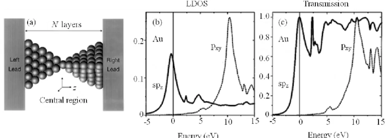
As described above, the conductivity of the metal atomic size contact is characterized by the formula (1). However, it is very difficult to determine the actual measurement of the transmission coefficient of each channel. There are three types of experimental methods for measuring the transmission coefficient such as a shot noise [34], conductivity fluctuation [35], superconducting multiple Andreev scattering [36, 37]. As a result, the monoatomic Au contact has a single channel with perfect transmission, while Nb has five channels but not perfectly transmitting. On the other hand, the conductivity and permeability coefficient are calculated for various metals by the first principles calculations and tight binding method [24, 38-41]. Fig. 1-12 exhibits the theoretical result for Au atomic contacts. Assuming the structure of the single atom contact of Au as shown in the Fig. 1-12(a), the Hamiltonian is determined based on the tight binding approximation and the local electronic density of states (LDOS) is also calculated in Fig.
1-12(b). The transmission coefficient is measured by using a nonequilibrium green function as in
Fig. 1-12(c). These results indicate that the LDOS at the central atom and the transmission
exhibit a resonance around the Fermi energy. In this case the charge neutrality condition pins the
Fermi energy at the center of the transmission resonance, provides the almost perfect
conductance quantization. Similar calculations are done for various metals like Al and Pb, it is
clear that the theoretical result agrees well with the experimental findings. However, some
results vary greatly depending on the contact structure assumed in calculation, it should be noted
that not all experimental results are reproduced.
1.3 Kondo effect in metallic nanoconstrictions
This subsection describes the historical background of the Kondo effect and the theoretical explanation of this effect in magnetic dilute systems. Finally, I will discuss how to detect the Fano resonance in several monatomic systems like a magnetic impurity atom adsorbed on nonmagnetic surface, which can be interpreted by the Kondo effect.
1.3.1 Background of the Kondo effect
Fig. 1-13 The resistance of gold at low temperature shows minima at around 3.7 K [42].
In 1934, the unexpected increase of resistance was experimentally observed in gold wires at low
temperature as shown in Fig. 1-13 [42]. Thirty years later, theorist J Kondo successfully
explained the upturn of resistance in his seminal work [43] as due to the scattering of the
conduction electrons with magnetic moments of impurity atoms present in the Au wires below a
characteristic temperature namely the Kondo temperature T
K. This explains that the shielding of
the impurity ions by conduction electrons is clarified after the formation of Kondo singlet state at
the lowest temperature. This phenomenon is commonly referred as Kondo effect. More generally,
the Kondo effect describes the electronic correlations between localized d electron moment and
sp itinerant electrons. When T
≧T
K, the spin exchange scattering is caused by the
antiferromagnetic exchange interaction of conduction electrons with the localized electrons. An
anti-rise with minimal value occurs. On the other hand, when T < T
K, localized spin is coupled
by the conduction electrons and the entire system will behave as a Fermi liquid at the sufficiently
1.3 Kondo effect in metallic nanoconstrictions
17
low temperature. At this time, the resistance value saturates to a constant value. This phenomenon is a many body correlation effect of conduction electrons to localized spins.
Historically this effect has been studied for a long time as one of the central tasks in condensed matter physics. The occurrence at low temperatures of resistivity minima in the dilute magnetic alloy having Cu with different concentration of Fe was first reported to be indicative of the similar observation of a minima in Au, as shown in Fig. 1-14(c) [44]. After that the Kondo effect was explored even in heavy electron systems where impurity atoms with a lattice structure are correlated with conduction electrons [45, 46]. From the beginning of last decades, the singlet Kondo state was directly observed in spectroscopic measurements for quantum dot systems and molecular devices [47-53].
In these above systems, the screening of the localized spin of this atom by the surrounding conduction electrons causes a sharp resonance close to the Fermi level at temperatures much less than the characteristic Kondo temperature T
K. Further, a detailed understanding of the Kondo effect in single atom contact of ferromagnetic and nearly ferromagnetic metal will be reported in chapter 3 and 4. In this chapter, I will first focus the examples of a dilute magnetic alloy system and explain the basic theory of Kondo effect. Later I will discuss the Kondo resonance as an example of monatomic Kondo system.
1.3.2 Magnetic impurities in metals
The schematic sketch of a dilute magnetic alloy system is illustrated in Fig. 1-14(a). When 3d transition metals are added as an impurity into the nonmagnetic metal host, the residual resistance of such a system is entirely different, shown in Fig. 1-14(b) [54]. In this case, the magnetic nature of the impurity may disappear depending on the type of the metal host and 3d metals. As an example, the resistance for two different dilute magnetic alloys of Cu and Au metal host with different concentration of Fe impurity shows minima at low temperature in Figs.
1-14(c) and (d) [44, 43]. In this subsection, we first explain the causes of generation and extinction of this impurity moment.
Let us suppose, a magnetic impurity having different valence from that of the host metal is
embedded in the metal. Fig. 1-15(a) represents the virtual bound state which is characterized by
the spatial distribution and by the energy spectrum of the impurity d electrons. Impurity d
electrons have an attractive potential from the nucleus and receive the centrifugal part of
potential l(l + 1)ħ
2/r
2derived from the angular momentum l and later form a barrier around the
impurity site. A brief representation of the impurity d electron energy level is depicted in Fig. 1-
15(b). The position of such energy level is determined by the attractive potential from the
nucleus. When the attractive potential is sufficiently large, the d electron level becomes lower
Chapter 1 Transport characteristics in metallic nanosystems
18
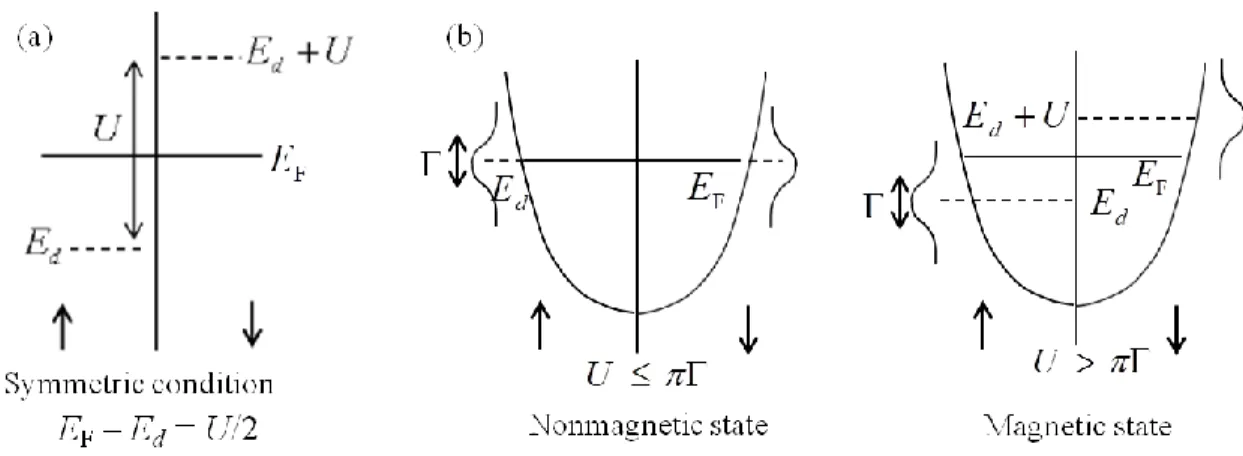
than the bottom of the conduction band as in state 1 of Fig. 1-15(b). In this state, the conduction electrons do not feel the presence of impurities and a stable eigenstate is formed. On the other hand, if it is very small, as in state 2 of Fig. 1-15(b), the d electron level is above the Fermi surface. In this case, trapping of electrons by the d electron level does not occur. If the potential is attractive between the state 1 and the state 2, the impurity d level is within the conduction band of the host metal as in state 3 of Fig. 1-15(b). Such state may nevertheless tend to localize the conduction electrons for a time in the vicinity of the impurity level. In this state, the average time an electron spends in the region of the impurity site increases, that can be understood by the uncertainty principle (Δε ~ h/Δt). Such an imperfect bound state is known as a virtual bound state (VBS) [55] because the wave functions become Bloch states far from the impurity.
Fig. 1-14 (Color online) (a) Schematic diagram of dilute magnetic alloy. (b) Based on Ga, the residual resistivity of 3d transition metal impurities in Al metal host is indicated by the value Δρ [54]. (c) The temperature dependence of resistance for dilute magnetic alloys of Cu with different concentration of Fe [44]. (d) Resistivity curves for the other dilute magnetic alloys AuFe at low temperature [43]. In both cases, the resistance upturn at the lowest temperature is accompanied by a logarithmic function.
1.3 Kondo effect in metallic nanoconstrictions
19
Fig. 1-15 (Color online) (a) Virtual trapped state of a metal-based impurity system. An energy barrier is formed by the contribution of the tensile and the centrifugal force potential. (b) Sketch of impurity potential of object in d electronic level. State 1, a constrained state, is located below the bottom of the conduction band. State 2 is on the Fermi surface which is unoccupied by the electrons. State 3 is present in the conduction band, forming a virtual bound state.
Fig. 1-16 The position of the impurity d electron level and the number of occupied electrons nd, the phase shift of conduction electrons on the Fermi surface δ(EF).
Conduction electrons having the same energy as the d electron level of this hypothetically bound state, the resonance is captured due to scattering and the phase of the wave function shifts by π/2. No phase shift will occur if the energy of conduction electrons is lower than d electron level but the phase shift will be π for the higher energy of conduction electrons. The phase shift of the electrons δ(E
F) on the Fermi surface, as shown in Fig. 1-16, is expressed by the number of electrons bound to the d level
EF
nd
(118)
In addition, the relation between the phase difference and the value of residual resistance at low
temperature is given by
Chapter 1 Transport characteristics in metallic nanosystems
20
F2 F
2 2 1 sin
/
4 l E
k e N N R c
e
res
(119) where N
eis the number of conduction electrons, N is the number of atoms, and c is the impurity atom density. The difference in residual resistance shown in Fig. 1-14(b) is that the heavier the atom, the larger the attractive potential of the nucleus and also explained that the d electron level and δ(E
F) are changed. The expression (118) is particularly important to derive the Kondo resonance level.
The electronic density of states of the VBS has a spread of the Lorentz function type as shown in Fig. 1-16. Anderson analytically derived a model which includes a sea of free electrons (that imitated a metal conduction band) and a finite number of localized d states (that related to the impurity atom). The interaction between them would obviously give rise to VBS-like hybridized states. In this model, the Hamiltonian using the creation and annihilation operator has the following form [56],
HHfreeHd HcoulombHmix
) 1 (
ˆ ˆ
V d c V c d
n N n U d d E c
c
E
dk k kd ke k d
d d k
k k k
(120) where k is the wave number of the conduction electron; σ is the spin direction (↑ or ↓); E
kand E
dare the energy of the conduction electron and the d electron, respectively;
ck,
ck,
dand
dare the creation and annihilation operator of conduction electrons and d electrons, respectively; U is the Coulomb repulsion between two electrons in the d level;
nˆd ddis the operator of the number of d electrons; V
kdis the hybridization term between d orbit and conduction band and N
eis the number of conduction electrons. In this equation (120), the first Hamiltonian represents the energy of conduction electrons, the second energy term for the d electrons, the third one is the Coulomb repulsion between d electrons and the last one is the hybridization term between d orbit and conduction band. The d orbit has five independent channels, but for simplicity it is represented here by a single d orbit.
For the Coulomb term, this Hamiltonian has a one-electron state
ck|0> and one-electron state in d level
d|0>. Therefore, if the Coulomb term is approximated to the mean field, it can be incorporated into the H
dterm.
d d
d E U n
E ˆ
![Fig. 1-2 (Color online) Representation of the Single atom contact fabrication using STM [14]](https://thumb-ap.123doks.com/thumbv2/123deta/9919057.1919950/14.918.211.713.203.468/fig-color-online-representation-single-contact-fabrication-using.webp)

![Fig. 1-10 Conductance histograms of rupture process of (a) Cu and (b) potassium (K) thin wires [29]](https://thumb-ap.123doks.com/thumbv2/123deta/9919057.1919950/24.918.114.799.118.346/fig-conductance-histograms-rupture-process-cu-potassium-wires.webp)
![Fig. 1-13 The resistance of gold at low temperature shows minima at around 3.7 K [42]](https://thumb-ap.123doks.com/thumbv2/123deta/9919057.1919950/26.918.126.796.347.659/fig-resistance-gold-low-temperature-shows-minima-k.webp)
![Fig. 1-14 (Color online) (a) Schematic diagram of dilute magnetic alloy. (b) Based on Ga, the residual resistivity of 3d transition metal impurities in Al metal host is indicated by the value Δρ [54]](https://thumb-ap.123doks.com/thumbv2/123deta/9919057.1919950/28.918.137.780.404.912/schematic-diagram-magnetic-residual-resistivity-transition-impurities-indicated.webp)

![Fig. 1-19 Spectral density of localized electrons calculated as a function of energy at various temperatures [65]](https://thumb-ap.123doks.com/thumbv2/123deta/9919057.1919950/35.918.299.603.120.400/spectral-density-localized-electrons-calculated-function-various-temperatures.webp)

