ヘリウムプラズマ照射を受けたモリブデン表面の
繊維状ナノ構造形成のための温度範囲の同定
Temperature Range for Fiber-Form Nanostructure Growth on Molybdenum Surface due to Helium Plasma Irradiation
髙村 秀一✝
Shuichi TAKAMURA
Abstract Nanostructure formation on molybdenum surface due to helium plasma exposure is investigated, focusing on the temperature band for fiber-form nanostructure growth. A precise temperature measurement can be obtained using thin thermocouples inserted into sheet specimens. The temperature range for nanostructure growth is determined to be 800 ~ 1050 K under the incident helium ion energy of 50 ~ 100 eV. The surface morphologies at around upper and lower boundary temperatures are different from a standard fiber-form nanostructure. The nano-fibers of molybdenum in a standard case was found to have a diameter of about 50 nm, while that of tungsten is a half of the molybdenum fibers.
1. Introduction
Since the discovery of fiber-form nanostructure on tungsten surfaces due to helium plasma irradiation 1),2),
many aspects have been investigated 3), focusing on the
the formation mechanism of such a fiber-form nanostructure4),5). The physical mechanism is not clear
so far although some modellings and MD simulations have been tried. Therefore, it is worthwhile from this point of view to study similar structures on another refractory metal surfaces, like molybdenum. The formation of fiber-form nanostructure on molybdenum has been confirmed 6),7), but not in detail.
Here, we focus on, first of all, a precise temperature range, over which the fiber-form nanostructure is formed on molybdenum surface, with use of thermocouples rather than radiation thermometers in order to exclude uncertainty of spectral emissivity. Secondly, the surface morphology of molybdenum at † Faculty of Engineering, AIT, Toyota 470-0392
the upper limit of surface temperature has been studied in terms of nanostructure formation and annihilation 8),9).
Finally, the difference of nanostructure between tungsten and molybdenum has been discussed.
2. Experimental Methods
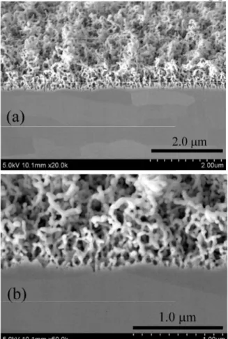
We employed two kinds of helium plasma exposure techniques for the nanostructure formation on molybdenum surfaces. One of them is shown in the insertion of Fig.1(a), without any external cooling stage. The target with the thickness of 1 mm was suspended with thermocouple sleeves with the diameter of 0.5 mm, which is inserted parallel to the molybdenum surface through the long hole. The nanostructure formation can be confirmed by a decrease in surface temperature due to an enhancement of black-body radiation from the target surface 8),10), and a visible check of black
molybdenum surface, as shown in Fig.1(a), where the thermocouple is R-type.
reflected intensity of a green laser light of 532 nm in wavelength is influenced by the surface morphology. The molybdenum sheet put on an indirectly cooled stage with a thin insulating mica sheet. K-type
thermocouple was inserted into molybdenum sheet. The stage was attached on the copper rod in the vacuum side. The opposite end of copper rod in the atmospheric side was cooled with circulating cooling water as shown in Fig.1(b-2).
Helium plasma exposures have been done in AIT-PID (Aichi Institute of Technology – Plasma Irradiation Device), where high density plasmas more than 1.0×10¹⁸ m-3 are produced with the bulk electron
temperature of 5 eV accompanied by energetic electrons whose apparent temperature is about 30 eV with a fraction of about 10 % 11). Before helium plasma
exposure argon plasma has been used to sputter surface contamination by biasing by -100 V for a few minutes.
3. Experimental Results and Discussions 3・1 Determination of Temperature Range
A typical temporal evolutions for the nanostructure growth on a molybdenum surface without any external cooling is shown in Fig.1(a). Just after an electrical biasing of the target (the ion incident energy is 80 eV), the temperature measured with R-type thermocouple shows 920 K. Then, a gradual decrease in temperature was associated by a surface blackening and a reduction in the ion saturation current due to a suppression of electron emission 12). The SEM image shown as one of
insertions in Fig.1(a) is very similar to that of nanostructured tungsten. Therefore, 920 K is well inside the temperature band for molybdenum nanostructure growth. Figure 2 shows other SEM showing the cross section, obtained with CP (Cross-sectional Polishing) method.
Similar technique has been used to determine the highest temperature which allows a nanostructure growth. The molybdenum temperature was raised up to about 1200 K and then decreased by decreasing the discharge current for plasma production every 10 minutes as shown in Fig.3. During every 10 minutes the plasma condition is kept constant, while any temperature changes are examined. Even a slight decrease in temperature means a development of nanostructure formation. We can determine the highest N S Cooling Water K - type Thermocouple Nd Magnet Diode - Pumped Solid - State Laser (532 nm) 115 Laser Light Mica Sheet Mo Target Target Stage Interference Filter (532 nm) Photodiode Detector Chamber Wall Vacuum Window
(b-1)
Cooling Liquid Copper ConductorSample Stage
K-type Thermocouple Vacuum Flange
Mica Sheet 100 mm
(b-2)
Fig.1 Exposure methods of molybdenum targets to helium plasmas: (a) without cooled stage. The target is suspended with R-type thermocouple of 0.5 mm in diameter of insulated sleeve. (b) with the stage attached on cooled copper rod of 95 mm in diameter, where (b-1) shows the laser light reflection for surface morphological change, and (b-2) shows the detail of sample stage with insulated mica sheet and K-type thermocouple.
temperature of 1050 K. When we kept the temperature at 1065 K for two hours, then we obtain neither
reduction in molybdenum temperature nor a blackening of its surface. From a series of experiments mentioned above, we can conclude that the highest temperature would be 1050 K. Another observation was obtained in the scheme of the molybdenum put on the indirectly
Figure 1 has already shown the nanostructure formation at T ~ 920 K. Laser light reflection method has also shown the formation at T ~ 870 K. So the temperature of 770 K was tried as shown in Fig.5(a). intensity of Fig.2 Typical nanostructure on Mo surface with oblique
view on the cross-section obtained with CP method. The ion energy Ei ~ 100 eV, T ~ 1000 K, the ion flux i ~ 1.2
×1020 m-2·s-1, and Fluence ~ 8.6×1024 m-2.
Fig.3 Determination of upper temperature limit for nanostructure formation by discriminating a self-cooling of target. The exposure method is the same as that in Fig.1(a). The surface temperature was controlled with the adjustment of discharge current. i ~ 1.8×10²¹ m-2·s-1 at T
~ 1050 K.
Fig.4 Determination of upper temperature limit for nanostructure formation by a change in laser light reflection. The final laser light reflection intensity is about 6.7 % of original one.
Fig.5 Determination of lower temperature limit for nanostructure formation by a reduction of laser light reflection: (a) T ~ 770 K, i ~ 2.4×10²¹ m-2·s-1, Fluence ~
2.2×1025 m-2 with E
i ~ 55 eV; (b) T ~830 K, i ~ 2.4×10²¹
m-2·s-1, Fluence ~ 2.3×1025 m-2 with E
cooled sample stage as shown in Fig.4, where the light reflection decreases down to 6.7 % of the starting reflected light intensity at 1045 K. Similar reduction was obtained at T ~ 1050 K, but a very small reduction was found at T ~ 1060K.
Figure 1 has already shown the nanostructure formation at T ~ 920 K. Laser light reflection method has also shown the formation at T ~ 870 K. So the temperature of 770 K was tried as shown in Fig.5(a). We have neither decrease in laser light reflection nor blackening of plasma-facing surface so that this temperature should be two low to have a growth of nanostructure. Some increase in surface temperature up to 830 K showed a complete suppression of laser light reflection as shown in Fig.5(b) so that this temperature is very close to the lowest value for the nanostructure formation.
3・2 Surface Morphology
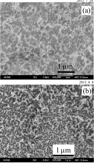
Around the highest temperature for nanostructure growth, the surface morphology is somewhat different from the standard fiber-form nanostructure shown in Fig.1(a). Figure 6 shows two examples: (a) at 1045 K and (b) at 1055 K. At this temperature range the fiber-form nanostructure formation and its plasma annealing 8),9) would proceed simultaneously. A detail
examination of Fig.6(a) reveals some traces of recovery caused by plasma annealing. Figure 6(b) shows an enhancement of recovery process. We can say that the morphological change is very sensitive to even a small difference in surface temperature. It seems that the nanostructure formation would be influenced by a viscosity of corresponding refractory metals 5) which
would have a similar temperature sensitivity, and that the critical temperature would have a flux dependency.
Figure 7 shows a comparison of nanostructure for molybdenum and tungsten. The diameter of nano-fibers of molybdenum is roughly twice as thick as that of tungsten.
4. Conclusions
A precise determination of temperature band for
fiber-form nanostructure has been done, using thermocouple rather than the employment of radiation thermometer which has an ambiguity of spectral emissivity of molybdenum surface. The maximum temperature for nanostructure growth is around 1050 K and the minimum one around 800 K under the incident ion energy of 50 ~100 eV. At the upper boundary temperature, nano-fibers growth competes with shrinkage due to plasma annealing. On the other hand the growth speed is very small at the lower boundary temperature. Although the temperature band of molybdenum for nanostructure growth is located just below that of tungsten, the phenomena are very similar. But the thickness of nano-fibers is larger for molybdenum than for tungsten.
2013_7_24
1 m
(a)
2013_8_81 m
(b)
Fig.6 Surface morphologies of He-defected molybdenum at around upper temperature limit; (a) T ~ 1045 K and (b)
T ~ 1055 K. For (a), i ~ 1.9×10²¹ m-2·s-1, Fluence ~ 1.4
×1025 m-2 at Ei ~ 65 eV, and (b) i ~ 2.3×10²¹ m-2·s-1, Fluence ~ 1.2×1025 m-2 at E
Acknowledgements
The research work was supported by Grant-in-Aid
for challenging Exploratory Research 23656578 from JSPS. The author would like to thank students in the plasma laboratory of AIT for their assistance.
References
1) S. Takamura, N. Ohno, D. Nishijima and S. Kajita, “Formation of Nanostructured Tungsten with Arborescent Shape due to Helium Plasma Irradiation”, Plasma Fusion Res. Vol.1, pp.051(2 pages), 2006. 2) M.J. Baldwin and D.P. Doerner, “Helium induced
nanoscopic morphology on tungsten under fusion relevant plasma conditions”, Nucl. Fusion Vol.48, pp.035001 (5 pages), 2008.
3) S. Takamura, S. Kajita and N. Ohno, “Nanostructure Formation on Refractory Metal Surfaces Irradiated by Helium Plasmas”, BUTSURI (Membership Journal of The Physical Society of Japan), Vol.68, pp.602-611, 2013 (in Japanese).
4) S.I. Krasheninnikov, “Viscoelastic model of tungsten ‘fuzz’ growth”, Phys. Scr. Vol.T145, 014040 (4pp), 2011. 5) R.D. Smirnov and S.I. Krasheninnikov, “On the shear strength of tungsten nano-structure with embedded helium”, Nucl. Fusion Vol.53, 082002 (4pp), 2013. 6) S. Kajita, W. Sakaguchi, N. Ohno N. Yoshida and T.
Saeki, “Formation process of tungsten nanostructure by the exposure to helium plasma under fusion relevant plasma conditions”, Nucl. Fusion Vol.49, 09005 (6pp), 2011.
7) S. Kajita, T. Saeki, Y. Hirahata and N. Ohno, “Formation of Metallic Nanostructure by Helium Plasma Irradiation”, Jpn. J. Appl. Phys. Vol.50, 01AH02 (4pp), 2011.
8) S. Takamura, T. Miyamoto, Y. Tomida, T. Minagawa and N. Ohno, “Investigation on the effect of temperature excursion on the helium defects of tungsten surface by using compact plasma device”, J. Nucl. Mater. Vol.415, S100-S103, 2011.
9) T. Miyamoto, S. Takamura and H. Kurishita, “Recovery of Tungsten Surface with Fiber-Form Nanostructure by Plasma Exposures”, Plasma Sci. Technol. Vol.15, pp.161-165, 2013.
10) S. Takamura, T. Miyamoto and N. Ohno, “Thermal radiation characteristics and direct evidence of tungsten cooling on the way to nanostructure formation on its surface”, J. Nucl. Mater. Vol.438, pp.S814-S817, 2013. 11) S. Takamura, “Characteristics of the Compact Plasma
Device AIT-PID with Multicusp Magnetic Confinement”, IEEJ Trans. Vol.7(S1), pp.S19-S24, 2012.
12) S. Takamura, T. Miyamoto and N. Ohno, “Effects of fiber-form nanostructures on particle emission from a tungsten surface in plasmas”, Nucl. Fusion Vol.52, pp.123001 (8pp), 2012.
(受理 平成26 年 3 月 19 日) Fig.7 Comparison of nano-fibers between (a)