INVITED PAPER
Special Section on Electronic DisplaysAl-Based Metal Mesh Electrodes for Advanced Touch Screen Panels Using Aluminum Nitride System Optical Absorption Layer
Mototaka OCHI†a), Yoko SHIDA†, Hiroyuki OKUNO††, Hiroshi GOTO†, Toshihiro KUGIMIYA†, andMoriyoshi KANAMARU††,Nonmembers
SUMMARY An Al-N system optical absorption layer has been devel- oped, to be used for Al-based metal mesh electrodes on touch screen panels.
The triple-layered electrode effectively suppresses the optical reflection in both visible light and the blue color region and exhibits excellent wet etch- ing property that accommodates micro-fabrication. Due to its high noise immunity and contact sensitivity originating from its low electrical resis- tivity, the proposed metal mesh electrodes are useful for touch-sensitive panels in the next generation ultra-high-resolution displays.
key words:touch screen panel, metal mesh electrode, projected capacitive, invisible, etching property
1. Introduction
The market of touch screen panels has grown rapidly due to the popularity of smart phones and tablet PCs equipped with high-definition displays[1]. There are various types of touch panels available on the market, the features of which depend on the touch controlling detection methods[2]. Pro- jected capacitive type touch sensors are the current main- stream because they are highly precise and respond to multi- touching (multipoint detecting). Recently, one glass solu- tion (OGS), in-cell, and on-cell touch technologies using projected capacitive type touch sensors are also drawing in- creasing attention due to their ability to reduce the weight, thickness and cost of the touch devices[3]–[5].
In the projected capacitive type touch sensors, the elec- trodes are composed of two parts; one is located in the frame area and the other is in the sensor area. The electrodes for the frame area generally have a stacked structure with two or three metal elements such as Mo-Nb/Al-Nd/Mo-Nb or Mo/Al/Mo. As for the sensor area, Sn-doped indium ox- ide (ITO) electrodes are widely used to detect finger touch.
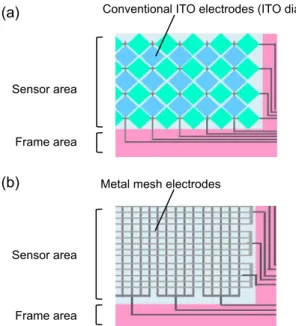
However, further improvements in their noise immunity and contact sensitivity are required in order to apply the touch sensors to ultra-high resolution displays such as those of more than 500ppi. For the conventional ITO electrodes as shown in Fig. 1 (a), the metal mesh electrodes as shown in Fig. 1 (b) are recognized as an alternative option to meet the requirements. The resistivity of metal mesh electrodes is generally two or more orders of magnitude lower than that
Manuscript received February 23, 2015.
Manuscript revised June 1, 2015.
†The authors are with Kobe Steel Ltd., Kobe-shi, 651–2271 Japan.
††The authors are with Kobelco Research Institute Inc., Kobe- shi, 651–2271 Japan..
a) E-mail: [email protected] DOI: 10.1587/transele.E98.C.1000
of the ITO electrodes, which allows sufficient noise process- ing and high clock frequencies according to the decrease of the decay time constant. Furthermore, the structure has an advantage regarding utilization of the fringe capacitance[6], which leads to improvement of the contact sensitivity.
Cu-based mesh electrodes have been proposed. How- ever, the single layer mesh electrodes have a drawback in the external light reflection, and both invisible and micro- patterning technique for the multi-layered Cu-based mesh electrodes are yet to be established at the moment.
Al-N system optical absorption layer has been devel- oped, to be used in Al-based triple-layered metal mesh elec- trodes for touch screen panels. The optical absorption layer is fabricated by the sputtering, photolithography and wet- etching processes that are already common in the FPD in- dustry. The Al-based mesh electrode is one of the promising technologies not only to overcome poor display characteris- tics in the amount of incident lighting environment from the outside of the display device, but also to meet the require- ments of micro-fabrication.
2. Concept of Al-Based Mesh Electrodes
The characteristics of mesh electrodes (sensing electrodes)
Fig. 1 Touch sensor of electrode structure by (a) conventional ITO electrodes and (b) metal mesh electrodes.
Copyright c2015 The Institute of Electronics, Information and Communication Engineers
Fig. 2 Proposed Al-based triple-layered metal mesh electrodes.
are evaluated in terms of their resistivity, reflectivity and micro-patterning property. Conventionally, to suppress the reflectance of the electrode surface, three or more optical adjustment layers are adapted on the corrosion resistive in- terconnection such as a three layered interconnection con- sisting of Mo-Nb/Al-Nd/Mo-Nb or Mo/Al/Mo for control- ling the optical interferences at the interfaces. The structure obviously requires six or more layers in total, often resulting in poorer production yield and higher production costs.
To overcome these problems, a different structure, that is, an Al-based triple-layered structure was applied. Figure 2 shows the structure of the proposed mesh electrodes. To re- duce the number of the optical adjustment layers, a single optical absorption layer and a single high refractive index layer are utilized. Then corrosion-resistive Al alloy thin film such as Al-Mn alloy is employed for the interconnection. In the present study, a double-layered structure with the trans- parent conductive oxide (TCO) thin film (with a high reflec- tion index) and the Al-N system thin film (with a high op- tical absorption factor) are adapted. The Al-N system thin film was fabricated by nitridation of aluminum because the reaction control by sputtering is simpler than oxidation and also wet etching of the nitride films is easier.
3. Experimental
3.1 Sample Preparation
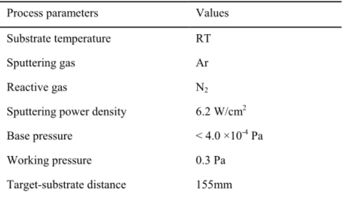
The Al-N system thin films were deposited on glass sub- strates (Corning 1737) by reactive DC magnetron sputter- ing with various gas compositions of argon and nitrogen for evaluation of the characteristics as the optical absorp- tion layer. The pure Al and Al-based sputtering targets were prepared for deposition. The sputtering process parameters are listed in Table 1.
For the evaluation of the characteristics as the metal mesh electrodes, the stacked thin films were fabricated by continuous deposition of the Al alloy thin film (250 nm), the Al-N system thin film (50 nm) and the transparent con- ductive oxide (TCO) thin film (50 nm) in turn.
After the deposition, the stacked thin films were
Table 1 Sputtering process parameters for Al-N system thin films.
cleaned by a deionized (DI) water rinse, followed by a high- purity N2blow dry. Then, the photoresist (AZ TFP 650) was coated on the stacked thin films and the exposed photore- sist was removed using the developer (AZ 300 MIF). After that, wet-etching was conducted by immersion into the con- ventional PAN acid etchant (a mixture of H3PO4, HNO3, CH3COOH and H2O with a volume ratio of 70 : 2 : 10 : 18) at 40◦C. Finally, the remaining photoresist was removed from the substrate by immersing it in photoresist stripper (TOK104) at 80◦C.
3.2 Characterization
In order to characterize the Al-N system thin films, optical, electrical and structural analyses were conducted. The spec- tral reflectance and transmittance of the Al-N system thin films were measured using an automatic absolute reflectance analyzer (ARM-500N manufactured by Jasco Corp.) in the range between 250 and 850 nm. The resistivity of the Al- N system thin films was measured by a four-point probe (Milliohm HiTester produced by Hioki Corp.). The temper- ature dependence of the film resistivity was measured using the test key, which has small ohmic electrodes on the four corners of the Al-N system thin films[7]. Some samples were examined by Hall effect measurements using the same test key[8],[9](Resitest 8300 produced by Toyo Corp.).
The structural properties of the Al-N system thin films were analyzed by X-Ray diffraction (XRD) (SmartLab pro- duced by Rigaku Corp.) with a graphite monochromatized Cu Kα (λ = 1.54056Å) source in θ-2θ scanning mode.
Structural observation was also carried out using a field- emission high-resolution transmission electron microscope (FE-HRTEM) for phase-contrast imaging and selected-area electron diffraction (SAED) for crystallographic informa- tion (HF2200 produced by Hitachi Corp.). Then, X-ray pho- toelectron spectroscopy (XPS) (Quantera SXM produced by Physical Electronics Corp.) was also carried out to inves- tigate the associated chemical bonding states of the Al-N system thin films. The source of the photoelectron excita- tion was monochromated Al Kα(hν=1486.6 eV) radiation which had a 100-µm-diameter spot on the sample surface.
The spectral reflectance of the Al-based triple-layered stack thin films was measured using the automatic absolute
reflectance analyzer. The resistivity of the Al-based triple- layered stack thin films was measured by the same four- point probe in the method used for the Al-N system thin films. The evaluation of the mesh electrodes from the view point of the micro-fabrication, the shape of the etched sur- face and cross-section was observed by an optical micro- scope (OM) and a cross-sectional scanning electron micro- scope (SEM).
4. Results and Discussion
4.1 Properties of Optical Absorption Layers
4.1.1 Optical Properties of the Al-N System Thin Film Figure 3 shows the reflectance, the transmittance and the absorptance of the 50-nm-thick Al-N system thin films (λ= 550nm) as a function of the nitrogen flow ratio during the DC magnetron sputtering. These plots were extracted from the spectral reflectance and the spectral transmittance. The results obtained from the thin film deposited without nitro- gen gas (flow ratio of 0%, Ar gas only) are also given as a reference. The reflectance of the Al-N system thin films was varied between 20.8 and 90.5% at 550 nm, depending on the nitrogen flow ratio. The reflectance of the Al-N system thin films was decreased as the nitrogen flow ratio increased and kept to a substantial constant beyond the nitrogen flow ratio of approximately 23%. In contrast, the transmittance was increased with the nitrogen flow ratio and changed from 0.1 to 78.1% at 550 nm. The transmittance was large (>76.5%) and nearly constant in the higher nitrogen flow retio region (>23.8%).
It is noted that the transmittance rapidly increased as the nitrogen flow ratio became greater than 16.7%. The ab- sorptance of the Al-N system thin films, characterized by a
Fig. 3 Reflectance, transmittance and absorptance of Al-N system thin film deposited under various nitrogen flow ratio with pure-Al sputtering target. Absorptance Abs(λ) was defined as; Abs(λ)=100%−R(λ)−T(λ), where R(λ) is reflectance and T(λ) is transmittance at each wavelength (λ).
balance of the reflectance and transmittance, was calculated from the reflectance and the transmittance as shown in Fig. 3 The absorptance of the Al-N system thin films takes its max- imum value at a nitrogen flow ratio of 16.7%. Also, it was found from the result that the absorptance decreases along with the abrupt increase in transmittance as the further ni- trogen flow ratio was increased. This trend was commonly observed in all wavelengths on the visible light region.
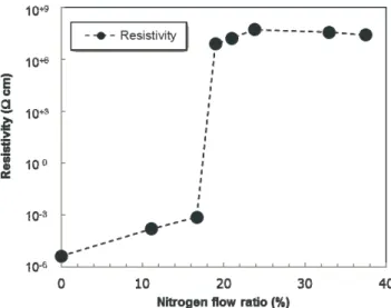
4.1.2 Electrical Properties of Al-N System Thin Film Figure 4 shows the electrical resistivity of the 50-nm-thick Al-N system thin films at different nitrogen flow ratios, cor- responding to the optical properties shown in Fig. 3. The electrical resistivity increased gradually as the nitrogen flow ratio increased and rapidly increased when the nitrogen flow ratio became greater than 16.7%, which was similar behav- ior as that for the transmittance. This result indicates that the characteristics of the Al-N system thin films were changed easily from a conducting nature to an insulating nature de- pending on the amount of the nitrogen during the sputtering.
The electrical resistivity of the Al-N system thin film (showing its highly optical absorption nature), which was deposited with a nitrogen flow ratio of 16.7%, was about 7.5×10⁻⁴Ω·cm. The value was approximately two orders of magnitude higher compared with that of the pure Al thin film; however, it was found that the resistivity of the films maintained a sufficiently low compared with that of the insu- lating Al-N system thin film. The temperature dependence of the electrical resistivity of the Al-N system thin film with a highly optical absorption nature was also investigated in the temperature range between 80 and 370K. As the mea- surement temperature was increased, the resistivity of the film decreased monotonically as shown in Fig. 5. The carrier density of the film estimated by Hall-effect measurements using the same test-key was about 7.0×1022cm−3at 300K and slightly increased with temperature. These results sug-
Fig. 4 Electrical resistivity of Al-N system thin film deposited under various nitrogen flow ratio with pure-Al sputtering target.
Fig. 5 Temperature dependence of the Al-N thin film deposited on the nitrogen flow ratio of 16.7% having the high optical absorption nature and the high electrical conductivity. Resistivity was measured using test key which was fabricated small ohmic electrodes on the four corners of Al-N system thin films.
Fig. 6 XRD diagrams of Al-N system thin films deposited under different nitrogen flow ratio with pure-Al sputtering target.
gest that although the Al-N system thin film with a highly optical absorption nature possessed a high carrier density of over 1022cm−3, the behavior is not likely to be one expected from the general metallic thin films (rather semiconductor- like properties).
4.1.3 Structural Properties of Al-N System Thin Film Figure 6 shows the X-ray diffraction patterns from the 50-nm-thick Al-N system thin films deposited with vari- ous nitrogen flow ratios. The pure Al thin film, which was deposited without nitrogen gas addition, exhibits crys- talline aluminum with clear peaks corresponding to (111),
(200), (220) and (311) plane. In the case of 16.7% ni- trogen addition, the peaks relative to the crystalline alu- minum completely disappeared and only the broad band from glass substrates was observed. In the case of 23.8%, the crystalline aluminum nitride (AlN) peaks corresponding to (100), (002), (101), (102), (110), (103) and (112) plane were generated. As for 33.3%, the peak intensity increases with the nitrogen flow ratio.
In the thin film deposited with 16.7% nitrogen addi- tion, the Al-N system thin film has a highly optical absorp- tion nature. However, the XRD peaks are not observed in the Al-N system thin film. Thus, we further characterized the thin film by means of HRTEM imaging. In Fig. 7 (a), an in-plane HRTEM image of the Al-N system thin film (16.7% nitrogen flow ratio) shows that some fine microcrys- tals were involved in the dominant amorphous material. The mostly crystallite sizes are estimated to be 5 nm or less. The SAED patterns taken from the cross-section HRTEM speci- mens are shown in the inset of Fig. 7 (a). All diffraction rings correspond to the hexagonal AlN. From this fact, it is con- sidered that the crystalline nature is oriented from the AlN phase, not the Al phase, and the AlN is partially crystallized.
On the other hand, as shown in Fig. 7 (b), AlN crystals were observed in the entire in-plane HRTEM image of the Al-N system thin film with 33.3% nitrogen flow ratio. The crys- tallite sizes are more than about 5 nm and the SAED patterns show clear diffraction rings as shown in Fig. 7 (b).
Figure 8 shows the XPS narrow scan spectrum for Al2p from the thin films. The spectrum for 16.7% can be divided into two components. It is thought that the peak at the higher binding energy (close to 74.4 eV) is related to the Al-N bond and the shoulder at lower binding energy (close to 72.8 eV) is originated from an aluminum metal. In the case of the Al- N system thin film with 33.3% nitrogen flow ratio, only the peak at higher binding energy (close to 74.4 eV) is observed.
Therefore, in the Al-N system thin film with the highly opti- cal absorption and conductivity nature, which was deposited on the nitrogen flow ratio of 16.7%, it is found that there is structural change, from the crystalline aluminum states to the amorphous states including Al-N bond. In general, the AlN thin films are transparent (wideband gap) insulat- ing films[10], [11]. Therefore, it is likely that the amor- phous AlN including the fine AlN microcrystalline textures contribute markedly to the optical absorption. On the other hand, the aluminum component with unattached Al-N bond could contribute to the conductivity. These characteristics were achieved by the optimized nitrogen content in the Al- N system thin film.
4.1.4 Effects of Additive Element
In order to improve the process robustness of the Al-N sys- tem thin film during the sputtering process, an Al alloy sput- tering target with transition metal was developed. Figure 9 shows typical optical and electrical characteristics of the Al- N system thin films (new Al-N system thin film) deposited using the Al alloy sputtering target. There are various re-
Fig. 7 In-plane HRTEM images of Al-N system thin film deposited in nitrogen flow ratio of (a) 16.7%
and (b) 33.3%, respectively. The insets show the SAED patterns and analysis result. The SAED patterns are indexed based on the AlN hexagonal (a=b=3.11 Å,α=β=90◦,γ=120◦). In Fig. 7 (a), the measured spacing of the crystal plane indices (100), (101) and (110) is 2.64 Å, 2.33 Å and 1.53 Å, respectively. In Fig. 7 (b), the measured spacing of the crystal plane indices (100), (002), (101), (102), (110), (103) and (200) is 2.74 Å, 2.51 Å, 2.41 Å, 1.85 Å, 1.58 Å, 1.43 Å and 1.34 Å, respectively.
Fig. 8 XPS narrow scan spectra in Al 2p on the surface of Al-N system thin film deposited under nitrogen flow ratio of (a) 16.7% and (b) 33.3%.
ports regarding the effect of the additive element on the amorphous AlN thin film[12]–[15]. In this case, it turned out that the new Al-N system thin films give a broader pro- cess margin in terms of the nitrogen flow ratio during sput- tering than the Al-N system thin films deposited using the pure-Al sputtering target as is evident from Figs. 3 and 4.
Fig. 9 Reflectance for optical property and electrical resistivity for elec- trical property of new Al-N system thin film deposited under various nitro- gen flow ratio with Al alloy sputtering target.
4.2 Al-Based Mesh Electrode Properties
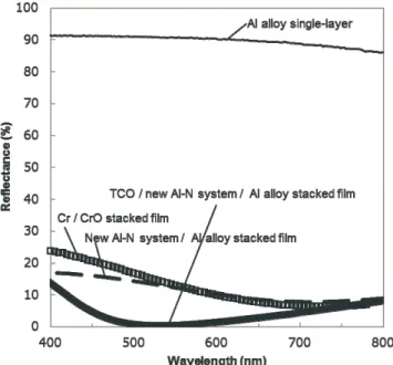
Figure 10 shows the reflectance spectra of the various struc- tures for the Al-based metal mesh electrodes; (a) the Al al- loy single-layer (corrosion resistant Al alloy (250 nm) thin film on a glass substrate), (b) the double-layered structure
Fig. 10 Reflectance spectra; (a) Al alloy single-layer, (b) new Al-N sys- tem/Al alloy stack film, (c) TCO/new Al-N system/Al alloy stack film and (d) black matrix stack film (Cr/CrO).
(new Al-N system (50 nm)/Al alloy (250 nm) stacked film on glass), (c) the triple-layered structure (TCO (50 nm)/new Al-N system (50 nm)/Al alloy (250 nm) stacked film on glass) and (d) the reference (Cr/CrO stacked film that is widely used as a black matrix on glass). Here, the new Al- N system thin film was adapted, which was optimized to have a high optical absorption nature and a high electrical conductivity, as discussed above and adapted to the optical absorption layer. As shown in Fig. 10, the reflectance of the double-layered structure (b) is markedly low compared with that of the Al alloy single-layer (a) and equivalent to that of the reference stacked film (d) used as a black ma- trix. The optical characteristics were further improved by stacking the TCO films with the refractive index at 550 nm of about 2.13. Note that the TCO thin film was selected be- cause of its large difference in refractive index, as well as in consideration of the etching properties. This result indi- cates that the proposed triple-layered structure can be easily controlled to have sufficiently low reflectance in the visible light region and the blue color region on the surface[16](re- quested from the visibility in the display). The resistivity of the triple-layered structure (c) is only about 1.2 times larger compared with that of the 1st layer of the Al alloy thin film since the ohmic contact between the each layer is estimated by the Kelvin pattern[17]. It means that the triple-layered metal mesh electrodes can maintain a sufficient advantage compared to the ITO electrodes even if the aperture ratio reaches about 90% although the Al alloy thin film has a lit- tle bit higher resistivity of 14.0µΩ·cm than pure Al.
Finally, the Al-based triple-layered metal mesh elec- trodes were completed by micro-patterning using the mesh with TCO/new Al-N system/Al alloy stack film. Wet- etching process with the conventional PAN etchant (mix-
Fig. 11 (a) OM image and (b) SEM image of Al-based triple-layered mesh electrodes.
ture of phosphoric, acetic and nitric acid, frequently used in the TFT manufacturing process[18]). Figures 11 (a) and (b) show the OM image and the SEM image, respectively. It was found that the Al based triple-layered metal mesh elec- trode is capable of forming a fine pattern less than below 5µm in width without causing an electrical corrosion due to the employment of the corrosion resistant Al alloy.
5. Conclusion
An Al-N system optical absorption layer was successfully developed for the Al-based metal mesh electrodes in touch screen panels. The obtained results were as follows; 1) the amorphous AlN including the fine AlN microcrystalline textures contributes enormously to the optical absorption.
2) The aluminum component with unattached Al-N bond could contribute to the conductivity. These characteristics were achieved by the optimized nitrogen content in the Al- N system thin film. Further, we have developed the Al al- loy sputtering target in to improve the process robustness of the Al-N system thin film during the sputtering process.
The triple-layered electrodes effectively suppressed the op- tical reflection in both visible light and blue color region and exhibited excellent wet etching property that accommo- dates to the micro-fabrication. It is concluded that due to its high noise immunity and contact sensitivity originating
from its low electrical resistivity, the proposed metal mesh electrodes are useful for touch-sensitive panels in next gen- eration ultra-high-resolution displays.
This technology can be applied to not only the metal mesh electrode, but also the bridge electrode for the conven- tional touch-detection method. Besides, the reversed triple- layered structure based on this technology can also be ex- tended to both the metal mesh electrode and the bridge elec- trode for the OGS-type touch screen device.
References
[1] 25th Display Search Forum, 2013 Touch Panel Market Analysis.
[2] Y. Mitani and K. Nakatani, “Feature and technology trends of var- ious touch panels,” NIPPON GOMU KYOKAISHI, vol.84, no.8, pp.256–266, 2011 (in Japanese).
[3] N. Nakatani, “New technology trends in touch panel sensing,” Proc.
IDW ’12, pp.807–810, 2012.
[4] H. Haga, J. Yanase, Y. Nonaka, D. Sugimoto, K. Takatori, and H.
Asada, “A 10.4-in. on-cell touch-panel LCD with correlated noise- subtraction method,” SID Symposium Digest of Technical Papers, vol.43, no.1, pp.489–492, 2012.
[5] S. Takahashi, D.H. Cho, H.-S. Moon, and N.D. Kim, “In-cell embed- ded touch screen technology for large size LCD applications,” SID Symposium Digest of Technical Papers, vol.41, no.1, pp.544–547, 2010.
[6] R. Hattori, “Touch panel saizensen 2013–2014,” NIKKEI ELEC- TRONICS, pp.40–49, 2012 (in Japanese).
[7] M. Ochi, S. Morita, Y. Takanashi, H. Tao, H. Goto, T. Kugimiya, and M. Kanamaru, “High reliability of back channel etch-type TFTs using new oxide semiconducting material,” Proc. IDW ’13, pp.371, 2013.
[8] L.J. Pan Der Pauw, “A method of measuring specific resistivity and hall effect of discs of arbitrary shape,” Philips Res. Rep., 13, pp.1–9, 1958.
[9] L.J. Pan Der Pauw, “A method of measuring the resistivity and hall coefficient on lamellae of arbitrary shape,” Philips Tech. Rev., 20, pp.220–224, 1959.
[10] J.M. Khoshman and M.E. Kordesch, “Optical characterization of sputtered amorphous aluminum nitride thin film by spectroscopic ellipsometry,” Journal of Non-Crystalline Solids, vol.351, no.40-42, pp.3334–3340, 2005.
[11] H.-Y. Joo, H.J. Kim, S.J. Kim, and S.Y. Kim, “Spectrophotometric analysis of aluminum nitride thin films,” Journal of Vacuum Science
& Technology A, vol.17, no.3, pp.862–870, 1999.
[12] H. Chen, K. Chen, D.A. Drabold, and M.E. Kordesch, “Band gap engineering in amorphous AlxGa1−xN: Experiment andabinitio cal- culations,” Appl. Phys. Lett., vol.77, no.8, pp.1117–1119, 2000.
[13] K. Gurumurugan, H. Chen, and G.R. Harp, W.M. Jadwisienczak, and H.J. Lozykowski, “Visible cathodoluminescence of Er-doped amorphous AlN thin film,” Appl. Phys. Lett., vol.74, no.20, pp.3008–3010, 2000.
[14] W.M. Jadwiseienczak, H.J. Lozykowski, F. Perjeru, H. Chen, M.
Kordesch, and I.G. Brown, “Luminescence of Tb ions implanted into amorphous AlN thin films grown by sputtering,” Appl. Phys. Lett., vol.76, no.23, pp.3376–3378, 2000.
[15] M.L. Caldwell, A.L. Martin, C.M. Sparlding, P.G. Van Patten, M.E.
Kordesch, and H.H. Richardson, “ Visible emission from thin-film phosphors of amorphous AlN:Cu, Mn, and Cr,” Proc. MRS, vol.639, Symoosium G, 2000.
[16] T. Smith and J. Guild, “The C.I.E. colorimetric standards and their use,” Transactions of the Optical Society, vol.33, no.3, 1931.
[17] W.M. Loh, S.E. Swirhun, E. Crabbe, K. Saraswat, and R.M.
Swanson, “An accurate method to extract specific contact resistiv- ity using cross-bridge Kelvin resistors,” IEEE Electron Device Lett.,
vol.6, no.9, pp.441–443, 1985.
[18] T. Tsujimura and A. Makita, “Molybdenum/aluminum stacked metal taper etching for high-resolution thin-film transistor liquid- crystal display,” Journal of Vacuum Science & Technology B, vol.20, no.5, pp.1907–1913, 2002.
Mototaka Ochi received the B.S. and M.S. degrees in Electronic Engineering from Okayama University, Japan, in 1998 and 2000, respectively. He is a senior researcher of Elec- tronics research laboratory at Kobe Steel Ltd.
He is currently engaged in the development of thin film material for flat panel displays.
Yoko Shida received the B.S. degree in Material Engineering from National Institute of Technology, Tsuruoka College and M.S. degree received in Material Chemistry in Tsukuba Uni- versity, Japan, in 2006 and 2008, respectively.
She is researcher of Electronics research labora- tory at Kobe Steel Ltd. She is currently engaged in the development of thin film material for flat panel displays.
Hiroyuki Okuno received the B.S. and M.S.
degrees in applied chemistry from Yamaguchi University, Japan, in 1999 and 2001, respec- tively. He is a senior engineer of Technical En- gineering Department at Kobelco Research In- stitute, INC. He is currently engaged in the de- velopment of sputtering target material and thin film material for flat panel displays.
Hiroshi Goto received the B.S. and M.S. de- grees in Material Engineering from Hiroshima University, Japan, in 1994 and 1996, respec- tively. He is a senior researcher of Electronics research laboratory at Kobe Steel Ltd. He is cur- rently engaged in the development of thin film material for flat panel displays.
Toshihiro Kugimiya received the B.S., M.S.
and Dr. degrees in electronics engineering from Toyohashi University of Technology in 1991, 1993, and 2011, respectively. In 1993, he joined Kobe Steel, Ltd., Japan, and he has worked on metal interconnections for FPD, especially, Al- alloy film interconnections. Since 2009 when he joined a project for oxide semiconductor for FPD in Electronics Research Lab. in Kobe Steel, he has directed the research of Oxide-TFT fab- rication process and analyses of Oxide materials and TFTs.
Moriyoshi Kanamaru received the B.S.
and M.S. degrees in Nuclear Engineering from Osaka University, Japan, in 1982 and 1985, respectively and Dr. degrees in nature science from Stuttgart Universitaet, in Germany, in 1994. He is a general manager of Technical En- gineering Department at Kobelco Research In- stitute, INC. He is currently engaged in sput- tering target materials mainly for flat panel dis- plays.