Title Effects of Potential Modulations on Optical Gain Properties inInGaN-based Green Laser Diodes( Dissertation_全文 )
Author(s) Kim, Yoon Seok
Citation Kyoto University (京都大学)
Issue Date 2014-03-24
URL http://dx.doi.org/10.14989/doctor.k18281
Right 許諾条件により本文は2014-10-01に公開
Type Thesis or Dissertation
Textversion ETD
Effects of Potential Modulations on Optical Gain Properties
in InGaN-based Green Laser Diodes
Yoon Seok Kim
2014
Effects of Potential Modulations on Optical Gain Properties
in InGaN-based Green Laser Diodes
Table of contents
Preface ··· 1
Chapter 1. Introduction
1.1 Research background- Historical stories of green laser diodes ··· 51.2 Research background- Physical obstacles forward green laser diodes ··· 6
1.3 Construction of this thesis ··· 8
Chapter 2. Theoretical Background and Literature Survey
2.1 Potential modulations ··· 132.1.1 Potential fluctuation: in-plane modulation ··· 14
2.1.2 Internal electric field: out-of plane modulation · ··· 16
2.1.2.1 Spontaneous polarization, Psp ··· 16
2.1.2.2 Piezoelectric polarization, Ppz ··· 17
2.1.2.3 Crystal angle dependence of internal electric field ··· 20
2.2 Optical gain··· 24
2.2.1 Formula of gain contributed by material parameters ··· 24
2.2.2. In-plane potential modulation ··· 25
2.3 Summary ··· 27
Chapter 3. Carrier Dynamics and Nanoscopic Optical Properties
of Polar (0001) Green InGaN QWs
3.1 Introduction ··· 293.2 Experiments ··· 30
3.2.1 Macroscopic optical measurement system ··· 31
3.3 Fundamental optical properties ··· 34
3.3.1 Inhomogeneous broadening ··· 34
3.3.2 Exciton/Carrier dynamics ··· 37
3.3.3 In composition and well width · ··· 38
3.4 Summary ··· 40
Chapter 4. Optical Gain Properties
of Polar (0001) Green InGaN Laser Diodes
4.1 Optical mode gain ··· 434.1.1 Stimulated emission by optical pumping ··· 43
4.1.2 Spontaneous and stimulated emission spectra ··· 45
4.1.3 Hakki and Paoli’s scheme ··· 46
4.1.4 Injection current density dependent mode gain ··· 48
4.1.5 Fitting results of gain spectra and inhomogeneous broadenings ···49
4.2 Peak energy comparison as functions of current density and carrier density ··· 54
4.3 Summary ··· 56
Chapter 5. Carrier Dynamics and Nanoscopic Optical Properties
of Semipolar
{
20
2
1
}
Green InGaN QWs
5.1 Introduction ··· 595.2 Experiments ··· 60
5.3 Results and discussions ··· 61
5.4 Summary ··· 69
Chapter 6. Optical Gain Properties
of Semipolar
{
20
2
1
}
Green InGaN Laser Diodes
6.1 Introduction ··· 736.2 Experiments ··· 74
6.2.1 Gain measurement under pulsed operation ··· 74
6.3 Lasing property and the current dependent optical mode gain ··· 76
6.4 Gain suppression and carrier density dependence of EL and gain peak energy ··· 79
6.6 Summary ··· 87
Chapter 7. General Summary
7.1 Introduction ··· 917.2 Summary of each chapter ··· 91
7.2.1 Summary of chapter 2 ··· 91
7.2.2 Summary of chapter 3 ··· 92
7.2.3 Summary of chapter 4 ··· 92
7.2.4 Summary of chapter 5 ··· 93
7.2.5 Summary of chapter 6 ··· 93
7.3 Future prospective of green laser diodes ··· 94
7.3.1 Green LDs on polar (0001) plane ··· 94
7.3.2 Green LDs on semipolar planes ··· 94
Acknowledgement
971
Preface
In recent times, the demand for green laser diodes (LDs) has increased remarkably due to their use in several applications such as full color display, medical applications, and anti-piracy systems (APS). Up until 2008, it was difficult to fabricate green laser diodes using III-nitrides since their threshold current densities increase significantly due to strain induced piezoelectric polarization and inhomogeneous broadening (σ) by tail states in the InGaN layer. Pure green LDs grown on semipolar {2021} GaN substrates were demonstrated by Sumitomo electric industry for the first time in 2009. This was followed by the fabrication of 515 nm green LDs grown on polar (0001) planes by Nichia Corporation. Then, several groups with slightly varying approaches succeeded in developing green LDs on the polar (0001). The success of green LDs based on the semipolar substrates is due to the reduced internal electric fields for their crystal angles. On the other hand, epitaxial improvement played a key role for the (0001) LDs because high internal electric fields are inevitable in the polar (0001) system.
Here we provide a brief summary of this thesis and its structure. In Chapter 2, a theoretical understanding of the physical limitations of III-nitrides light emitters such as internal electric field and inhomogeneity is developed. The chapter also discusses gain formation and the effects of material parameters on the gain. There are several factors contributing to the optical gain, such as dipole transition moment, the square of the overlap integral, effective mass and line width function. The dipole transition moment is of particular importance in semipolar or nonpolar systems due to the anisotropic character of the valence bands. Since the square of the overlap integral is associated with the tilted crystal angle, the semipolar or nonpolar systems benefit from a higher overlap integral. The effective mass, which is related to the density of states (DOS), can be smaller for semipolar/nonpolar systems due to their smaller DOS. This contributes towards population inversion in these systems.
In Chapter 3, nanoscopic PL mapping results of LD structures on the polar (0001) planes are compared with conventional green emitting QWs grown on epitaxially laterally overgrown GaN (ELOG) templates. The green LD structure shows improved in-plane uniformity, such that the wavelength distribution is as small as 2 nm in comparison to the
2
conventional green QW with distributions larger than 20 nm. Furthermore the intensity distribution in this LD structure is also superior to conventional QWs. Comparing PL temperature dependence and calculation further supports above homogeneity with σ of 25 meV while conventional one reveals 180 meV. As confirmed by carrier recombination lifetime (τ) measured by time resolved PL, the overlap integral of these LD structure is about 2.1 times higher than that of the conventional QWs. From this finding, the In composition and InGaN thickness are evaluated to be 28% and 2.5 nm, respectively. Compared with the conventional QW, a thinner InGaN QW with a higher In composition is used in the current green LDs.
In Chapter 4, results of the optical gain measurements are discussed. The internal loss of the green LD on the polar (0001) plane is estimated to be ~10 cm-1. Owing to the improvement in epitaxy, this is significantly lower than the loss of ~25 cm-1 in conventional shorter wavelength LDs. However, even though this LD has low internal loss, its differential mode gain is lower than those of the shorter wavelength LDs. There are two possible reasons for the low differential gain. First is the limited net volume of InGaN well layers; well layers are slightly thinner for better in-plane homogeneity, as revealed in Chap. 3. The second is the difficulty in taking the difference of refractive indices between InGaN guiding and AlGaN cladding layer. This results in a smaller confinement factor for the green LD. However, even though the differential gain is small, the gain shows high linearity with respect to the carrier density. This suggests the suppression of potential inhomogeneity, which has been reported to suppress a gain increase.
In Chapter 5, the results of nanoscopic PL mapping of green LD structure on the semipolar {2021} GaN substrates, performed by scanning near field optical microscope (SNOM) is discussed. The spatial resolution is better than 150 nm, and resolution of the fine structures in the active layer of the LD is possible. Different luminescence properties along the [1014] and [1210] directions were investigated by the comparison between SNOM-PL mapping and atomic force microscopy (AFM) measurements. More uniform luminescence was confirmed by the SNOM-PL result along [1210]. Carrier diffusion length along each orientation was also obtained by comparison between illumination-collection (I-C) and illumination (I) mode measurements. Wavelength differences were analyzed by comparing with AFM images. The spatial variation of the emission wavelength may be attributed to the difference in the In incorporation probability caused by the small difference in the plane
3
directions. Although such a variation of the emission wavelength exists, the quantified variations, in terms of standard deviation, are as small as 4.2 meV along the [1014] and
] 0 1 2 1 [ directions.
In Chapter 6, results of optical gain measurements for semipolar {2021} green InGaN LDs are discussed. The internal loss of the green LD on the semipolar {2021} plane is estimated to be ~20±5 cm-1, and is comparable to those of conventional shorter wavelength LDs (~25 cm-1). The green LD on the {2021} plane shows gain suppression due to the injection current similar to 440 and 470 nm LDs on (0001) plane. However, maximum gains increase linearly when they are plotted as functions of current density. Decrease in the current injection efficiency and recombination lifetime affects the relation between the current and the carrier density. Current injection plays a critical role in both of light emitting diodes (LEDs) and LDs. The results of the comparison between calculation and measured results for electroluminescence (EL) and gain peak are reasonably explained based on the quantum confinement Stark effect (QCSE) caused by the pn built-in potential, state filling, and screening of polarization-induced electric fields.
In Chapter 7, summarized detailed summary of the thesis is presented and proposals for future work are discussed.
5
Chapter 1.
Introduction
1.1 Research background- Historical stories of green laser diodes
Blue light emitting diodes (LEDs) have had a major impact on our daily lives [1]. Especially, light emitters used in displays, mobile devices, etc., have become an integral part of our lives and are the subject of intensive research and development. White LEDs, which have heavily influenced major industries such as general illumination, were realized by combining blue LEDs and yellow phosphorous [2]. Soon after, the same group (Nichia corp.) also developed purple laser diodes (LDs) [3]. We expect that the incandescent lamps currently in use will be gradually replaced by LED-based systems since these have higher efficiency and environmentally friendly.
LEDs based on III-nitrides also have high wall-plug efficiency and can be made to emit any wavelength in the visible spectrum by bandgap engineering of the InGaN material. Therefore, III-nitrides based light emitters are widely used and have superior merits as compared with conventional emitters such as incandescent lamps, InGaAlP based LEDs, and SiC-based LEDs. Further, due to environmental concerns, the use of heavy metals or hazardous materials is limited, and this has increased the demand for III-nitrides based opto-electronic devices.
One of the most important devices based on III-nitrides materials is the LD. Diode type lasers have many merits such as high WPE and relatively simple system as compared with other lasers. Until recently, the wavelength of LDs was restricted in infrared to 630 nm, but the use of III-nitrides has allowed for wavelength in the near UV spectral region (370 nm). Although several industrial applications require lasers, conventional lasers with their complex physical process and technical issues result in large structures, which are difficult to integrate.
6
LDs provide a small sized alternative for industries such as ‘blu-ray’, optical pick-up, and communications industry.
By 2008, LDs based on III-nitrides, emitting in the range 370 to 490 nm had been developed [4]. However, to increase their wavelengths, the In composition in InGaN active layer needs to be increased. This leads to an increase in the threshold current density resulting in the deterioration of the performance of LD. The next section provides a detailed explanation of the issues that hinder the development of longer wavelength LDs. However, as mentioned before the wavelengths of these LDs have vacant spots. This is known as ‘green-gap’ problem. Many research groups, including leading companies, are working on solving this problem.
Visible LDs are of great interest since they are useful in several applications such as full color display, visual communications, military applications, and general illumination. Further, LDs may surpass our expectations, and find many other applications in the future. Polar (0001) LDs with a performance of 50 mW at a wavelength of 520-532 nm, have become available in the market. [5]
1.2 Research background- Physical obstacles forward green laser diodes
Nitrides based LDs emitting 400 nm are easily fabricated as the In composition is low. However, as the In composition in the InGaN active layer increases, undesired phenomena such as increase of internal electric field along the growth direction (c-axis) and inhomogeneity of InGaN layer occur. Most LEDs and LDs are fabricated on the (0001) plane called the c-plane. In this crystal orientation, piezoelectric polarization along the growth direction is generated by the strain originating from lattice mismatch between InGaN and GaN in the multiple quantum well (QW) layers [10, 11]. A recent approach used in fabricating green LDs is to avoid the above effects by using semi- or non-polar plane substrates [12-14]. However, these GaN substrates are expensive and not commercially viable. Therefore, the optimization of conventional c-plane fabrication is preferred for manufacturing green LDs, and these two different approaches are now in competition.
Another physical obstacle plaguing the fabrication of green LDs is the in-plane inhomogeneity caused by the immiscibility gap between InN and GaN [13]. This inhomogeneity leads to carrier localization in the InGaN layer. This effect is severe in longer
7
wavelength LDs, since longer wavelengths require an In composition larger than 30 % in the InGaN layers. Recent reports on green LDs indicate that the improvement of this in-plane inhomogeneity plays a major role in their development [14].
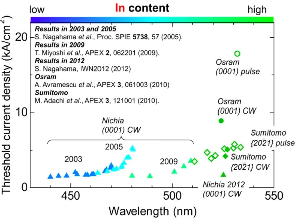
Figure 1.1 Lasing wavelength dependence of threshold current density of III-nitrides LDs.
Threshold current densities with respect to the lasing wavelength are plotted in Fig. 1.1. Until 2008, it seemed very difficult to fabricate LDs beyond 490 nm [4]. However in 2009, Sumitomo electric demonstrated the first pure green LD on the {2021} semipolar GaN substrate [6] and this was followed by a 515 nm LD on the (0001) plane by Nichia Corporation [7]. The former LD on the semipolar plane had a low internal electric field and good homogeneity, and latter was assessed by its excellent homogeneity owing to advanced epitaxial growth. Some companies have released green LDs but their performance needs improvement.
8
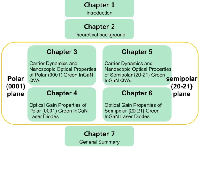
1.3 Construction of this thesis
The objective of this thesis is optical characterization and analysis of green LDs fabricated on (0001) polar plane and {2021} semipolar plane. The contents of the thesis are illustrated in the flow-chart of Fig. 1.2.
Chapter 2 provides the theoretical background on the optical gain and factors that can influence it.
Then, Chapter 3 discusses carrier dynamics and nanoscopic optical properties of polar (0001) green InGaN QWs. The experimental procedure and analysis of the inhomogeneous broadenings are discussed in detail.
Chapter 4 discusses optical gain properties of polar (0001) green InGaN LDs.
Chapter 5 discusses the carrier dynamics and nanoscopic optical properties of semipolar }
1 2 20
{ green InGaN QWs. Then Chapter 6 presents experimental results on the green LDs fabricated on the {2021} semipolar plane.
9
10
References
1) S. Nakamura, M. Senoh, and T. Mukai, Appl. Phys. Lett. 62, 2390 (1993).
2) S. Nakamura, S. Pearton, and G. Fasol, The Blue Laser Diode, 2nd ed. (Springer-Verlag, Heidelberg, 2000).
3) S. Nakamura, M. S. Nagahama, N. Iwasa, T. Yamada, T. Matsushita, H. Kiyoku and Y. Sugimoto, Jpn. J. Appl. Phys. 35, L74 (1996).
4) S. Nagahama, Y. Sugimoto, T. Kozaki, and T. Mukai, Proceeding of SPIE, 5738, 57 (2005).
5) OSRAM 510nm 515nm 520nm 532nm 30mw Green Laser Diode LD PL515 TO38 3.8mm New, http://www.ebay.com/itm/OSRAM-510nm-515nm-520nm-532nm-30mw-Green-Laser-Diode-LD-PL515-TO38-3-8mm-New-/111073607448.
6) Y. Enya, Y. Yoshizumi, T. Kyono, K. Akita, M. Ueno, M. Adachi, T. Sumitomo, S. Tokuyama, T. Ikegami, K. Katayama, and T. Nakamura, Appl. Phys. Exp. 2, 082101 (2009).
7) T. Miyoshi, S. Masui, T. Okada, T. Yanamoto, T. Kozaki, S. Nagahama, and T. Mukai,
Appl. Phys. Exp. 2, 062201 (2009).
8) A. Avramescu, T. Lermer, J. Muller, C. Eichler, G. Bruederl, M. Sabathil, S. Lutgen, and U. Strauss, Appl. Phys. Exp. 3, 061003 (2010).
9) M. Adachi, Y. Yoshizumi, Y. Enya, T. Kyono, T. Sumitomo, S. Tokuyama, S. Takagi, K. Sumiyoshi, N. Saga, T. Ikegami, M. Ueno, K. Katayama, and T. Nakamura, Appl. Phys.
Exp. 3, 12001 (2010).
10) T. Takeuchi, H. Amano, and I. Akasaki, Jpn. J. Appl. Phys. 39, 413 (2000). 11) S. H. Park and S L. Chuang, Phys. Rev. B 59, 4725 (1999).
11
12) T. Melo, Y-L Hu, C. Weisbuch, M. C. Schmidt, A. David, B. Ellis, C. Poblenz, Y. –D. Lin, M. R. Krames, and J. W. Raring, Semicond. Sci. Technol. 27, 024015 (2012).
13) D. Sizov, R. Bhat, K. Song, D. Allen, B. Paddock, S. Coleman, L. C. Hughes, and C. Zah, Appl. Phys. Exp. 4, 102103 (2011).
14) K. Okamoto, J. Kashiwagi, T. Tanaka, and M. Kubota, Appl. Phys. Lett. 94, 071105 (2009).
15) I. Ho and G. B. Stringfellow, Appl. Phys. Lett. 69, 2701 (1996).
16) A. Avramescu, T. Lermer, J. Muller, S. Tautz, D. Queren, S. Lutgen, and U. Strauss,
13
Chapter 2.
Theoretical Background and Literature Survey
2.1 Potential modulations
As discussed in Chapter 1, light emitters based on III-nitrides suffer from large internal electric fields and inhomogeneous broadening caused by tail states. Before discussing properties of the InGaN layer, it is important to define and understand potential modulations that influence the InGaN QW. Two phenomena are the major contributors and are referred to as potential modulations in this study, as shown in Fig. 2.1. The first contribution is from exciton/carrier localization in the InGaN layers due to fluctuation of the In composition in the lateral direction. This fluctuation is caused by the immiscibility between GaN and InN. Sometimes this in-plane modulation makes the device efficient by exciton localization in low carrier density region, but it also deteriorates the device performance such as spectral broadening. The other contribution is from the internal electric fields caused by piezoelectric polarization along the growth direction, as illustrated in Fig. 2.1.
14
2.1.1 Potential fluctuation: in-plane modulation
Numerous efforts have been made to understand the potential fluctuations in III-nitrides. Inhomogeneous broadening of InGaN caused by carrier/exciton localization is of great interest. This potential fluctuation occurs naturally due to the non-uniform formation of InGaN layer, which causes carriers to preferentially flow towards lower potential energy regions called localization centers. Spatial localization of carriers restrains the mobility in the in-plane direction of the QW. This, in turn, either interferes with the capturing of the carriers at non-radiative recombination centers [1, 2], or results in the reduction of recombination probability by decrease of effective area [3]. The former effect increases the internal quantum efficiency in low carrier density regions, as it is mainly governed by localized carriers. This explains the high internal quantum efficiency (IQE) achieved even in III-nitrides systems that have a threading dislocation density of greater than 108/cm2.
To express the potential fluctuation mathematically, we assume that it follows a Gaussian distribution with standard deviation σ,
(2.1)
where Eg0 is the average bandgap.
To study the optical properties of the system, we need to calculate the density of states (DOS, ρ). Since the potential fluctuation is given by Eq. (2.1), we can determine modified DOS ρ’ by convoluting the DOS ρ with the Gaussian distribution G. The DOS ρ is a step function for a QW. This gives
(2.2)
,
2
)
(
exp
2
1
)
,
(
2 2 0
E
E
gE
G
),
,'
(
)
'
(
'
)
(
'
E
dE
E
G
E
E
15
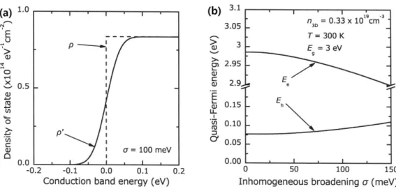
Figure 2.2(a) displays plots of the functions ρ and inhomogeneously broadened DOS ρ’ with respect to the conduction band energy. Furthermore, the energy distribution of the carriers f(E), is a function of Ee and Eh, and follows a Fermi-Dirac distribution governed by
the carrier temperature T and Fermi energy. The energy distributions for the electrons and holes are given by the following equations:
(2.3)
(2.4)
where β = (kBT)-1, kB is the Boltzmann constant, Ee is the conduction band energy, and Eh is
the valence band energy. Figure 2.2(b) shows the change in the quasi-Fermi levels with respect to the inhomogeneous broadening.
,
)])
(
exp[
1
(
)
(
1
,
)])
(
exp[
1
(
)
(
)
(
1 1
h h v e e cE
f
f
E
f
f
Figure 2.2 (a) DOS with inhomogeneously broadened tail states and (b) variation of quasi-Fermi levels due to inhomogeneous broadening. (reprinted from Ref. [10].)
16
2.1.2 Internal electric field: out-of plane modulation
The other important physics in III-nitrides is piezoelectric polarization. Polarized charges are created in the strained hetero-interfacial area by piezoelectric polarization since nitrides are strongly piezoelectric crystals. There is also some contribution from spontaneous polarization. Therefore, quantum confinement Stark effect (QCSE) typically occurs along the growth direction in hetero-QW structures [4]. In light emitters based on interband transition, QCSE is an undesirable effect. In the following subsections, spontaneous and piezoelectric polarizations are discussed in detail.
2.1.2.1 Spontaneous polarization, P
spSpontaneous polarization indicates natural polarization, which is not induced by any strain. We assume a simple model for spontaneous polarization, as shown in Fig. 2.3(a). The dipole moments are compensated by each other in this configuration where the N atoms are positioned at each edge of a regular tetrahedron surrounding the Ga atom. Therefore, in this configuration no piezoelectric field is generated. However, in reality, the atom position is displaced from the ideal tetrahedron due to the iconicity. This displacement breaks the symmetry and causes the spontaneous polarization.
The spontaneous polarization directs along the [0001] direction. Note, spontaneous polarization is not dependent on the nature of the atomic bonding and is only influenced by the atomic configuration.
17
Figure 2.3 (a) Spontaneous and (b) piezoelectric polarizations in crystal.
2.1.2.2 Piezoelectric polarization, P
pzThe internal electric field in the InGaN system is the sum of spontaneous and piezoelectric fields. However, the piezoelectric gives the dominant contribution with increase in In composition. Piezoelectric polarization is strongly related to the strain in the active layer. Most InGaN base devices consist of a hetero-structure. Such hetero-systems are inevitably subject to strain because of the mismatch in lattice parameters between the active and surrounding layers. The dipole moments do not compensate each other when a strain, caused by the lattice mismatch between GaN and InGaN, exists. This leads to piezoelectric polarization, as shown in Fig. 2.3(b). Electrons and holes are separated in space by the electric field induced by the polarization effect, and are likely to move towards the opposite barrier sides. Consequently the overlap integral of the wavefunctions of electrons and holes
18
becomes smaller resulting in a reduction in radiative recombination probability. This phenomenon plays major role in deterioration of IQE of LEDs and LDs.
Strain can be expressed by the degenerated tensor,
. (2.5)
To define the orientation of materials, the orthogonal coordinates are defined and are represented as lower letters. z represents the direction parallel to the growth direction and x, y are orthogonal to each other and lie in the basal plane.
General Hooke’s law relates the piezoelectric polarization Ppz to the strain εij through
piezoelectric tensor eij or dij. The relation between strain εij and piezoelectric polarization Ppz
can be simplified by using the elasticity constants cij with respect to a wurztite structure [4, 5];
(2.6) (2.7) xy zx yz zz yy xx pz e e e e e P
2 2 2 0 0 0 0 0 0 0 0 0 0 0 0 0 33 31 31 15 15 . 2 2 2 0 0 0 0 0 0 0 0 0 0 0 0 0 0 0 0 0 0 0 0 0 0 0 0 0 0 0 0 0 0 0 0 0 0 0 0 0 66 44 44 33 13 13 13 12 12 13 12 11 33 31 31 15 15 xy zx yz zz yy xx c c c c c c c c c c c c d d d d d
.
)
2
2
2
(
T xy zx yz zz yy xx ij
19
Consequently piezoelectric polarization for each orientation is given by
(2.8)
(2.9)
(2.10)
Here, we consider to be the component along the growth orientation. The internal electric fields Ewell Ebar
int
int , are given by summation of
sp pz P
P and .
(2.11)
(2.12)
where the subscript/superscript “bar” indicates barrier, and i (i = well or bar) is the dielectric
constant. The internal electric fields in single QW (SQW) are
(2.13) (2.14) (2.15)
Particularly when the growth is on the (0001) plane, stress on the (0001) polar plane is 0, and the strain becomes
(2.16) . 33 33 13 31 13 33 12 11 31 44 15 44 15 ) 2 ( ) }( ) ( { ) 0 when, 0 ( , 2 , 2 zz yy xx pz z yz pz y yz pz y xz pz x c d c d c d c c d P P c d P c d P
, , ) / ( int int , , , , int well bar well bar bar well bar well well pz z well sp z bar pz z bar sp z well E L L E L L P P P P E
. 0 , SQW in 0 , int , , , int , bar bar well well pz z well sp z bar sp z well bar pz z E p P E E P L
. 2 2 33 12 33 13 yy xx zz c c c c
20 Thus, there is just one independent variable.
As derived above, the piezoelectric polarization increases linearly with strain. This implies that as the In composition in InGaN well layer increases, the polarization also increases. Consequently, an increased piezoelectric polarization induces higher internal electric field. Note, in such system, the electric field contribution from pn built-in or spontaneous polarization is relatively smaller than the contribution from piezoelectric polarization.
2.1.2.3 Crystal angle dependence of internal electric field
In the last section, we derived a mathematical expression for piezoelectric polarization and explained the relationship with the spontaneous polarization and built-in electric field, for the polar (0001) plane. In this section, we will explore these relations for other crystal planes. For this, it is necessary to derive the conversion base matrix in hexagonal system. The crystal angle between a random (hkil) plane and (0001) plane, θ, is given by
(2.17)
where, a and c are lattice parameters of wurtzite crystal. A representative crystal orientation is shown in Fig. 2.4.
x and y correspond to the base axis in the (0001) plane, and z is the axis perpendicular to
the (0001) plane. We set x and y as 1120 and 1010, respectively. To derive a general relation for any tilted angle, the following rotation matrix is used to transform the coordinates. , 4 3 4 3 4 3 arccos 2 1 2 2 2 2 2 2 2 2 c a hk k h c a l c a
21
(2.18)
(2.19)
Here the letters having upper primex', 'y , and 'z are the new coordinates obtained by applying the rotation matrix U to the original coordinates x, y, and z.
Figure 2.4 Representative crystal planes and axes.
.
'
'
'
,
cos
sin
sin
cos
sin
0
cos
sin
sin
sin
cos
cos
cos
z
y
x
U
z
y
x
U
22
The expression for piezoelectric polarization in the new coordinate x’, y’, and z’ can be generalized by multiplying Eqs. (2.6) or (2.7) with the rotation matrix U. is the angle between y and y’, but we take the y axis as the rotational axis. Therefore, y always coincides with y’, and therefore, is zero, which provides following expressions:
(2.20) (2.21) (2.22)
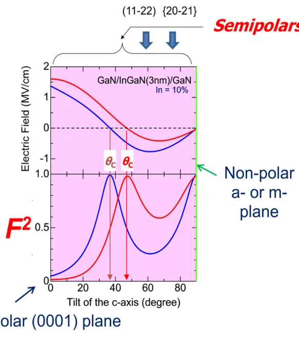
The tilted crystal angle dependence of the piezoelectric polarization and internal electric field are shown in Fig. 2.5 for an In composition of 30 %.
.
cos
sin
,
sin
,
sin
cos
' ' '
pz z pz x pz z y pz x pz y pz z pz x pz xP
P
P
P
P
P
P
P
P
0 30 60 90 -0.01 0.00 0.01 0.02 0.03 (a) 0 30 60 90 -4 -3 -2 -1 0 1Crystal angle (deg.)
In te rn al fi el d ( M V/ cm) Eint, z'well Eint, x'well
Crystal angle (deg.)
Pie zoe le ct ric polariz atio n (C /m 2 ) P pz z' P pz cos z P pz sin x
Figure 2.5 (a) Piezoelectric polarization in In0.3Ga0.7N/GaN QW, and (b) internal
electric field with respect to tilted crystal angle. (reprinted from ref. [10].)
0 30 60 90 -5 -4 -3 -2 -1 0 1 Al0.7Ga0.3N/AlN
Crystal angle (deg.)
In te rn al f ie ld (MV /cm) In0.3Ga0.7N/GaN (b) (a) (b)
23
Figure 2.6 Tilt crystal angle dependence of internal electric field and square of overlap integral. In composition is 10 % in InGaN well layer.
24
It is interesting to note that there are two angles at which the piezoelectric fields and internal electric fields are 0. One is 90 of non-polar plane and the other is a certain angle (dependent on material parameters used for the calculation) known as the semipolar plane. This encourages us to research semipolar-plane based devices. Another important parameter for light emitters is the square of the overlap integral between hole and electron wavefunctions. This is directly related to the recombination probability. Figure 2.6 shows tilted angle dependence of the electric field and the square of the overlap integral in InGaN QW with 10% In composition.
2.2 Optical gain
2.2.1 Formula of gain contributed by material parameters
The optical gain of a laser in a homogeneous system can be expressed as
(2.23)
(2.24)
where | |, | ∙ |, DOS(k)F(k), and L(k) are transition dipole moment, overlap integral between electron and hole wavefunctions, product of density of states and distribution which is related to the effective mass, and homogeneous line width function, respectively. Homogeneous broadening is treated as a constant (25 meV), which is included as a hyperbolic secant function (sech). In this section, those parameters are investigated for the contribution on gain formation. To calculate absolute value of gain the constant C is defined as
)
(
)
(
)
(
)
(
)
(
2 2 0 0 homog
dk
M
k
DOS
k
F
k
L
k
G
cv
c
v ), ) ( ' ( ) 1 ( ) ( 2 0 2
C
dkMcv k fc fv L k h 25
(2.25)
where, , c0, e0, and m0 is degenerated Plank constant, light velocity in vacuum, electronic
charge, and mass. Lw is the thickness of QWs, and nr is the refractive index. By the
modulation of In content in the QWs, peak energy of the gain spectrum can vary dramatically. When inhomogeneous broadening is accounted for by the Gaussian distribution, the mean energy of the distribution is re-defined as average bandgap, Eg0. The gain for an
inhomogeneous system (Ginh) is expressed by convoluting the gain for a homogeneous
system with the Gaussian distribution G.
(2.26)
The mode gain (g), which determines the laser characteristics, has the following relation with
Ginh:
(2.27)
where, αi is internal loss, and Γ is the light confinement factor. Γ is determined by the
analysis of light propagation, based on the LD structure. The internal loss of the diodes can be evaluated from the gain spectra obtained experimentally.
2.2.2 In-plane potential modulation
Since the infancy of nitrides research, in-plane potential modulation has been studied extensively as it leads to carrier localization. Early research mainly focused on the internal quantum efficiency, while the optical gain of nitrides laser diodes was not investigated. As
in-,
2
2 0 0 0 2 0
r wm
n
L
c
e
C
1
d
'
G
homo(
'
)
G
(
E
E
'
).
G
inh
),
1
(
inh
G
ig
26
plane potential modulation becomes larger, maximum gain decreases around the peak photon energy. Interestingly, the lower energy side of the gain spectra shows gain generation in low carrier density region as shown in Fig. 2.7. Equation (2.26) mathematically represents the influence of inhomogeneous broadening on optical gain. In this work, the effects of inhomogeneous broadenings known as in-plane potential modulation on the luminescent spectra including EL, PL, and gain have been studied extensively. We note that large In content in the InGaN layer causes several severe problems in green LDs such as spectral broadening, and suppression of gain.
Figure 2.7 Calculation of optical gain spectra with in-plane potential modulation of 25 or 100 meV. (reproduced from Ref. [10].)
27
2.3 Summary
In this chapter, we defined potential modulation and described the components of the optical gain. To explain in-plane modulation we needed to quantify inhomogeneous broadening. Next, the internal electric field also known as out-of plane modulation was described in terms of spontaneous and piezoelectric polarization. Methods to reduce this internal electric field are the topic of intense research. Amongst these methods, the use of semipolar plane of GaN substrate has been developed. The tilt angle dependency is quantified by applying a rotation matrix on the coordinate system.
There are several terms that influence the optical gain such as transition dipole moment of oscillator, product of density of states and distribution, and line width function. We have explained these affect the optical gain.
28
References
1) S. Chichibu, T. Azuhata, and S. Nakamura, Appl. Phys. Lett. 69, 4188 (1996).
2) Y. Narukawa, Y. Kawakami, M. Funato, Sz. Fujita, Sg. Fujita, and S. Nakamura, Appl.
Phys. Lett. 70, 981 (1997).
3) M. Sugawara, Phys. Rev. B 51, 10743 (1995).
4) T. Takeuchi, S. Sota, M. Katsuragawa, M. Komori, H. Takeuchi, H. Amano, and I. Akasaki, Jpn. J. Appl. Phys. 36, L382 (1997).
5) S. H. Park and S. L. Chuang, Phys. Rev. B 59, 4725 (1999).
6) W. W. Chow and S. W. Koch, Semiconductor-Laser Fundamentals (Springer, Berlin, 1999).
7) B. Witzigmann, V. Laino, M. Luisier, U. T. Schwartz, H. Fischer, G. Feicht, W. Wegscheider, C. Rumbolz, A. Lell, and V. Härle, IEEE Phot. Tech. Lett. 18, 1600 (2006). 8) D. Ahn, S. L. Chuang, and Y. C. Chang, J. Appl. Phys. 64, 4056 (1988).
9) S.H. Park, S. L. Chuang, J. Minch, and D. Ahn, Semicond. Sci. Technol. 15, 1 (2000). 10) K. Kojima, Dissertation of Ph. D, Kyoto University (2008)
29
Chapter 3.
Carrier Dynamics and Nanoscopic Optical Properties of
Polar (0001) Green InGaN QWs
3.1 Introduction
Green LDs based on InGaN QWs are an important technological target, since they are expected to have various applications including laser display [1]. There are two major factors that hamper their practical application; the first concerns the crystal qualities of In-rich InGaN, which are necessary for green emission, and the second is polarization-induced internal electric fields. Both these are related to the large lattice mismatch between InN and GaN. A key factor in circumventing these issues is the crystallographic orientation along which the device structures are fabricated. Semipolar planes such as (1122) [2] and {2021} [3] show a promising reduction in polarization effects [4, 5]. Furthermore, the optical anisotropy due to their low crystal symmetry may lower the threshold current density (Jth) [6].
Note, that the room temperature (RT) CW operation of pure-green LDs has been realized by InGaN QWs on {2021} GaN substrates [7, 8]. On the other hand, effort has been dedicated to improve the quality of the epilayers on the conventional polar (0001) planes, for realizing green LDs [9, 10]. Recently, impressive progress has been reported for (0001) LDs emitting at 525 nm; a Jth of 1.68 kA/cm2, an output power of 1.01 W, and a wall plug efficiency of
14.1 % [11]. Although the semipolar planes seem better suited for green LDs in terms of physics, the conventional polar (0001) plane has vast amounts of accumulated technological resources. Therefore, it is still an open question as to which plane will be commercially feasible.
Optical characterization is indispensable to the recent remarkable progress in InGaN-based LDs. In literature, the gain properties of the (0001) LDs emitting in the near ultra-violet to green spectral range [12-15] and green {2021} LDs [16] have been reported. These
30
previous studies indicate that as the In composition is increased to obtain a longer wavelength range, potential fluctuations become pronounced and cause gain suppression. In this study, we investigate the optical properties of state-of-the-art green LDs fabricated on the (0001) GaN substrates with particular focus on potential fluctuations.
3.2. Experiments
The laser structures with and without doping were grown by metalorganic vapor phase epitaxy on the (0001) GaN substrates. (Except for doping, the structures are identical.) The former (doped) was processed into 800 2 μm2 ridge waveguide LDs, whereas the latter was
used to assess fundamental optical properties. Optical characterization for the LDs, including gain properties, is discussed in Chapter 4.
31
3.2.1 Macroscopic optical measurement system
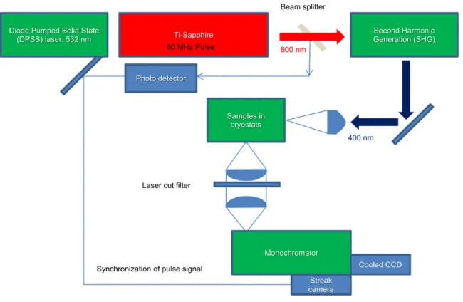
The excitation source for optical assessment was a frequency doubled Ti-sapphire laser. The Ti-sapphire is excited by an 8 W diode pumped solid state laser that continuously emits 532 nm, and it emits 800 nm at a 2 W output power with a frequency of 80 MHz. To excite InGaN layer, 400 nm is achieved by using second harmonic generation (SHG) with nonlinear crystal optics. We measure the temperature dependence of the luminescence, by loading the sample in a cryostats cooled by the closed cycled compression of He gas. The luminescence is detected by proper convex achromatic lenses to direct the light into a monochromator where a grating disperses the light, and the signal is detected by a charge coupled detector (CCD). For time resolved PL systems, the excitation source is nearly the same, but the luminescence is detected by proper units such as a streak camera, time co-related single photon detector, or EM-photon multiplier tube (PMT). Figure 3.1 illustrates a pico-second pulse width laser system in which the sample temperature is adjusted by closed cycled cryostats.
3.2.2 Nanoscopic optical measurement system
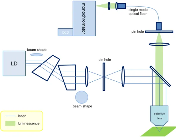
To visualize optical characteristic in the range of a few micrometer, high spatial resolution measurements are necessary. These measurements are restricted by the diffraction limit when using conventional microscopy. The Rayleigh criterion provides a definition of spatial resolution. According to this criterion, we can resolve the spectrum when given a sufficiently small excitation beam size. The spatial resolution is given by
(3.1)
where N.A. is the numerical aperture of objective lens. One of representative ways to resolve the luminescence spatially is confocal micro(nano-)scopic PL measurements. Our set-up at Kyoto University provides about 360 nm spatial resolution when the excitation source
,
N.A.
of
number
61
.
0
x
32
wavelength is 400 nm. This 360 nm resolution is sufficient to assess the local homogeneity distribution of InGaN materials in the green spectral region. The schematic set-up of our confocal microscope PL system is shown in Fig. 3.2. The system is installed on an anti-vibration optical table and in a constant temperature booth to avoid external influences.
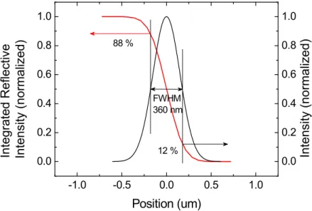
Our set-up uses a 400 nm laser diode as excitation source and an objective lens with a numerical aperture of 0.95. Therefore, theoretically we should obtain ~260 nm resolution from output beam. However, there are several interfering factors such as divergence, and symmetry of the laser beam, which hinder the realization of the theoretical value. The best spatial resolution we obtained was 360 nm, as evaluated by the knife-edge method using atomically cleaved semiconductor substrates. Figure 3.3 shows a schematic of the knife edge method to evaluate spatial resolution.
Figure 3.2 Schematic diagram of confocal micro(nano-)scope PL mapping measurement system.
33
If we assume that the intensity profile of the laser follows a Gaussian distribution, the real position of the full width at half maximum of the intensity corresponds to the spatial resolution of the measurement system. This assumption is illustrated in Fig. 3.4.
-1.0 -0.5 0.0 0.5 1.0 0.0 0.2 0.4 0.6 0.8 1.0 0.0 0.2 0.4 0.6 0.8 1.0 Intensity (normalized) Integrate d Reflec tive Intens ity (normal ized) Position (um) 88 % 12 % FWHM 360 nm
Figure 3.3 Schematic illustration of knife-edge method.
34
3.3. Fundamental optical properties
3.3.1 Inhomogeneous broadening
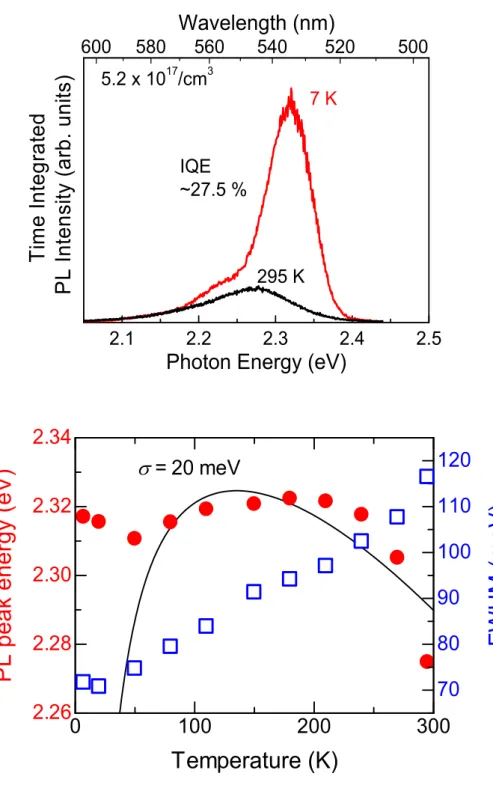
Figure 3.5 indicates the results of photoluminescence for the undoped laser structures. The IQE evaluated from the PL intensity ratio between 7 and 295 K is 27.5 %. As quantified in Fig. 3.5(b), the full width at half maximum (FWHM) is as narrow as 70 meV at low temperatures and 116 meV at RT. Consequently, LO-phonon replicas are well resolved in the PL spectra [Fig. 3.5(a)]. The PL peak energy exhibits a clear S-shape behavior, suggesting carrier/exciton redistribution within potential fluctuations. Assuming a Gaussian distribution of the density of state, the temperature (T) dependence of the PL peak [E(T)] can be fitted with
(3.2)
where Eg(0) is the band gap at 0 K, α and β are Varshni’s fitting parameters, k is the Boltzman
constant, and σ is a standard deviation of the Gaussian distribution [17]. The result of the fit is indicated by solid line in Fig. 3.5(b), providing Eg(0)=2.377 eV and σ ~20 meV. The energy
difference between Eg(0) and the PL emission peak corresponds to the Stokes shift at a low
temperature, which is evaluated to be 60 meV. The σ value of 20 meV corresponds to an FWHM of 50 meV, represents potential fluctuations that excitons can feel during their motion. The difference from the PL FWHM at low temperatures can be attributed to the long-range potential fluctuations, as discussed below. The presence of such short-range and long-range fluctuations has already been discussed [18]. All the quantities (σ =20meV, PL FWHM=70 meV, and a Stokes shift of 60 meV) indicate remarkable suppression of inhomogeneous broadening in the current laser structure, compared with conventional QWs [19]. This is quite advantageous to achieve better differential gain properties [13].
Let us discuss the effects of the inhomogeneous broadening on spatial distribution of PL at RT. A confocal microscope was used for microscopic PL measurements of the undoped green laser structure. In this particular case, the excitation source was an InGaN LD emitting
),
/
/(
)
0
(
)
(
T
E
T
2T
2kT
E
g
35
at 405 nm, and the detection was through a spectrometer. As shown in Fig. 3.6(c), the PL intensity is spatially distributed with island-like structures.
2.1 2.2 2.3 2.4 2.5 5.2 x 10¹⁷/cm3
Wavelength (nm)
295 K 7 KT
im
e In
te
g
ra
te
d
P
L In
te
n
si
ty
(a
rb
. u
n
its)
Photon Energy (eV)
IQE ~27.5 % 600 580 560 540 520 500
0
100
200
300
2.26
2.28
2.30
2.32
2.34
Temperature (K)
PL peak energy (eV)
= 20 meV
70
80
90
100
110
120
FWHM (
m
eV)
Figure 3.5. (a) Time-integrated PL spectra of undoped green laser structures acquired at 7 and 295 K. The photoexcited carrier density is 5 1017/cm3. (b) Temperature
36
Figure 3.6 Fluorescence images of (a) green QW on ELOG GaN template, and (b) green laser structure on GaN substrate. Nanoscopic confocal PL mapping of green laser structure (c) intensity mapping, and (d) wavelength mapping. (e) Relation between intensity and wavelength.
37
However, the distribution is in the range of 78 to 100 % and makes a striking difference from the conventional green QW which showed an intensity fluctuation of more than 90 % [20]. The PL peak energy also fluctuates from 2.320 eV (534.4 nm) to 2.330 eV (532.3 nm), as shown in Fig. 3.6(e). Figures 3.6(c) and 3.6(d) indicate that the long range potential fluctuations suggested in Fig. 3.5 are responsible for an energy variation of 10 meV (2.330-2.320 eV) within the spatial resolution of the confocal microscopy.
The spatial distribution revealed in Fig. 3.6 supports the aforementioned argument that the inhomogeneous broadening is well suppressed in the state-of-the-art green laser structure.
Figure 3.7 Time-integrated PL spectrum and recombination lifetimes (closed circles) at 7 K. The photoexcited initial carrier density is 5 x 10¹⁵/cm3. Weakly localized exciton model (solid line) provides a radiative lifetime of 66 ns.
3.3.2 Exciton/carrier dynamics
To assess exciton/carrier dynamics in the undoped green laser structures, time-resolved PL measurements (TRPL) were performed at 7 K with low carrier density to avoid many body effects, and 5 x 10¹⁵/cm3 is low enough to do so.
2.1
2.2
2.3
2.4
2.5
7 K
5 x 10
15/cm
3Decay Time (ns)
Time I
nt
egrat
ed
PL I
n
tensit
y (arb.
unit
s)
Photon Energy (eV)
0
10
20
30
40
50
60
70
rad: 66 ns
E
me: 2.33 eV
E
0: 32 meV
38
Figure 3.7 shows time-integrated PL spectrum and recombination lifetimes. The estimated lifetimes plotted in Fig. 3.7 are affected solely by radiative recombination processes, particularly at low temperatures such as 7 K. Using a weakly localized exciton model [21], the estimated radiative recombination lifetime is 66 ns (solid line in the Fig. 3.7). It is noteworthy that a conventional 3-nm-thick green QW with an In composition of 25 % exhibits a radiative recombination lifetime of 138 ns [22]. Therefore, the current green laser structure is likely to adopt thinner QWs to avoid the influence from the polarization field.
3.3.3 In composition and well width
From the experimental data presented in section 3.3.1 and 3.3.2, an In composition and a well width in the green laser structure can be deduced. The important parameters are Eg(0) =
2.337 eV and the radiative recombination lifetime of 66 ns. Figure 3.8 indicates the calculated transition energy at 0 K, square of the overlap integral of the electron and hole wavefunctions, and internal electric field as functions of In composition. The longitudinal broken line in the bottom panel of Fig. 3.8 represents the experimentally obtained transition energy, Eg(0). The experimentally determined radiative lifetime in the undoped green laser
structure is 66 ns, whereas that in the conventional green QW (In=25%, well width=3nm) is 138 ns, as commented above. Because the square overlap integral is inversely proportional to the radiative recombination lifetime, that in the undoped green laser structure should be 138/66 times larger, which is designed by the broken line in the middle panel of Fig. 3.8. Our green laser structure must satisfy both the conditions simultaneously. Thus, an In composition of 28+2% and a well width of 2.5+0.27 nm (9+1 monolayers) were derived. The errors were evaluated from the PL line width. Using those quantities, the magnitude of the internal electric field was estimated to be ~2.7 MV/cm. those quantities are indicated by open circles in the Fig. 3.8.
It is noteworthy that the optimization of the epilayer structure for green LDs is directed toward thinner QWs with higher In composition, though the crystal growth becomes difficult due to high In compositions.
39
Figure 3.8 Transition energy at 0 K, square of the overlap integral of electron and hole wavefunctions, and internal electric field as functions of In composition. The well width (Lw)
40
3.4 Summary
It is investigated the optical properties of the state-of-the-art green LD structure fabricated on (0001) GaN substrates, with the particular interest in PL inhomogeneity. The inhomogeneous potential fluctuations were drastically suppressed, compared with conventional QWs. In addition, thinner QWs with higher In compositions were used to improve radiative recombination probability. Those efforts have paid off to lower the threshold current densities in the recent (0001) green LDs.
41
References
1) M. Funato, M. Ueda, Y. Kawakami, Y. Narukawa, T. Kosugi, M. Takahashi, and T. Mukai, Jpn. J. Appl. Phys. 45, L659 (2006).
2) Y. Enya, Y. Yoshizumi, T. Kyono, K. Akita, M. Ueno, M. Adachi, T. Sumitomo, S. Tokuyama, T. Ikegami, K. Katayama, and T. Nakamura, Appl. Phys. Exp. 2, 082101 (2009).
3) T. Takeuchi, H. Amano, and I. Akasaki, Jpn. J. Appl. Phys. 39, 413 (2000). 4) S.-H. Park and S. L. Chuang, Phys. Rev. B 59, 4725 (1999).
5) S.-H. Park, Jpn. J. Appl. Phys. 42, L170 (2003).
6) Y. Yoshizumi, M. Adachi, Y. Enya, T. Kyono, S. Tokuyama, T. Sumitomo, K. Akita, T. Ikegami, M. Ueno, K. Katayama, and T. Nakamura, Appl. Phys. Exp. 2, 092101 (2009). 7) S. Takagi, Y. Enya, T. Kyno, M. Adachi, Y. Yoshizumi, T. Sumitomo, Y. Yamanaka, T.
Kumano, S. Tokuyama, K. Sumiyoshi, N. Saga, M. Ueno, K. Katayama, T. Ikegami, T. Nakamura, K. Yanashima, H. Nakajima, K. Tasai, K. Naganuma, N. Fuutagawa, Y. Takiguchi, T. Hamaguchi, and M. Ikeda, Appl. Phys. Exp. 5, 082102 (2012).
8) T. Miyoshi, S. Masui, T. Okada, T. Yanamoto, T. Kozaki, S. Nagahama, and T. Mukai,
Appl. Phys. Exp. 2, 062201 (2009).
9) A. Avramescu, T. Lermer, J. Muller, C. Eichler, G. Bruederl, M. Sabathil, S. Lutgen, and U. Strauss, Appl. Phys. Exp. 3, 061003 (2010).
10) S. Nagahama, Intern. Workshop on Nitride Semiconductor 2012, PL4, Sapporo, Japan (2012).
11) K. Kojima, M. Funato, Y. Kawakami, S. Nagahama, T. Mukai, H. Braun, and U. T. Schwarz, Appl. Phys. Lett. 89, 241127 (2006).
42
12) K. Kojima, M. Funato, Y. Kawakami, S. Nagahama, and T. Mukai, Opt. Exp. 15, 7330 (2007).
13) W. G. Scheibenzuber, U. T. Schwarz, T. Lermer, S. Lutgen, and U. Strauss, Appl, Phys.
Lett. 97, 021102 (2010).
14) T. Lermer, A. Gomez-Iglesias, M. Sabathil, J. Muller, S. Lutgen, U. Strauss, B. Pasenow, J. Hader, J. V. Moloney, S. W. Koch, W. Scheibenzuber, and U. T. Schwarz, Appl. Phys.
Lett. 98, 021115 (2011).
15) Y. S. Kim, A. Kaneta, M. Funato, Y. Kawakami, T. Kyono, M. Ueno, and T. Nakamura.
Appl. Phys. Exp. 4, 052103 (2011).
16) P. G. Eliseev, P. Perlin, J. Lee, and M. Osinski, Appl. Phys. Lett. 71, 569 (1997).
17) K. Kazlauskas, G. Tamulaitis, P. Pobedinskas, A. Zukauskas, M. Springs, C.-F. Huang, Y.-C. Cheng, and C. C. Yang, Phys. Rev. B 71, 085306 (2005).
18) K. P. O’Donnell, R. W. Martin, and P. G. Middleton, Phys. Rev. Lett. 82, 237 (1999). 19) A. Kaneta, M. Funato, and Y. Kawakami, Phys. Rev. B 78, 125317 (2008).
20) C. Gourdon and P. Lavallard, Phys. Stat. Sol. B 153, 641 (1989).
21) Y. Kawakami, A. Kaneta, and M. Funato, Mater. Sci. Forum, 590, 249 (2008). 22) B. W. Hakki and T. L. Paoli, J. Appl. Phys. 44, 4113 (1973).
23) E. Kioupakis, P. Rinke, and C. G. Van de Walle, Appl. Phys. Exp. 3, 082101 (2010). 24) K, Okamoto, T. Tanaka. M. Kubota, and H. Ohta, Jpn. J. Appl. Phys. 46, L820 (2007).
43
Chapter 4.
Optical Gain Properties of
Polar (0001) Green InGaN Laser Diodes
In the previous chapter we discussed the fundamental optical properties of a green laser structured sample fabricated on the (0001) GaN substrate. We understood that inhomogeneous broadening and piezoelectric polarization induced internal electric field play significant roles in high In concentration green LDs. Using EL, we can evaluate the optical mode gain by analyzing the intensity ratio between the maximum and minimum values of each longitudinal mode. Optical mode gain properties of LDs from the violet to cyan spectral region were thoroughly investigated [1]. It is noteworthy that gain suppression becomes severe as In composition in the InGaN well layers increases. Inhomogeneous broadening as appears to be the major reason for the suppression. Similar to LEDs, current injection is also an important issue for green LDs, and leads to efficiency droop. As for light confinement, the difference in the refractive indices of the InGaN guiding and AlGaN cladding layers becomes smaller as the wavelength increases. Therefore, the confinement factor of green laser diodes is smaller than that of shorter wavelength laser diodes.
4.1. Optical mode gain
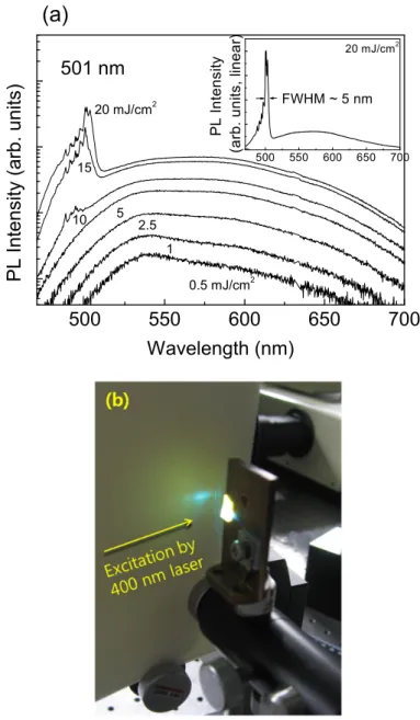
4.1.1 Stimulated emission by optical pumping
Optical pumping was performed by a nano-second pulsed laser of YAG. The sample structure is identical to a laser diode device without doping and lacks mirror facets for the cavity. The excitation energy of optical pumping in the range of 0.5 to 20 mJ/cm2 was
44
examined. As seen in Fig. 4.1(a), sharp stimulated emission is observed for over 10 mJ/cm2. PL is collected by the 50 cm focal length monochromator and then dispersed by 150 gr/mm. Even though the sample does not have any cavity mirrors TE mode is clearly observed as shown in Fig. 4.1(a). Since a sharp lasing-like spectrum is observable even though the emission is stimulated. We infer that the confinement along the vertical growth direction is very strong.
Figure 4.1 (a) Excitation power dependent PL spectra of stimulated emission. (b) Far-field pattern image from the sample.
500 550 600 650 700 500 550 600 650 700 PL In te n sity (a rb. un its, li nea r) FWHM ~ 5 nm 20 mJ/cm2 1 2.5 5 10 15 20 mJ/cm2 PL Intensit y (arb. unit s) Wavelength (nm) 501 nm 0.5 mJ/cm2 (a)
45
4.1.2 Spontaneous and stimulated emission spectra
Figure 4. 2 EL spectra of spontaneous (0.023Jth) and stimulated (1.07Jth) emissions for the
(0001) green LD.
Figure 4.2 compares the EL spectra of the green LD operated below and above the threshold current density (Jth) of 2.75 kA/cm2 (note that because a low-resolution
spectrometer was used for these measurements, the longitudinal modes cannot be resolved). The resultant power efficiency is 6.8% with a driving current density, applied voltage, and output power of 7.63 kA/cm2, 6.0 V, and 50 mW, respectively. The peak energy difference between the spectra below and above the threshold (i.e., 0.023Jth and 1.07Jth, respectively) is
86 meV. This energy shift is almost one-third of that for a conventional blue-green LD used in Refs. [12] and [1](data not shown).
2.1 2.2 2.3 2.4 2.5 2.6
Wavelength (nm)
EL Intensity (arb. units)
Photon Energy (eV)
0.023Jth
x1000
1.07J
th0
46
4.1.3. Hakki and Paoli’s scheme
In early 1970s, Hakki and Paoli measured the optical mode gain under current injection condition [2]. They noticed that the absorption coefficient of the materials in the cavity is related to the modulation depth of longitudinal modes by the interference of Fabry-Perot etalon. Emitted light from the side edge of the sample travels inside the cavity, and so the longitudinal modes are modulated by the cavity. The spacing between these modes is related to the cavity length and wavelength. The green LDs that have a cavity of 600 μm long have ~80 pm mode space at 525 nm. To resolve such a narrow space, a high resolution monochromator is necessary. Therefore, the EL was dispersed by a 1 m monochromator with a resolution of 4 pm. This measurement scheme is illustrated in Fig. 4.3.
47
Let us derive the relation for the optical mode gain measurement proposed by Hakki-Paoli. To this end, we define a damping factor α with respect to the power of the light mode [P(ω)]. Therefore, the damping factor for the electric field amplitude becomes α/2, which is the imaginary part of the propagation parameter. The reflectance coefficients at both the mirrors are R1 and R2. Then electric field amplitude is given by
(4.1)
(4.2)
where En, Lcav, θ represent electric field amplitude, length of cavity, and phase of the electric
field, respectively. When light with frequency ω and mode m travels n times, 2m, and
m(2 1) give the condition for maximum and minimum transmission in the Fabry-Perot cavity. Therefore, electric field satisfying the multiple resonance condition can be expressed in terms of the initial electric field E0 as
(4.3)
While electric field satisfying the anti-resonance condition can be expressed as
(4.4)
Then, we can eliminate E0 from both equations and rewrite with respect to α,
(4.5) (4.6)
)
(
}
)
exp{(
)
(
)
(
12 1 2 1
cav n nR
R
j
L
E
E
),
(
)
(
1
x
E
n.
}
)
(
exp{
)
(
1
)
2
(
)
(
2 1 2 1 0 0 max cav n nL
R
R
E
m
x
E
.
}
)
(
exp{
)
(
1
)
)
1
2
((
)
(
2 1 2 1 0 0 min cav n nL
R
R
E
m
x
E
2 1 min max min max1
ln
2
1
1
)
(
/
)
(
1
)
(
/
)
(
ln
1
)
(
R
R
L
E
E
E
E
L
cav
cav
.
1
ln
2
1
1
)
(
/
)
(
1
)
(
/
)
(
ln
1
2 1 min max min max
R
R
L
P
P
P
P
L
cav
cav
48
Therefore, using the equation above, we can obtain the absorption spectrum α(ω) from the measured light intensity or luminescence P(ω). Note, in the equation above, the first left term on the right hand side is an experimentally measured value and consequently, it becomes 0 just below the threshold current density. The second term on the right side is the compensation of mirror loss designed value. We call the first term the internal total loss and α(ω) the mode gain (or loss).
4.1.4. Injection current density dependent mode gain
Figure 4.4 optical mode gains of a green LD in comparison with shorter wavelength LDs on polar (0001) plane
Dependence of the optical mode gain spectra of the green LD on the injection current density is plotted in Fig. 4.4, in comparison with shorter wavelength LDs. In each LD, the gain value saturates on the lower energy side regardless of the injection current density. These values correspond to the internal loss of the LDs. Interestingly, in Fig. 4.4, the internal loss of the green LD shows the lowest value among the LDs in comparison. This indicates that the sources of internal loss are restricted in the green LD. According to a previous calculation [3] internal loss of green LDs is about 16.5 cm-1. The maximum contribution is from Mg dopant,
2.2 2.3 2.4 2.5 2.6 2.7 2.8 2.9 3.0 3.1 3.2 3.3 3.4 -40 -30 -20 -10 0 10560 540 520 500 480 460 440 420 400 380 374LD 404LD 440LD 512LD 0.19~ 2.69 kA/cm2
Photon Energy (eV)
M
ode Gain (cm
-1 )
470LD