Japan Advanced Institute of Science and Technology
JAIST Repository
https://dspace.jaist.ac.jp/Title
Proton Conductivity and Oriented Structure of Nafion Thin Films on the Au-Deposited Surface and MgO Substrate
Author(s) Nagao, Yuki; Enta, Aoi; Suwansoontorn, Athchaya; Ono, Yutaro
Citation ECS Transactions, 88(1): 249-258 Issue Date 2018-12-13
Type Journal Article
Text version author
URL http://hdl.handle.net/10119/16671
Rights
Copyright (C)2018 ECS. Yuki Nagao, Aoi Enta, Athchaya Suwansoontorn and Yutaro Ono, ECS Transactions, 88(1), 2018, pp.249-258. This is the Accepted Manuscript version of an article accepted for publication in ECS Transactions. The Electrochemical Society and IOP Publishing Ltd are not responsible for any errors or omissions in this version of the manuscript or any version derived from it. The Version of Record is available online at
https://doi.org/10.1149/08801.0249ecst. Description
Proton Conductivity and Oriented Structure of Nafion Thin Films on the Au-deposited Surface and MgO Substrate
Yuki Nagao*, Aoi Enta, Athchaya Suwansoontorn, Yutaro Ono
School of Materials Science, Japan Advanced Institute of Science and Technology, 1-1 Asahidai, Nomi, Ishikawa 923-1292, JAPAN
In-plane proton conductivity and interfacial structure of Nafion thin films on the Au-deposited surface and MgO(100) substrate were investigated. Proton conductivity on both Au-deposited and MgO surfaces clearly decreased with decreasing the thickness except the conditions of 80% and 95% relative humidity on the Au-deposited surface. Proton conductivity drop on the MgO substrate was much heavier than that on the Au-deposited surface. Highly oriented structure was observed in both Nafion thin films on the Au-deposited surface and MgO surface by a p-polarized multiple angle incidence resolution spectrometry. While thickness dependent structural change was observed on the Au-deposited surface like the previous reported Nafion thin films on the Pt-deposited surface, thickness dependence of the structural change was not observed markedly on the MgO substrate.
Introduction
Highly proton-conductive polymers have attracted the attention of researchers for use in energy conversion, sensors, catalysts, and other applications. One fundamental approach to create highly proton-conductive polymers is based on phase segregated structures composed of hydrophobic backbones and hydrophilic parts with strong acid groups (1-3). Nafion is the most investigated proton conductive membrane (4-6).
Since Siroma and co-workers reported on the proton conductivity drop with decreasing the thickness of the Nafion thin films (7), confined Nafion thin films are attracting attention of researchers because of different phase segregated structure and proton transport property compared to the commercial Nafion membranes. Karan and co-workers summarized early works for Nafion thin films (8). Kusoglu and Weber reviewed studies of both Nafion thick membranes and thin films reported by the end of 2016 (6). Many researches on the interfacial structure (8-39) and proton transport property (7, 19-21, 32, 33, 37, 40-48) have been dedicated. Nafion thin films can be prepared from a commercially available dispersion using spin casting, drop casting, Langmuir–Blodgett, Langmuir–Schaefer, spray deposition, and self-assembled adsorption on various substrates. One pioneer study for the interfacial structure of the hydrated Nafion thin film examined an alternating water-rich and polymer-rich lamellar structure on the SiO2 substrate using neutron reflectometry (13). On the other hand, a single hydrated layer appeared at metal interfaces such as Pt and Au surfaces (12, 13). Results suggest that the interfacial structure of the Nafion thin films depends on the substrate surface.
In the previous study, our group demonstrated the in-plane proton conductivity drop of Nafion thin films depends on the substrate surfaces. (19, 20, 33). An inkjet process to
prepare three phase boundary was also demonstrated (49). Surface morphology of Nafion ultrathin film prepared by the inkjet process can be changed to the ultra-smooth surface by a solvent annealing method (47). Compared to the commercially available thick Nafion membrane, all Nafion thin films decreases in-plane conductivity. However, degree of suppressed conductivity is different with the substrate surfaces in the thickness range of several hundreds nano from a few nanometers. To the best of our knowledge, there is no report on the thickness dependence of in-plane proton conductivity of Nafion thin films on the Au and MgO(100) surfaces. The report on the interfacial structure on these surfaces has not also been sufficiently discussed. In this study, thickness dependence of proton conductivity and interfacial structure on the Au-deposited and MgO(100) surfaces were investigated.
Experimental
MgO(100) (Furuuchi Chemical Industries Corp., Japan) and Au-deposited Si wafer were used as substrates. The Si wafer was used as received without removing native oxide layer. The substrate size is 15 × 15 × 0.5 mm. Substrate was washed by 2-propanol and cleaned by plasma treatment (Cute-MP; Femto Science, Korea) (50). Au-deposited Si wafer was prepared using radio frequency (RF) magnetron sputtering system (KXS-110; Kenix Co. Ltd.). Deposition was done in 30 s with 15 W at room temperature with an Ar atmosphere. The thickness of the Au-deposited layer was ca. 10–15 nm determined by atomic force microscopy (AFM) (VN-8000; Keyence Co.) equipped with DFM/SS mode cantilever (OP-75041; Keyence Co.). The Au-deposited surface was characterized using
X-ray photoelectron spectroscopy (XPS) (Kratos AXIS-ULTRA DLD; Shimadzu Corp.). Binding energy was calibrated to C 1s electrons (284.5 eV). Nafion (DE521 CS type; Wako Pure Chemical Industries Ltd.) thin films were prepared with different dispersion concentration by spin-coating. Thickness was determined by AFM measurements and white light interferometric microscope (BW-S506; Nikon Corp.). Proton conductivity of the thin film was examined through impedance measurements using a frequency response analyzer and a high-frequency dielectric interface (SI1260 and SI1296; Solartron Anlytical). Relative humidity (RH) and temperature were controlled using a computer-controlled chamber (SH-221; Espec Corp.). For thin film conductivity measurement, two-probe method was applied to obtain in-plane proton conductivity parallel to the thin film. Gold contacts were used as electrodes with a porous gold paste (SILBEST No. 8560; Tokuriki Chemical Research Co. Ltd.). Impedance data were collected for frequencies of 1 Hz and 10 MHz, with an applied alternating potential of 50 mV. Thin-film conductivity (σ) was calculated as,
σ =𝑅𝑅𝑅𝑅𝑅𝑅𝑑𝑑 , (1)
where d signifies the distance between the gold electrodes, R denotes the resistance value obtained from the impedance, l and t respectively stand the contact electrode length and the thickness of the film. p-Polarized multiple angle incidence resolution spectrometry (pMAIRS) technique (51, 52) was used to investigate the molecular orientation of the thin film on the substrates. The p-MAIRS measurements were taken using an Fourier transform infrared (FT-IR) spectrometer (Nicolet 6700; Thermo Fisher Scientific Inc.) equipped with a mercury–cadmium–telluride (MCT) detector and ZnSe polarizer. Single-beam spectra were collected from 38° to 8° in 6° steps between the angle of incidence. The humidity of the sample compartment was less than 5% under room temperature. The p-MAIRS analysis
from the collected spectra was conducted automatically using p-MAIRS analyzer software (Thermo Fisher Scientific Inc.).
Results and Discussion
Nafion thin films on Au-deposited surface
Thickness dependence of the proton conductivity on the SiO2 substrates has been reported in several literature (7, 21, 33, 43). Siroma and co-workers demonstrated depression of proton conductivity in recast Nafion films (7). The high proton conductivity is derived from a phase segregation between hydrophobic backbone and hydrophilic sulfonic acid groups at the side chain (1, 4, 5). Modestino and co-workers reported that degree of phase segregation decreases with decreasing thickness of the Nafion thin films (21). Ono and Nagao show that the proton conductivity decreases with decreasing the thickness of Nafion thin films on the thin Pt-deposited surface (33). However, the proton transport on the Au-deposited surface has not been sufficiently discussed. For the in-plane
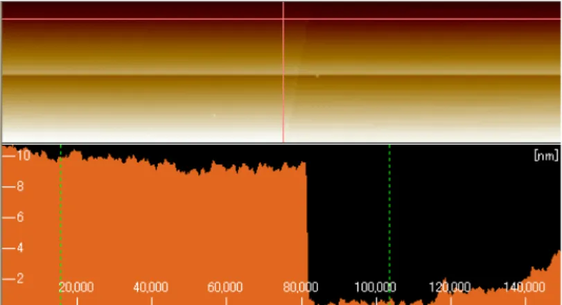
proton conductivity measurements on the deposited surface, thickness of the Au-deposited surface should be thin because of suppressing the electronic conductivity by the Au layer (33). Fig. 1 shows the AFM images of the top and cross section views for the Au-deposited surface on SiO2 substrate. Thickness of Au layer was estimated as 10 nm thick. The resistance of the Au layer was higher than that of the Nafion thin films in the all RH ranges. The Si 2p XPS spectrum suggested that deposited Au formed island structures on the SiO2 surface. Therefore Au deposited layer is not so conductive compared to the Nafion thin film layer.
Figure 1. AFM images of the top view and cross section views for the Au-deposited surface on SiO2 substrate.
Figure 2 shows thickness dependence of proton conductivity of the Nafion thin films on the Au-deposited surface. Proton conductivity of 20, 90, and 200 nm thick films showed 1.5 × 10⁻², 1.7 × 10⁻², and 1.6 × 10⁻² S cm-1 at the 95% RH, respectively. Compared to the thick Nafion membrane, the proton conductivity of Nafion thin films was lower in the thickness range of 20 – 200 nm. In the previous report used by SiO2 and Pt-deposited surfaces, proton conductivity decreased with decreasing thickness (33). In the case of Au-deposited surface, proton conductivity of Nafion thin films showed almost the same value at the 80% and 95% RH. In the lower RH condition, proton conductivity dropped with decreasing the thickness. Compared to the Nafion thin films on the SiO2 substrates, the decrease of the proton conductivity on the Pt- and Au-deposited metal surfaces was
suppressed in the thinner region. Shim and co-workers reported that the water uptake of Nafion thin films with ca. 80 nm thick on SiO2, Pt-deposited, and Au-deposited surfaces exhibit almost similar value in the RH range of 0 – 80% (46). Kusoglu and co-workers suggest the substrate/film interactions influence the structural order (28). Therefore we speculated that the difference of the proton conductivity between the metal and Si wafer surfaces might be derived from the different thin film nano-structures.
-6 -5 -4 -3 -2 -1 0 50 100 150 200 250 40% RH 60% RH 80% RH 95% RH Lo g ( σ / S c m -1 ) Thickness / nm 298K
Figure 2. Thickness dependence of the proton conductivity for the Nafion thin films on the Au-deposited surface at various RH conditions.
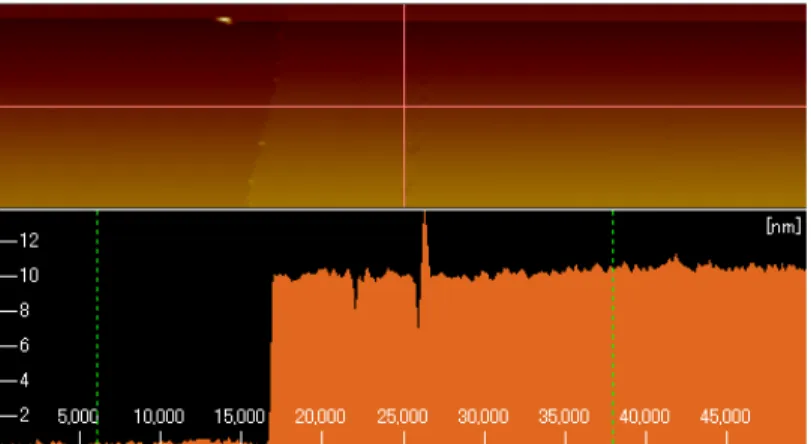
pMAIRS requires transparent substrates (51, 52). To the best of our knowledge, pMAIRS study has not been established using deposited surfaces. Therefore Au-deposition on the Si wafer was optimized. Thickness of Au-deposited surfaces should be thin as possible to apply pMAIRS (33). Fig. 3 shows the AFM images of the top and cross section views for the Au-deposited surface on Si wafer. Thickness of Au was estimated as 10 nm thick. This transmittance of the IR single beam was 95% compared to the non-deposited Si wafer.
Figure 3. AFM images of the top view and cross section views for the Au-deposited surface on Si wafer.
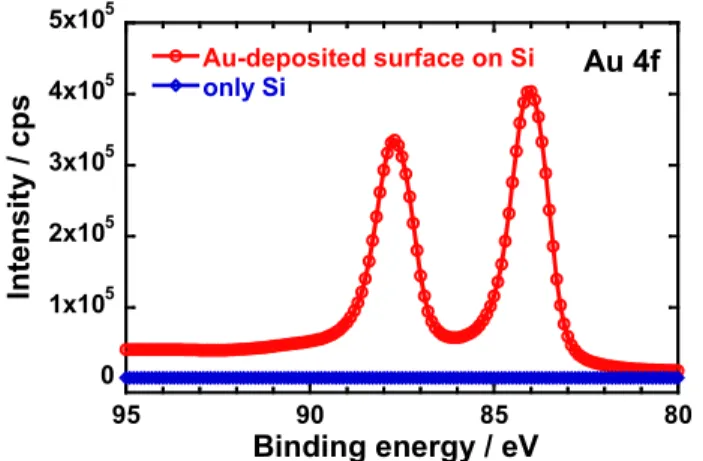
Figure 4 shows Au 4f XPS spectrum for the Au-deposited surface on the Si wafer. Binding energies of Au 4f7/2,4f5/2 electrons at 84.0 eV and 87.7 eV, respectively, suggest
Au0. Since signal in the Si 2p XPS spectrum decreased but was still observed after the Au-deposition, Au was deposited as island structures on the Si wafer.
0 1x10⁵ 2x10⁵ 3x10⁵ 4x10⁵ 5x10⁵ 80 85 90 95 Au-deposited surface on Si only Si In tensi ty / cp s Binding energy / eV Au 4f
Figure 4. Au 4f XPS spectra of bare Si wafer and Au-deposited surface on Si wafer. Figure 5 shows incident angle dependence of the IR transmission spectra of Nafion thin film on the Au-deposited surface. At the wavenumber around 1250 cm-1, absorption band strongly depends on the incident angle. This result suggests that the thin film on the Au-deposited surface exhibited an oriented structure. The highly oriented Nafion thin film on the Pt-deposited surface has been reported in our previous literature (20).
0 0.02 0.04 0.06 0.08 0.10 1100 1150 1200 1250 1300 1350 1400 38 deg 32 deg 26 deg 20 deg 14 deg 8 deg A bs or ba nc e Wavenumber / cm-1
Figure 5. Incident angle dependence of the IR transmission spectra of the 200 nm thick Nafion film on the Au-deposited surface.
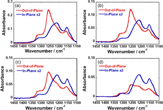
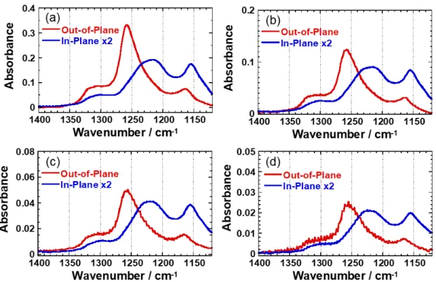
Figure 6 shows pMAIR spectra of Nafion thin films with different thickness on the Au-deposited surface. The bands at 1150, 1210 – 1240, and 1300 cm-1 are assigned to νas (CF2), [νas (CF2) and νas (SO3-)], and ν(C-C) (53). The IP and OP spectra did not show the similar spectral shape. Results suggest that the Nafion thin films on the Au-deposited surface have oriented structure. This orientation has been reported in our previous literature using Si and Pt-deposited surfaces (33). IP spectrum showed the well-known spectrum of the thick Nafion membrane (53). The characteristic band at 1260 cm-1 was observed only in the OP spectrum. This attribution of the absorption band is unsolved yet (54, 55). Some attributions were reported as νas(CF3) + δs(COC) (15), νas(CF2) (35), ν(CF2) (56), νas(CF3) (57), and –SO3- (58, 59) vibration modes. Ozhukil Kollath and co-workers discussed the origin of thickness dependent peak from 1223 to 1259 cm-1 by attenuated total reflection (ATR)-FTIR spectra of Nafion films (60). However, our results showed that the peak
position was thickness independent in the thickness range of 210 – 20 nm. Therefore our observed peak at 1260 cm-1 can be considered as the different origin with the reported thickness dependent peak (35, 60). In our results, each absorbance in the IP and OP spectra decreased with decreasing thickness. The ratio of absorption bands at 1260 cm-1 in the OP spectrum and at 1215 cm-1 in the IP spectrum gradually changed along the thickness change. This large change of the absorption ratio can be observed on the Pt-deposited surface, but not on the Si wafer surface. Results indicate that interfacial structure of Nafion thin films is different between the metal and Si wafer surfaces.
Figure 6. IR pMAIR spectra of Nafion thin films on the Au-deposited surfaces. The
thickness of Nafion thin films is (a)210 nm, (b)150 nm, (c)90 nm, and (d)20 nm thick. Nafion thin films on MgO(100) surface
In the previous section, the decrease of the proton conductivity on the Au-deposited surface was suppressed compared to that on the SiO2 substrates. In our previous study, proton conductivity of Nafion thin films on the MgO(100) substrate strongly decreased compared to that of the commercial thick Nafion membranes (19). To investigate the thickness dependence of in-plane proton conductivity on the MgO(100) substrate, RH-controlled impedance measurements were carried out. Fig. 7 shows thickness dependence of proton conductivity for Nafion thin films on the MgO(100) substrates. The proton conductivity was lower than that on the Au-deposited surface. The conductivity on the MgO(100) substrate decreased by one order of magnitude with decreasing the thickness.
Fig. 8 shows pMAIR spectra of Nafion thin films with different thickness on the MgO(100) substrates. In common with the results on the Au-deposited surface, all thin films showed the highly oriented structure on MgO substrates. The difference between the Au-deposited surface and MgO surface can be seen in the absorption ratio of the bands between 1260 cm-1 in the OP spectrum and 1215 cm-1 in the IP spectrum. The ratio was
almost thickness independent in the case of MgO substrates. Both Au-deposited and Pt-deposited surfaces show the similar trend of the thickness dependent absorption ratio. Though the peak assignment at 1260 cm-1 in the OP spectrum is still unsolved, results demonstrate that the interfacial oriented structure on metal-deposited surfaces gradually changes with decreasing the thickness of Nafion thin films.
-8 -7 -6 -5 -4 -3 0 50 100 150 200 250 40% RH 60% RH 80% RH Lo g ( σ / S c m -1 ) Thickness / nm 298K
Figure 7. Thickness dependence of the proton conductivity for the Nafion thin films on the MgO(100) substrate at various RH conditions.
Figure 8. IR pMAIR spectra of Nafion thin films on the MgO(100) substrates. The thickness of Nafion thin films is (a)240 nm, (b)150 nm, (c)30 nm, and (d)15 nm thick.
In this study, results suggest that the metal-deposited surface can suppress the decrease of the in-plane proton conductivity in the thin film forms of Nafion compared to the SiO2 and MgO(100) substrates. The metal-deposited surface also causes the change of the interfacial oriented structure. Some parameters should be discussed to unveil the origin for the surface-selective structural change: surface charge, surface flatness, surface hydrophilicity, conductivity (derived from electrons and holes), etc. Some parameters can be discussed using self-assembled monolayer techniques in future.
Conclusions
Nafion thin films are attracting attention of researchers because of different phase segregated structure and proton transport property compared to the commercial thick Nafion membranes. In the previous study, proton conductivity drop was reported with decreasing thickness of Nafion thin films on SiO2 substrates. In this study, pMAIRS study using the Au-deposited surface was newly established. Then in-plane proton conductivity and interfacial structure of Nafion thin films on the Au-deposited surface and MgO(100) substrate were investigated. Apparent drop of proton conductivity was observed on both Au-deposited and MgO surfaces compared to the commercial Nafion membrane. A larger proton conductivity drop on the MgO substrate was found than that on the Au-deposited surface. For the interfacial structure by pMAIRS study, highly oriented structure was elucidated in both Nafion thin films on the Au-deposited surface and MgO surface. Nafion thin films on the Au-deposited surface exhibited the thickness dependent structural change. This trend can be seen in the case on the Pt-deposited surface. Results indicate that metal-deposited surfaces gradually changes the interfacial structure with decreasing the thickness of Nafion thin films. In the case of MgO substrates, no apparent structural change was observed. We infer that the metal-deposited surfaces suppress the drop of in-plane proton conductivity of the Nafion thin films compared to the SiO2 and MgO(100) surfaces.
Acknowledgments
Y.N. thanks Dr. Vinayaraj Ozhukil Kollath and Prof. Carol Korzeniewski for their time for discussion. This work was partially supported by JSPS KAKENHI Grant Number JP18K05257.
References
1. K. D. Kreuer, J. Membr. Sci., 185, 29 (2001).
2. M. A. Hickner, H. Ghassemi, Y. S. Kim, B. R. Einsla and J. E. McGrath, Chem. Rev.,
104, 4587 (2004).
3. T. J. Peckham, J. Schmeisser, M. Rodgers and S. Holdcroft, J. Mater. Chem., 17,
3255 (2007).
4. W. Y. Hsu and T. D. Gierke, J. Membr. Sci., 13, 307 (1983).
5. K. A. Mauritz and R. B. Moore, Chem. Rev., 104, 4535 (2004).
6. A. Kusoglu and A. Z. Weber, Chem. Rev., 117, 987 (2017).
7. Z. Siroma, R. Kakitsubo, N. Fujiwara, T. Ioroi, S.-i. Yamazaki and K. Yasuda, J. Power Sources, 189, 994 (2009).
8. D. K. Paul, K. Karan, A. Docoslis, J. B. Giorgi and J. Pearce, Macromolecules, 46,
9. K. Kanamura, H. Morikawa and T. Umegaki, J. Electrochem. Soc., 150, A193
(2003).
10. T. A. Hill, D. L. Carroll, R. Czerw, C. W. Martin and D. Perahia, J. Polym. Sci. Pol. Phys., 41, 149 (2003).
11. K. More, R. Borup and K. Reeves, ECS Trans., 3, 717 (2006).
12. V. S. Murthi, J. Dura, S. Satija and C. Majkrzak, ECS Trans., 16, 1471 (2008).
13. J. A. Dura, V. S. Murthi, M. Hartman, S. K. Satija and C. F. Majkrzak, Macromolecules, 42, 4769 (2009).
14. D. L. Wood, J. Chlistunoff, J. Majewski and R. L. Borup, J. Am. Chem. Soc., 131,
18096 (2009).
15. I. Kendrick, D. Kumari, A. Yakaboski, N. Dimakis and E. S. Smotkin, J. Am. Chem. Soc., 132, 17611 (2010).
16. M. Bass, A. Berman, A. Singh, O. Konovalov and V. Freger, J. Phys. Chem. B, 114,
3784 (2010).
17. M. Bass, A. Berman, A. Singh, O. Konovalov and V. Freger, Macromolecules, 44,
2893 (2011).
18. M. A. Modestino, A. Kusoglu, A. Hexemer, A. Z. Weber and R. A. Segalman, Macromolecules, 45, 4681 (2012).
19. Y. Nagao, e-J. Surf. Sci. Nanotechnol., 10, 114 (2012).
20. Y. Nagao, J. Phys. Chem. C, 117, 3294 (2013).
21. M. A. Modestino, D. K. Paul, S. Dishari, S. A. Petrina, F. I. Allen, M. A. Hickner, K. Karan, R. A. Segalman and A. Z. Weber, Macromolecules, 46, 867 (2013).
22. S. Kim, J. A. Dura, K. A. Page, B. W. Rowe, K. G. Yager, H. J. Lee and C. L. Soles, Macromolecules, 46, 5630 (2013).
23. D. Damasceno Borges, A. A. Franco, K. Malek, G. Gebel and S. Mossa, ACS Nano,
7, 6767 (2013).
24. A. Ohira, S. Kuroda, H. F. M. Mohamed and B. Tavernier, Phys. Chem. Chem. Phys., 15, 11494 (2013).
25. H. F. M. Mohamed, S. Kuroda, Y. Kobayashi, N. Oshima, R. Suzuki and A. Ohira, Phys. Chem. Chem. Phys., 15, 1518 (2013).
26. Y. Ogata, D. Kawaguchi, N. L. Yamada and K. Tanaka, ACS Macro Lett., 2, 856
(2013).
27. I. Yagi, K. Inokuma, K. Kimijima and H. Notsu, J. Phys. Chem. C, 118, 26182
(2014).
28. A. Kusoglu, D. Kushner, D. K. Paul, K. Karan, M. A. Hickner and A. Z. Weber, Adv. Funct. Mater., 24, 4763 (2014).
29. S. C. DeCaluwe, P. A. Kienzle, P. Bhargava, A. M. Baker and J. A. Dura, Soft Matter, 10, 5763 (2014).
30. K. A. Page, A. Kusoglu, C. M. Stafford, S. Kim, R. J. Kline and A. Z. Weber, Nano Lett., 14, 2299 (2014).
31. K. A. Page, J. W. Shin, S. A. Eastman, B. W. Rowe, S. Kim, A. Kusoglu, K. G. Yager and G. R. Stafford, ACS Appl. Mater. Inter., 7, 17874 (2015).
32. A. Kusoglu, T. J. Dursch and A. Z. Weber, Adv. Funct. Mater., 26, 4961 (2016).
33. Y. Ono and Y. Nagao, Langmuir, 32, 352 (2016).
34. V. Ozhukil Kollath and K. Karan, Phys. Chem. Chem. Phys., 18, 26144 (2016).
35. T. J. Zimudzi and M. A. Hickner, ACS Macro Lett., 5, 83 (2016).
36. K. Karan, Curr. Opin. Electrochem., 5, 27 (2017).
37. S. C. DeCaluwe, A. M. Baker, P. Bhargava, J. E. Fischer and J. A. Dura, Nano Energy, 46, 91 (2018).
38. M. Tesfaye, A. N. MacDonald, P. J. Dudenas, A. Kusoglu and A. Z. Weber, Electrochem. Commun., 87, 86 (2018).
39. M. Handl, T. Morawietz, D. K. Paul, K. A. Friedrich, K. Karan and R. Hiesgen, ECS Trans., 85, 889 (2018).
40. Z. Siroma, T. Ioroi, N. Fujiwara and K. Yasuda, Electrochem. Commun., 4, 143
(2002).
41. D. K. Paul, A. Fraser and K. Karan, Electrochem. Commun., 13, 774 (2011).
42. K. Karan, ECS Trans., 50, 395 (2013).
43. D. K. Paul and K. Karan, J. Phys. Chem. C, 118, 1828 (2014).
44. D. K. Paul, R. McCreery and K. Karan, J. Electrochem. Soc., 161, F1395 (2014).
45. A. Z. Weber and A. Kusoglu, J. Mater. Chem. A, 2, 17207 (2014).
46. H. K. Shim, D. K. Paul and K. Karan, Macromolecules, 48, 8394 (2015).
47. Y. Guo, Y. Ono and Y. Nagao, Langmuir, 31, 10137 (2015).
48. T. Morawietz, M. Handl, C. Oldani, K. A. Friedrich and R. Hiesgen, ACS Appl. Mater. Inter., 8, 27044 (2016).
49. Z. Wang and Y. Nagao, Electrochim. Acta, 129, 343 (2014).
50. Y. Nagao, e-J. Surf. Sci. Nanotechnol., 10, 229 (2012).
51. T. Hasegawa, Anal. Chem., 79, 4385 (2007).
52. T. Hasegawa, J. Phys. Chem. B, 106, 4112 (2002).
53. A. Gruger, A. Regis, T. Schmatko and P. Colomban, Vib. Spectrosc., 26, 215
(2001).
54. Y. Nagao, Langmuir, 33, 12547 (2017).
55. Y. Nagao, Kobunshi Ronbunshu (In Japanese) Published online. (DOI:10.1295/koron.2018-0012), (2018).
56. E. M. Davis, C. M. Stafford and K. A. Page, ACS Macro Lett., 3, 1029 (2014).
57. J. B. Zeng, D. I. Jean, C. X. Ji and S. Z. Zou, Langmuir, 28, 957 (2012).
58. D. Malevich, V. Zamlynny, S. G. Sun and J. Lipkowski, Z. Phys. Chem., 217, 513
(2003).
59. C. Korzeniewski, D. E. Snow and R. Basnayake, Appl. Spectrosc., 60, 599 (2006).
60. V. Ozhukil Kollath, Y. Liang, F. D. Mayer, X. Ma, C. Korzeniewski and K. Karan, J. Phys. Chem. C, 122, 9578 (2018).