Japan Advanced Institute of Science and Technology
JAIST Repository
https://dspace.jaist.ac.jp/
Title
Fabrication and Characteristics of C_<84>
Fullerene Field-Effect Transistor
Author(s)
Shibata, K; Kubozono, Y; Kanbara, T; Hosokawa, T;
Fujiwara, A; Ito, Y; Shinohara, H
Citation
Applied Physics Letters, 84(14): 2572-2574
Issue Date
2004-04
Type
Journal Article
Text version
publisher
URL
http://hdl.handle.net/10119/3367
Rights
Copyright 2004 American Institute of Physics.
This article may be downloaded for personal use
only. Any other use requires prior permission of
the author and the American Institute of Physics.
The following article appeared in Kana Shibata,
Yoshihiro Kubozono, Takayoshi Kanbara, Tomoko
Hosokawa, Akihiko Fujiwara, Yasuhiro Ito and
Hisanori Shinohara, Applied Physics Letters
84(14), 2572-2574 (2004) and may be found at
http://link.aip.org/link/?apl/84/2572.
Fabrication and characteristics of C
84fullerene field-effect transistors
Kana Shibata and Yoshihiro Kubozonoa)Department of Chemistry, Okayama University, Okayama 700-8530, Japan and CREST, Japan Science and Technology Corporation, Kawaguchi, 322-0012, Japan
Takayoshi Kanbara
Department of Chemistry, Okayama University, Okayama 700-8530, Japan Tomoko Hosokawa
Department of Chemistry, Okayama University, Okayama 700-8530, Japan and CREST, Japan Science and Technology Corporation, Kawaguchi, 322-0012, Japan
Akihiko Fujiwara
Japan Institute of Science and Technology, Ishikawa 923-1292, Japan and CREST, Japan Science and Technology Corporation, Kawaguchi, 322-0012, Japan
Yasuhiro Ito and Hisanori Shinohara
Department of Chemistry, Nagoya University, Nagoya 464-8602, Japan and CREST, Japan Science and Technology Corporation, Kawaguchi, 322-0012, Japan
共Received 25 November 2003; accepted 9 February 2004兲
Fullerene field-effect transistors 共FETs兲 were fabricated with thin films of C84, which showed
n-channel normally-on depletion-type FET characteristics. The C84 FET device exhibited the highest mobility, , of 2.1⫻10⫺3 cm2V⫺1s⫺1 among normally-on fullerene FETs. The carrier transport of this FET device can be interpreted as thermally activated hopping transport. Carrier type (n-channel兲 and transport mechanism 共hopping兲 reflect the electronic properties of the C84 molecule. © 2004 American Institute of Physics. 关DOI: 10.1063/1.1695193兴
A large number of field-effect transistors 共FETs兲 with thin films of organic molecules have been fabricated and their characteristics have been studied for next-generation electronics during the past decade.1,2The field-effect mobili-tiesof organic FETs are lower by four orders of magnitude than those of conventional FETs with inorganic materials. Nevertheless, organic FETs are known to have many advan-tages such as large-area coverage, structural flexibility, and low-temperature and low-cost processing in comparison with inorganic FETs. In 1997 the mobility of a pentacene
p-channel FET reached 1.5 cm2V⫺1s⫺1.3 Subsequently, a
p-channel FET on single crystals of rubrene showed a
mo-bility of 1.0 cm2V⫺1s⫺1.4
The first fullerene FET was fabricated with thin films of C60 by Haddon et al.5 This FET device showed a high mo-bility of 0.08– 0.3 cm2V⫺1s⫺1. The high value of this device implies that C60 FETs can play an important role in future applications such as identification tags, smart cards, and drivers for active-matrix displays based on the integra-tion with organic light-emitting diodes. The mobility values of n-channel organic FETs except for the C60FET are much lower than those of p-channel organic FETs.1,2Furthermore, such high value attracts interest in the physics and chem-istry of C60FETs. The improvement of properties of the C60 FET device has long been examined, and very recently the mobility reached 0.56 cm2V⫺1s⫺1, which is one of the highest mobilities among n-channel organic FETs.6 The
highest of 0.6 cm2V⫺1s⫺1 was reported for
N,N
⬘
-dialkyl-3,4,9,10-perylene tetracalboxylic diimide de-rivative共PTCDI-C8H兲 FET device.7Recently we reported the transport properties of C60 FET.8 Temperature dependence of the mobility suggested a hopping transport as a conduction mechanism for these FETs. Furthermore, a complementary metal–oxide–semi-conductor logic gate circuit was fabricated with C60and pen-tacene FETs,8which leads us to realize various types of logic circuits such as NOR and NAND for computing and memory. The first FETs with metallofullerenes have been realized with Dy@C82 and [email protected],9 These FETs oper-ated as n-channel normally-on device, which is substantially different from enhancement-type FETs with C60 and C70.5,6,8,10 The output characteristics of fullerene FETs, therefore, reflect intrinsic electronic structures of individual fullerene molecules. This letter reports on the fabrication of higher-fullerene FET devices with thin films of C84, and the FET characteristics and their temperature dependence.
Schematic representation of C84 (D2d isomer兲 and a cross-sectional view of the C84FET device are shown in Fig. 1共a兲. Commercially available C84 共99%兲 was used for the fabrication of the thin film. Commercially available SiO2/Si(100) wafers were used as substrates after cleaning with acetone, methanol, and H2SO4/H2O2. The thin film of C84 was formed by a thermal deposition under a vacuum of 10⫺8 Torr. The channel length L and the channel width W of this device were 75 and 4000m, respectively. The charac-teristics of the C84 FET device were measured under 10⫺6 Torr after annealing for 24 h at 120 °C under 10⫺6 Torr.
The drain current ID versus drain–source voltage VDS plots for the C84 FET at 290 K are shown in Fig. 1共b兲. The a兲Electronic mail: [email protected]
APPLIED PHYSICS LETTERS VOLUME 84, NUMBER 14 5 APRIL 2004
2572
0003-6951/2004/84(14)/2572/3/$22.00 © 2004 American Institute of Physics
plots show output characteristics of n-channel normally-on depletion-type FET. Relatively large ID is observed even at zero gate voltage VG. By varying VGfrom⫺130 to 130 V,
IDincreases as VGincreases as shown in Fig. 1共b兲. It can be seen that the channel conductance decreases by applying a negative VG, presumably due to the depletion of carriers in the channel. ID remained constant below VG⫽⫺70 V. This can be explained by assuming the existence of bulk current which cannot be reduced by applying the negative VG. The threshold voltage VT was estimated to be ⫺42 V from the
ID– VGplot at VDS⫽10 V 关Fig. 1共c兲兴. The negative VT sup-ports that the C84 FET is normally-on type. Very recently such a normally-on depletion-type property was observed in La2@C80 FET.9
The field-effect mobility for the C84 FET was estimated to be 1.1⫻10⫺3cm2V⫺1s⫺1 from the ID– VG plot 关Fig. 1共c兲兴. This value is higher by one order of magnitude than those reported for Dy@C82 and La2@C80 FETs.8,9This im-plies that C84 is superior to metallofullerenes such as Dy@C82 and La2@C80 as materials for an active layer in normally-on depletion-type FET. Theincreases
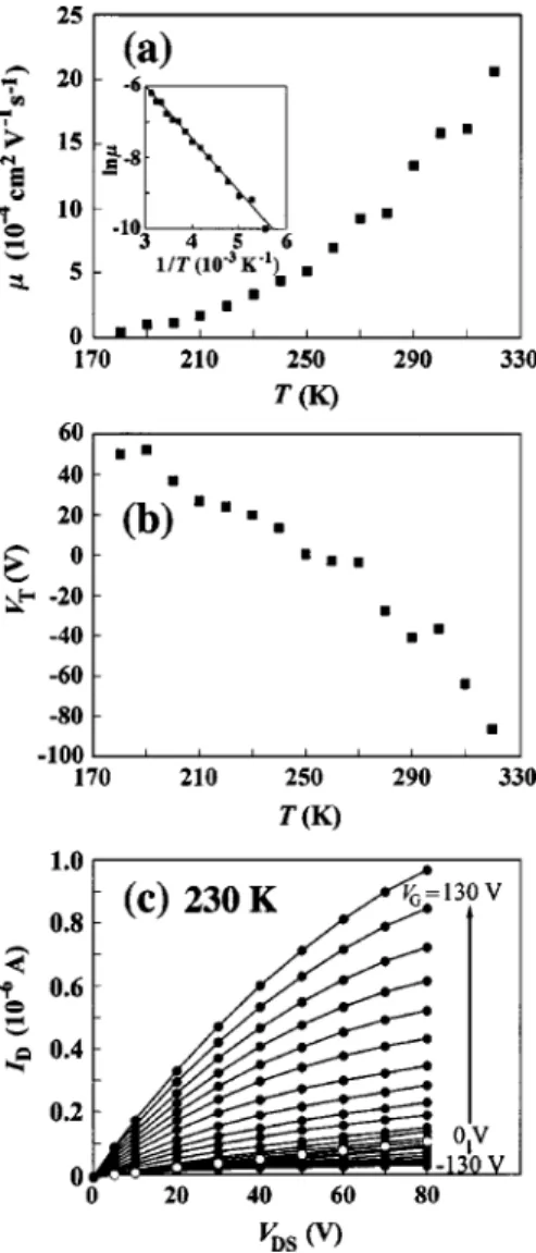
monotoni-cally as temperature increases up to 320 K 关Fig. 2共a兲兴; the mobility reached 2.1⫻10⫺3 cm2V⫺1s⫺1at 320 K. FET be-havior was not clearly observed below 180 K because of very small ID. The activation energy Ea was estimated to be 0.13 eV from the lnversus T⫺1plot shown in the inset of Fig. 2共a兲. These results show that the channel conduction of the C84 FET device follows a thermally activated hopping-transport model (⬃exp⫺Ea/kBT). One of the origins of
highin the C84FET may be attributed to the fact that the channel conduction occurs through a hopping between the delocalized lowest unoccupied molecular orbitals 共LUMOs兲 in C84, which is different from that between the localized
LUMOs dominated by encapsulated metal ions in
metallofullerenes.9
The threshold voltage VT decreases monotonically with increasing temperature up to 320 K 关Fig. 2共b兲兴. Such tem-perature dependence might be caused by an increase in bulk current. Actually the bulk current increased with increasing temperature,11which results in an apparent variation in VT. The VTvalues are positive at temperatures below 250 K, and the FET property apparently changes from the normally-on to a normally-off with decreasing temperature. As an
ex-FIG. 1. 共a兲 Schematic picture of C84(D2d) and cross-sectional view of C84
FET.共b兲 ID– VDSplots of C84FET at 290 K. Closed and open circles refer
to the points measured at VG⫽0 V and VG⫽0 V, respectively. 共c兲 ID– VG
plot at VDS⫽10 V. Solid line is the line fitted with equation ID
⫽(WC0/L) (VG– VT)VDS, where C0refers to capacitance of SiO2; C0 ⫽8.22⫻10⫺9F cm⫺2.
FIG. 2.共a兲– T plot of C84FET and ln-(1/T) plot in the inset. Solid line is the line fitted with the equation ln⬃Ea/kBT, where kB is Boltzmann constant.共b兲 VT– T plot of C84FET.共c兲 ID– VDSplots of C84FET at 230 K. Closed and open circles refer to the points measured at VG⫽0 V and VG
⫽0 V, respectively.
2573
Appl. Phys. Lett., Vol. 84, No. 14, 5 April 2004 Shibataet al.
ample of the normally-off like FET, the ID– VDSplots at 230 K are shown in Fig. 2共c兲.
The high ID at VG⫽0 V in the high-temperature region can be explained by a small gap energy, Eg, of ⬃0.55 eV which was estimated from the temperature dependence of resistivityfor the C84thin-film (VG⫽0 V).
11
The Egvalue of the C84 thin film is much smaller than those determined for C60 共1.8 or 2.1 eV兲 and C70 共2.2 eV兲.
12–14
The C60 and
C70 FETs showed enhancement-type normally-off
properties.5,6,8,10 Consequently, the normally-on type FET property in the C84FET device can be interpreted within the framework of high bulk current in the C84 thin film. How-ever, the origin of carriers of the high bulk current in the C84 thin film remains to be clarified. The on–off ratio, ID (VG
⫽130 V)/ID(VG⫽⫺130 V), at VDS⫽10 V of the C84FET was ⬃6 at 290 K, as shown in Fig. 1共b兲. This low on–off ratio is owing to high bulk current of the C84 thin film. On the other hand, the on–off ratio increases at low tempera-tures, and the value reached⬃37 at 230 K 关Fig. 2共c兲兴. This increment is caused by the reduction of bulk current at low temperature. This will open a way to fabricate practical de-vices with higher fullerene FETs for computing and memory. Y.K. acknowledges Dr. Yoichi Nonogaki of the Institute for Molecular Science for his valuable discussion. The au-thors appreciate financial supports from CREST of Japan Science and Technology Corporation and from Mitsubishi
foundation, and a Grant-in-Aid 共15350089兲 of Ministry of Education, Culture, Sports, Science and Technology, Japan.
1
C. D. Dimitrakopoulos and D. J. Mascaro, IBM J. Res. Dev. 45, 11共2001兲.
2C. D. Dimitrakopoulos and P. R. L. Malenfant, Adv. Mater.共Weinheim,
Ger.兲 14, 99 共2002兲.
3Y.-Y. Lin, D. J. Gundlach, S. F. Nelson, and T. N. Jackson, IEEE Electron
Device Lett. 18, 606共1997兲.
4V. Podzorov, V. M. Pudalov, and M. E. Gershenson, Appl. Phys. Lett. 82,
1739共2003兲.
5R. C. Haddon, A. S. Perel, R. C. Morris, T. T. M. Palstra, A. F. Hebard,
and R. M. Fleming, Appl. Phys. Lett. 67, 121共1995兲.
6
S. Kobayashi, T. Takenobu, S. Mori, A. Fujiwara, and Y. Iwasa, Appl. Phys. Lett. 82, 4581共2003兲.
7P. R. L. Malenfant, C. D. Dimitrakopoulos, J. D. Gelorme, L. L. Kosbar,
T. O. Graham, A. Curioni, and W. Andreoni, Appl. Phys. Lett. 80, 2517
共2002兲. 8
T. Kanbara, K. Shibata, S. Fujiki, Y. Kubozono, S. Kashino, T. Urisu, M. Sakai, A. Fujiwara, R. Kumashiro, and K. Tanigaki, Chem. Phys. Lett.
379, 223共2003兲.
9S. Kobayashi, S. Mori, S. Iida, H. Ando, T. Takenobu, Y. Taguchi,
A. Fujiwara, A. Taninaka, H. Shinohara, and Y. Iwasa, J. Am. Chem. Soc.
125, 8116共2003兲.
10R. C. Haddon, J. Am. Chem. Soc. 118, 3041共1996兲. 11Unpublished data.
12
T. Takahashi, S. Suzuki, T. Morikawa, H. Katayama-Yoshida, S. Hase-gawa, H. Inokuchi, K. Seki, K. Kikuchi, S. Suzuki, K. Ikemoto, and Y. Achiba, Phys. Rev. Lett. 68, 1232共1992兲.
13R. K. Kremer, T. Rabenau, W. K. Maser, M. Kaiser, A. Simon,
M. Haluska, and H. Kuzmany, Appl. Phys. A: Solids Surf. 56, 211共1993兲.
14
B-Y. Han, K. Hevesi, L.-M. Yu, G. Gensterblum, P. Rudolf, J.-J. Pireaux, P. A. Thiry, and R. Caudano, J. Vac. Sci. Technol. A 13, 1606共1995兲.
2574 Appl. Phys. Lett., Vol. 84, No. 14, 5 April 2004 Shibataet al.