博士論文 (要約)
Study of Network Rigidity Coordination of
Dielectric Thin Films for Scalable and Reliable Ge
MOS Device
(高信頼性微細 Ge MOS デバイスの実現に向けた
誘電体薄膜中のネットワーク強化に関する研究)
Study of Network Rigidity Coordination of
Dielectric Thin Films for Scalable and Reliable Ge
MOS Device
(高信頼性微細 Ge MOS デバイスの実現に向けた
誘電体薄膜中のネットワーク強化に関する研究)
A DISSERTATION
SUBMITTED TO THE DEPARTMENT OF MATERIALS ENGINEERING
SCHOOL OF ENGINEERING OF THR UNIVERSITY OF TOYKO
FOR THE DEGREE OF DOCTOR OF PHILOSOPHY
CIMANG LU
AUGUST 2015
2
Study of Network Rigidity Coordination of Dielectric Thin
Films for Scalable and Reliable Ge MOS Device
By
Cimang Lu
Abstract
The recent years of researches on GeO2/Ge interface passivation technics have enable the operation of high mobility Ge MOSFET for the first time, which might be the dawn of a new generation of IC application with Ge channel. However, the remaining concerns are still critical. Namely, (1) the poor thermal and chemical stability of GeO2/Ge stack must be improved; (2) the equivalent oxide thickness (EOT) must be reduced to below 1 nm without degrading the interface; and (3) the long term reliability of Ge MOS device must be ensured for real application. These three concerns are among the most critical challenges on bringing Ge back to future.
In this work, I will address the above concerns by designing new dielectric materials for MOS devices formation. The key to the dielectric designing is to manipulate the structure of oxides by the formation of ternary alloys. This is because the bonding configuration in the ternary oxide might be changed from the binary oxides and such change would bring about significant influences on the material and electrical properties of the gate dielectric.
Under this guiding principal, a new material, metal oxide doped GeO2 (M-GeO2), was proposed for the robust interfacial layer (IL) on Ge gate stack. Drastic improvements in thermal and chemical stability were obtained without any cost of interface properties by
3
small amount of suitable doping like Y or Sc. The significant improvements in material stability were discussed from the network modification of GeO2 by doping.
A new ternary high-kdielectric, yttrium scandate (YScO3), is also proposed for the gate stack formation in the sub-nm EOT region. A higher k-value and sufficient energy gap is observed for YScO3, which is a pronounced advantage over its binary compounds. The k-value improvement is also discussed from the structural change and denser packing of
the ternary oxides. The YScO3 also inherit the interface aware properties of its binary compounds, which enable it to be used on an ultra-thin IL. The 0.5 nm EOT and very high electron peak mobility is demonstrated by YScO3/Y-GeO2/Ge stack.
Based on the good initial properties, the reliability assessment of the Ge MOS device is also carried out in terms of both pre-existing trap in the as-prepare gate stacks and trap generation under high electric stress field (Estress). It is found that the hole trap is the major concern among the pre-existing traps, which is controllable by the gate stack process condition such as high oxygen pressure. While, the trap generation behavior in the Ge stack is dominated by the intrinsic rigidity of the dielectrics network. Y or Sc-GeO2 can effectively suppress the trap generation under high Estress comparing to pure GeO2. Based on this knowledge, we demonstrated significant reliability improvements in Ge MOS devices.
4 Table of Contents Abstract ... 2 List of figures ... 6 List of tables ... 18 Chapter 1 Introduction ... 19 Overview ... 20
1.1 High mobility channel material for future MOS device ... 20
1.2 Requirements for gate stack design in Germanium MOS device ... 26
1.3 Objective and organization of this work ... 32
References ... 35
Chapter 2 Rigidity coordination in GeO2 network ... 41
Overview: ... 42
2.1 Thermodynamics for interface reaction and thin films... 42
2.2 Thermal stability and hygroscopic tolerance improvements in Y-GeO2 ... 47
2.3 Network modification model for the metal oxide doped GeO2 ... 60
2.4 Concerns: interface defect bond and bulk immiscibility ... 60
2.5 Summary ... 80
Reference ... 83
Chapter 3 Selection of interface aware high-k dielectrics ... 88
Overview ... 89
3.1 Concerns on the high-k selection in Ge gate stack ... 90
3.2 Alternative ternary high-k: YScO3 ... 96
3.3 Demonstration of 0.5 nm EOT Ge gate stack ... 106
3.4 Summary ... 110
5
Chapter 4 Reliability assessments on Ge MOS device ... 116
Overview ... 117
4.1 Dielectric degradation mechanisms in MOS device ... 118
4.2 Carrier trapping behaviors in GeO2 based dielectrics ... 123
4.3 Dielectric degradation under high electric field ... 131
4.4 Demonstration of reliability improvements in Ge gate stacks ... 141
4.5 Reliability assessment for sub-nm EOT Ge gate stack ... 144
4.6 Summary ... 149
Reference ... 150
Chapter 5 Conclusion and future outlook ... 155
5.1 The conclusion and achievements in this work ... 156
5.2 Future outlook ... 158
Reference ... 160
6
List of figures
Figure 1.1 Schematics of a MOSFET with planar structure. There are three terminals for the device, the source, the drain and the gate. The carriers are injected from the source to the drain through the semiconductor channel, which is controlled by field applied through gate electrode. ... 21 Figure 1.2 ITRS technology node of device scaling by years.15 The half reduction of the device dimensions has been successfully carried out every 3 years so far, but further reducing the device size to a few nm will inevitably face the physical limitations. ... 23 Figure 1.3 Schematics of various approaches to improve the device properties in the post dimensional scaling age.13 The device structure, gate insulator material and channel material are all possible components that can be improved. ... 24 Figure 1.4 Bulk mobilities of (a) electron and (b) hole for various semiconductors. The striking advantage of Ge over the other semiconductor materials is that its electron and hole mobilities are higher than Si in a balanced way. ... 25 Figure 1.5 Channel mobilities in Ge MOSFET reported in the literatures with high quality GeO2(x)/Ge interface27-29 or with other dielectric passivation.33-37 Both high electron and hole mobilities over that of Si universality25 have been demonstrated by GeO2/Ge interface. While with other passivation methods, the mobilities are relatively poorer. ... 27 Figure 1.6(a) GeO component in the GeO2/Ge gate stack as a function of annealing temperature.39 The inset shows the typical fit with six components due to three species, Ge, GeO and GeO2. Also shown in the inset is a plot of the intensity of the signal due to oxygen normalized by the beam current, indicating that the amount of oxygen remains essentially unchanged during the transformation. (b) GeO desorption peak temperature from GeO2/Ge stacks as a function of GeO2 thickness.40 The desorption temperature is quite low, especially for thin GeO2. ... 28
7
Figure 1.7(a) The thickness of GeO2 and SiO2 as a function of immersion time in DIW. SiO2 is not etched by water, while GeO2 is etched immediately. (b) Hysteresis of the C-V curves of GeO2/Ge gate stack as a function of time with exposure to air.41 Regardless of the good initial properties, the hysteresis increase a lot with air exposure. ... 29 Figure 1.8(a) First principle calculations on the defect state formation when conventional high-k dielectric (HfO2 in this case) was intermixed with GeO2 IL.46 (b) Dit spectra of an aggressively scaled Ge stack with ZrO2 as high-k (similar to HfO2).34 Though very thin EOT is demonstrated, the Dit is in the order of 1012 cm-2eV-1 near the mid gap (almost 10 times higher than the state-of-the-art low Dit in Ge stack), which is not satisfying for high mobility MOSFET application. ... 30 Figure 1.9 Band gap of various oxides as a function of the k-value.46 The higher k-value is always at the cost of smaller band gap for normal transition metal oxides. ... 31 Figure 1.10(a) Schematics of the carrier trapping in Ge MOS device under and positive Estress. The electrons are injected from the Ge to gate metal and the holes are injected in an
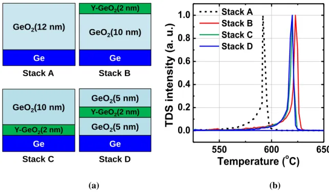
inverse direction. Both might be captured by the trap sites in the dielectric. Similar situation can be expected for negative Estress. (b) Vth shift as a function of electric field in Ge and Si stacks.50 ... 32 Figure 2.1 schematics of GeO desorption mechanism in GeO2/Ge stacks under thermal process.2 The GeO desorption process is accompanied by the VO formation and diffusion throughout the GeO2 layer, which result in drastic degradation of electrical properties... 43 Figure 2.2 Ellingham diagram for GeO2 and SiO2 formation under various oxygen ambient conditions calculated from thermodynamic data base.7 ... 44 Figure 2.3 ΔG0 for various metal oxides formation as a function of temperature. Note that the reaction formulas are normalized to one O2 molecule. ... 46 Figure 2.4 Y-GeO2/Ge gate stack preparation process by rf co-sputtered technics. Note that the annealing process of this gate stack is pure N2 ambient annealing in 1 atm pressure. .. 48
8
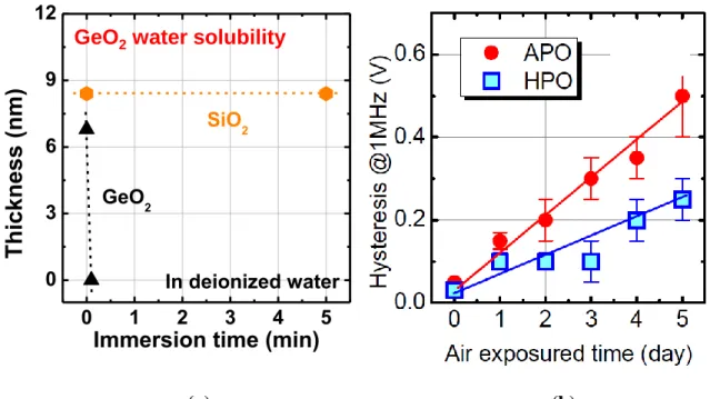
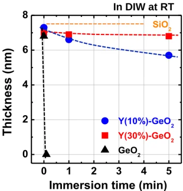
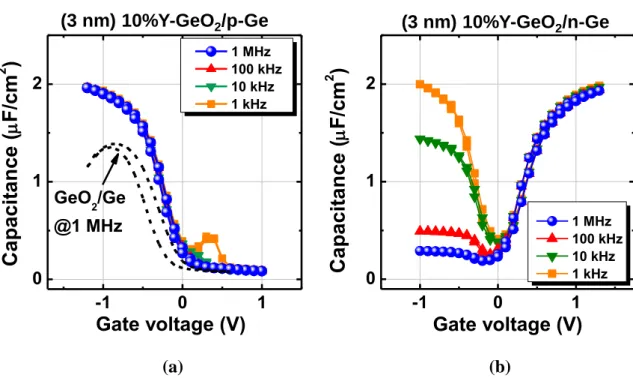
Figure 2.5 XPS core level spectra of Y3d and Ge3d from a Y-GeO2/Ge stack. The spectra are deconvoluted as shown in the dotted curves.12 ... 49 Figure 2.6 (a) Angle-resolved XPS spectra of Y-GeO2/Ge stack. The intensity ratio between Ge 3d 4+ and Y 3p is not changed by changing the take-off angle. (b) The atomic percentage of Y and Ge among metallic atoms calculated from the XPS spectra as a function of take-off angle. ... 50 Figure 2.7(a) TDS spectra corresponding GeO (m/z=90) from Y-GeO2/Ge and pure GeO2/Ge stacks. Note that the thicknesses of the dielectrics are 3 nm in these stacks. (b) TDS peak temperature corresponding to GeO as a function of initial Y-GeO2 and GeO2 thickness14 (the data of GeO2/Ge stack is re-plotted from ref. 2). Note that desorption of SiO from Si/SiO2 is also shown for comparison.15 The GeO desorption temperature is increased by the Y-doping. ... 51 Figure 2.8(a) Schematic of bilayer stacks with top Y doping (10%Y-GeO2/GeO2/Ge), bottom Y doping (GeO2/10%Y-GeO2/Ge) and in the middle. (b) Corresponding GeO desorption spectra. The spectrum of a 12 nm Ge/GeO2 stack is also shown as reference. 53 Figure 2.9 Thickness of GeO2 regrowth in (2 nm) Y-GeO2/Ge or GeO2/Ge stacks as a function of time under 550oC O2 ambient annealing. Regardless of the same initial thickness of Y-GeO2 and GeO2, the GeO2/Ge stack shows significant regrowth of GeO2, while Y-GeO2 can block the further oxidation. ... 54 Figure 2.10 Thickness of Y-GeO2 and GeO2 as a function of immersion time in pure DIW. The solubility of Y-GeO2 is drastically decreased. 14 Note that SiO2 is insoluble in water. 55 Figure 2.11 (a) Bidirectional C-V curves of an Au/10%Y-GeO2/p-Ge MOSCAPs measured at RT. The 1 MHz C-V curve of a sputtered (3nm) GeO2/p-Gestack is also shown for comparison. (b) Bidirectional C-V curves of Au/10%Y-GeO2/n-Ge MOSCAPs measured at RT. ... 56
9
Figure 2.12 Energy distribution of the estimated Dit in the Au/Y-GeO2/Ge stacks with various Y percentages measured by low-temperature conductance method. The state of art low Dit at GeO2/Ge interface prepared by HPO is also shown for comparison.8 ... 57 Figure 2.13(a) EOT as a function of Y-GeO2 and GeO2 physical thickness. It is notable that the enhancement of k-value is observed by Y-doping in GeO2.14 (b) JG as a function of Y-GeO2 and GeO2 physical thickness.14 ... 58 Figure 2.14(a) VFB as a function of the Y percentage in Y-GeO2/Ge stacks. A negative shift of the VFB from its ideal value is frequently observed in pure GeO2/Ge stacks, while Y doping can effectively alleviate this negative shift. Note that the thicknesses of the dielectrics are 3 nm in these gate stacks. (b). VFB of Y-GeO2/Ge stacks as a function of the physical thicknesses of Y-GeO2. A fixed charge density of 1×1011 cm-2 is derived from the slope of the line. ... 60 Figure 2.15 Schematics of amorphous GeO2 structure. The bond configurations of Ge and O atoms are also shown (2-dimensional represent). ... 61 Figure 2.16 Schematics of MRN structure of Y-GeO2. Due to the large amount of additional Y-O bond, some O atoms increase their coordination to 3 as well. ... 63 Figure 2.17 Network rigidity as a function of Nav estimated from the structures of Y-GeO2 and GeO2.29 The better rigidity of Y-GeO2 than the flexible GeO2 network results in its both better thermal stability and water resistance. Note that the γ value is assumed to be 0.8 here for all the GeO2 based oxides (γ=1 for SiO2). ... 64 Figure 2.18 FTIR absorbance spectra of pure GeO2 and Y-GeO2.14 The peak shift of asymmetric stretching mode in GeO2 to lower energy is clearly observed with the increase of Y concentration. The thickness of the dielectrics are 40 nm ... 65 Figure 2.19 TDS peak temperature of GeO desorption as a function of initial M-GeO2 and GeO2 thickness.12 The improvements of the thermal stability by different metal oxides doping, from lowest to highest, are in the order of Al2O3, HfO2, Sc2O3, Y2O3 and La2O3. 67
10
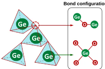
Figure 2.20 Thicknesses of M-GeO2 and pure GeO2 estimated from XPS as a function of immersion time in DIW.12 The water resistance increase by different metal oxides doping, from weakest to strongest, is Al, Hf, Sc, Y and La... 68 Figure 2.21 Expected coordination numbers of M cation in GeO2 network and the corresponding Nav of the total network.25, 26, 31 Note that the M percentage here is controlled to be 10% for all the M-GeO2 ... 69 Figure 2.22 (a) Tpeak and (b) Retching as a function of Nav. Note that the Tpeak are from the M-GeO2/Ge and GeO2/Ge stack with the same thickness (3 nm). Here, γ is assumed to be 0.8 for all the materials in the figure. ... 70 Figure 2.23 FTIR absorbance spectra of M-GeO2 and pure GeO2.12 The peak shift of asymmetric stretching mode in GeO2 to lower energy is clearly observed. The magnitude of this peak shift in different M-GeO2 is an indication of how strongly the GeO2 network is modified. ... 71 Figure 2.24 Bidirectional C-V curves of Au/GeO2/Ge and Au/M-GeO2/Ge MOSCAPs measured at RT: (a) GeO2, (b) Al-GeO2, (c) Hf-GeO2, (d) Sc-GeO2, (e) Y-GeO2, (f) La-GeO2.12 Note that the thicknesses of the dielectrics are about 3 nm in these gate stacks. ... 72 Figure 2.25 Energy distribution of Dit in M-GeO2/p-Ge and n-Ge stacks derived from low temperature conductance method (closed symbols) and high-low-frequency capacitance method (open symbols).12 It is notable that Y-GeO2 and Sc-GeO2 yield low Dit on Ge, which is close to the state-of-the-art low Dit at GeO2/Ge interface prepared by high-press oxidation.8 Hf-GeO2/Ge stack, on contrary, has a significantly higher Dit, especially in the lower half of Ge band gap. ... 73 Figure 2.26 Ge3d core level spectra of (a) Hf-GeO2/Ge and (b) Y-GeO2/Ge measured by XPS,12 Note that the spectrum of the as-cleaned Ge substrate is also shown in the dotted
11
line for comparison. The Ge-Hf metallic bond is preferentially observed in Hf-GeO2/Ge stack. (c) Schematic of the bond configurations in Y-GeO2/Ge and Hf-GeO2/Ge stacks.12 75 Figure 2.27 Dit at Ei-0.2 eV of Y-GeO2/Ge stacks as a function Y percentage. Though small amount of Y doping is beneficial in terms of low Dit, it increases a lot with high Y percentage. ... 77 Figure 2.28 Schematics of the degree of freedom and constrain of atoms in a network. The degree of freedom is related to the number of atoms, while the number of constraint is determined by the number of the bond. ... 78 Figure 2.29 AFM images of the top surface of (a) 10%Y-GeO2 and (b) 30%Y-GeO2 after 5 min immersion in DIW. The 10%Y-GeO2 is uniformly etched by water, while 30%Y-GeO2 shows some localized particles. ... 79 Figure 2.30 Phase diagram of GeO2-Y2O3 ternary oxide.41 Mainly three regions exist in the diagram, namely, Y-GeO2, Y-rich germanate and phase segregation region. ... 80 Figure 2.31. Schematic of two semi-empirical criteria for the interface properties in different M-GeO2/Ge stack. The doping species that are reactive with Ge substrate are in the red region and the unreactive ones are in the blue region. Note that part of the Ln RE cations are reactive with Ge. ... 82 Figure 3.1 Schematic of basic Ge gate stacks structure for EOT scaling into sub-nm region. The requirements on the ultra-thin IL and high-k are listed with regard to both IL and high-k. The issue for the IL has been addressed in the chapter 2. ... 91 Figure 3.2 Flowchart for the selection of thermally stable metal oxides on Si.8 In the triangular diagram, a solid line is plotted between every two materials which are not reactive with each other. ... 92 Figure 3.3 Experimal procedures to esitmate the intermixing thickness at the GeO2/Y2O3 interface. The critial point here is the different DIW etching rate between the intermixed layer and pure GeO2. ... 94
12
Figure 3.4(a) GeO2 thickness in GeO2/Y2O3/Ge stacks as a funtion of immersion time in diluted DIW. The results from a GeO2/Ge stack is also shown as a reference. The remained GeO2 layer after long time DIW etching is attributable to the intermixing between GeO2 and Y2O3 (Y-GeO2), which is not soluble in water. (b) The intermixing layer at GeO2/Y2O3 interface as a funtion of annealing temperature. ... 95 Figure 3.5 Bidirectional C-V curves of HfO2/Y-GeO2/Ge stacks with various Y-GeO2 IL thicknesses measured at RT. It is notable that decent C-V curves are kept with Y-GeO2 thickness over 1 nm, while thinner Y-GeO2 thickness (below 1 nm) results in the degradation of the C-V curve. The HfO2/(1 nm) GeO2/Ge stack also shows poor electrical properties. ... 96 Figure 3.6 Schematics of YScO3/Y-GeO2/Ge gate stack process. Note that in the step 3, low sputtering power is preferred to reduce damage to the passivated interface. ... 97 Figure 3.7(a) AFM image of the top surface of 4 nm YScO3/Ge stack after annealing. The RMS roughness is about 0.3 nm. (b) XDR pattern of (40 nm) YScO2/Ge gate stacks (both annealed and as-deposited). The XRD pattern of Ge(111) substrate are also shown for comparison. ... 98 Figure 3.8(a) EOT of YScO3/Y-GeO2/Ge gate stacks as a function of physical thickness of YScO3. Note that the physical thickness of Y-GeO2 IL is fixed at 1 nm, which contributes 0.5 nm in the total EOT. The inset shows the absorption coefficient (α) as a function of photon energy for a (40 nm) YScO3/Ge stack. (b) k and Eg values of Y2O3, Sc2O3 and YScO3. It is notable that YScO3 enhance the k-value comparing to its both binary compounds. ... 100 Figure 3.9(a) Refractive indices of Y2O3, Sc2O3 and YScO3 measured by spectroscopic ellipsometry on the (40 nm) Y2O3/Ge, Sc2O3/Ge and YScO3/Ge stacks, respectively. Note that the refractive indices are determined at λ=632 nm and α is assumed to be 0 at this
13
wavelength. The higher refractive index of YScO3 indicates a higher packing density. (b) Schematics of the coordination polyhedrons in Y2O3, Sc2O3 and YScO318, 19. ... 101 Figure 3.10 Densities of some REScO3 and that of their binary compounds. Note that the densities of REScO3 are higher than linear combination of their binary compounds, which indicates that they are more densely packed. ... 102 Figure 3.11 k-value of RE2O3, Sc2O3 and REScO3 as a function of αm/Vm (ref. 18-21). The k-value predicted by C-M equation is also shown as a reference. ... 103 Figure 3.12 XPS spectra from 4 nm YScO3/Ge gate stacks. The spectra are de-convoluted into Sc3p, Y4p and Ge3d peaks. Note that the spectra do not show obvious change with increasing the annealing temperature. ... 104 Figure 3.13 Dit at Ei-0.2 eV as a function of EOT in YScO3/Y-GeO2/Ge and HfO2/Y-GeO2/Ge stacks. Note that the thicknesses of both high-k dielectrics are fixed at 2 nm while the EOT is changed by Y-GeO2 IL thickness. HfO2 degrades the interface properties when Y-GeO2 IL is thinner than 1 nm. On contrary, YScO3 is immunity to interface degradation with ultra-thin Y-GeO2 IL. ... 105 Figure 3.14(a) Bidirectional C-V curves of YScO3/(0.5 nm)Y-GeO2/Ge gate stacks with EOT about 0.5 nm measured at RT.24 No hysteresis and frequency dispersion in C-V curves indicates that YScO3 does not degrade the Ge interface with only 0.5 nm Y-GeO2 IL. (b) JG as a function of EOT in YScO3/Y-GeO2/Ge gate stacks.24 Low JG is observed which is comparable to the state-of-the-art Ge gate stacks.14, 25-27 ... 106 Figure 3.15 Process flow and schematics of Ge n-MOSFET with YScO3/Y-GeO2/Ge gate stacks. 30 nm Y2O3 and 500 nm SiO2 were deposited to form the spacer and field oxides, respectively. Several channel lengths (W/L=90 μm/100–500 μm) were defined, and phosphorus (1×10¹⁵/cm2 dose) was implanted at 70 keV through the Y2O3 layer for source/drain (S/D) formation. (a) Y2O3 was etched with HCl-based solution to form spacer; Dopant activation was done by RTA at 600oC for 30 sec. (b) YScO3/Y-GeO2 deposition by
14
rf co-sputtering and annealed at 500oC N2/O2 (0.1%) for 30 sec. (c) Gate electrode patterning after Al deposition (d) S/D patterning. ... 107 Figure 3.16 The μeff of YScO3/Y-GeO2/Ge n-MOSFETs where the Y-GeO2 IL thickness is fixed at 1 nm. The μeff in the Y-GeO2/Ge n-MOSFET is also shown for comparison5. The peak μeff of 1057cm2/Vsec with EOT 0.8 nm is demonstrated in YScO3/Y-GeO2/Ge, which is the highest one in sub-nm EOT region due to the immunity to interface degradation. . 109 Figure 3.17 Benchmarking of peak electron mobility in Ge n-MOSFETs as a function of EOT.14, 24, 27, 30-32 Comparing to other conventional high-k, YScO3 shows moderate mobility degradation with reducing EOT... 110 Figure 4.1 Band diagram of Ge gate stacks with (a) electron or (b) hole trapping. Note that the black lines denote the ideal gate stack without trapping, while the blue and red dotted lines stands for the band distorted by electron and hole trapping, respectively. Such distortion of band is originated from the electric field from the trapped carriers, which is compensated by the shift of VG. ... 119 Figure 4.2 VFB shift of Al/SiO2/Si gate stack as a function of time under constant current stress of I=3×10⁻⁷ A (gate diameter=0.032 inch).16 For room temperature stress (293 K), the electron trapping is dominant initially and then the hole trapping becomes the major component. ... 120 Figure 4.3 Schematic of carrier injection model for trap generation in the dielectrics under a negative Estress.17 The electrons from the gate metal are accelerated by the external electric field and acquire the sufficient εgain to break the bond near interface. For the positive Estress, similar mechanism is involved except for that the holes are generated by the injected electrons. ... 121 Figure 4.4(a) Atomistic schematics of thermochemical model for dielectric degradation in SiO2.18, 20 The chemical bonds in the dielectric are broken by the Eloc (dependent on the dielectric thickness, VG and k-value) and the ions are displaced from the original sites,
15
which results in the generation of hole traps. (b) Schematically shows the energy states corresponding to the ideal dielectric and trap generation with and without electric field. 123 Figure 4.5 Schematics of the experimental procedures for Estress on Ge with both polarities. Note that the C-V curves are collected along the scan direction indicated by the arrows. 125 Figure 4.6(a) VFB shift in 1 atm GeO2/Ge stacks under 4 MV/cm Estress with both polarities. The large negative shift of the VFB represents the large amount of hole trapping. (b) The calculated energy level for VO in the GeO2/Ge gate stack,22 where GeOx is the transition region. Note that, regardless the dominant hole traps, certain amount of electron trap might also exists in the GeO2/Ge, which only observed under positive Estress with time longer than 300 sec (slightly positive VFB shift). ... 126 Figure 4.7 VFB shift in GeO2/Ge stacks with various process PO2 (1 to 70 atm) as a function of time under (a) positive and (b) negative Estress. The large negative VFB shifts are reduced in both polarities by increase PO2, which might be explained by less VO formation during the gate stack process. ... 128 Figure 4.8 VFB shift under circularly trapping-detrapping process by 900 sec of positive Estress and 10 sec of negative Estress. It is found that the trapping is highly repeatable under
both 2 and 4 MV/cm, which indicate that the trap generation can be neglected in these stress condition. ... 130 Figure 4.9 The newly generated electron trap density in GeO2/Ge stacks under positive Estress as a function of PO2 in the gate stack process. HPO can not sufficiently control the
trap generation under high Estress regardless of very promising properties in the initial and under low Estress field. ... 132 Figure 4.10 The newly generated electron trap density in Y-GeO2/Ge stacks as a function of Y percentage under positive Estress. Small amount of Y doping can drastically suppress the trap generation while high Y percentage degrades it again. ... 133
16
Figure 4.11(a) Electron trap generation calculated from the VFB shift in HPO-GeO2/Ge and M-GeO2/Ge stacks under positive high Estress (6.5 and 9 MV/cm). Note that the stress time
is fixed at 90 sec for a fair comparison. (b) Electron trap generation in HPO-GeO2/Ge and M-GeO2/Ge stacks under negative Estress calculated through the same way, while
breakdown occurs rapidly in HPO-GeO2/Ge stack under 9 MV/cm.28 ... 134 Figure 4.12 JG in (a) Y-GeO2/Ge, (b) Sc-GeO2/Ge, (c) Al-GeO2/Ge and (d) HPO-GeO2/Ge stacks with different stress time at 9 MV/cm positive Estress. Though HPO-GeO2 shows low initial JG, it increases a lot due to SILC. Y-GeO2 and Sc-GeO2 are stronger against SILC than HPO-GeO2 and Al-GeO2. Note that the applied field in JG measurement is also defined by VOX/EOT.28 ... 135 Figure 4.13 Dit at VFB (Ei-0.2 eV or Ei+0.17 eV for the p-Ge or n-Ge, respectively) increase in HPO-GeO2 and Y-GeO2/Ge stacks as a function of time under positive or negative 9 MV/cm Estress. Y-GeO2 can suppress the Dit generation compared to that of HPO-GeO2. ... 136 Figure 4.14 Dit at VFB increase after 90 sec stress for HPO-GeO2 and Y-GeO2/Ge stacks as a function of (a) Estress and (b) VOX. The VFB here is Ei-0.2 eV or Ei+0.17 eV for the p-Ge or n-Ge, respectively. Regardless of the X-axis, the smaller Dit generation in Y-GeO2/Ge stack can be confirmed in the viewpoint of both Estress and VOX. ... 137 Figure 4.15 Schematic of GeO2 network modification by Y or Sc doping (2-dimensional representation) and their influence on the ion displacement. The M-O bond number per cation is high for the doped M3+ in Y-GeO2 and Sc-GeO2,30, 31 result in the higher Nav of the
network. Under high Estress, the local bond breaking and consequent ion displacement occur in GeO2, while appropriate amount of additional M-O bonds enhance the rigidity of the network and suppress ion displacement.28 ... 139 Figure 4.16 (a) Bidirectional C-V curves of an Au/10% HPO-Y-GeO2/n-Ge MOSCAPs measured at RT. (b) Bidirectional C-V curves of Au/10% HPO-Y-GeO2/p-Ge MOSCAPs.
17
Note that the thickness of HPO-Y-GeO2 is 4 nm, which is the not changed by HPO annealing from the as deposited Y-GeO2. ... 141 Figure 4.17 VFB shift in HPO-Y-GeO2/Ge stack as a function of stress time at various stress condition (4, 6.5 and 9 MV/cm of (a) positive and (b) negative Estress). It is worth noting that the VFB shift in this gate stack is the smallest among all the gates stacks discussed in this chapter. ... 142 Figure 4.18 JG (absolute value) in HPO-Y-GeO2/Ge gate stack with different stress time at 9 MV/cm. The low initial JG reflects that HPO-Y-GeO2/Ge is an initially ideal gate dielectric. While the negligible SILC in this gate stack indicates its remarkably strong ability against trap generation. ... 143 Figure 4.19 Dit change in HPO-Y-GeO2/Ge stack as a function of stress time at various stress condition (4, 6.5 and 9 MV/cm of both polarities). The HPO-Y-GeO2/Ge is also the strongest gated stack against interface degradation among all the stacks reported in this work. ... 144 Figure 4.20 Hysteresis of the C-V curves in HfO2/Y-GeO2/Ge and YScO3/Y-GeO2/Ge stacks as a function of Y-GeO2 IL thickness. The references show the hysteresis of the Ge gate capacitances with GeOx as IL. 34, 35 ... 145 Figure 4.21 VFB shift in HfO2/Y-GeO2/Ge and YScO3/Y-GeO2/Ge stacks (EOT=0.8 nm) as a function of time under high negative VG (VG=1.5 and 2 V, Estress=10 and 15 MV/cm). The YScO3/Y-GeO2/Ge stacks show less VFB shift than the HfO2 counterpart at a fixed VG and EOT... 146 Figure 4.22 Dit at Ei-0.2 eV of YScO3/Y-GeO2/Ge and HfO2/Y-GeO2/Ge gate stacks as a function of time under 9 MV/cm negative Estress. The Dit at Y-GeO2/Ge stack is also shown for comparison. ... 147 Figure 4.23 Time to breakdown as a function of Estress in YScO3/Y-GeO2/Ge (EOT 0.8 nm), HfO2/Y-GeO2/Ge (EOT 0.8 nm) and Y-GeO2/Ge (EOT 2 nm) stacks. ... 148
18
List of tables
Table 1.1 scaling effect on the device parameters with device sized reduced by a factor K. Here α is a scaling factor which is larger than 1.13
... 22 Table 1.2 Basic physical properties of Ge and Si at 300 K.24 ... 26 Table 2.1 atom-atom distances in the GeO2 and Y-GeO2 network measured by EXAFS .. 66 Table 4.1 Trap densities of GeO2 and M-GeO2/Ge stacks estimated from the saturated VFB shift under 4 MV/cm Estress ... 129
19
Chapter 1
Introduction
1.1 High mobility channel material for future MOS device
1.2 Requirements for gate stack design in Ge MOS device
1.3 Objective and organization of this work
Chapter 1. Introduction
20
Overview
Due to the physical limitation on Si MOSFET dimensional scaling, Ge is emerging as an advanced channel material in substitute of Si to achieve higher device operation speed. The design of the gate dielectric is the most critical concern to ensure a sufficiently passivated Ge interface and high carrier mobility in the channel. Significant progresses have been reported recent years on the preparation of high quality GeO2 on Ge, which yield a well passivated Ge interface and high carrier mobility over Si universality. Though GeO2 has been believed to be the best candidate for the interface passivation, advanced gate dielectrics are still needed to improve several vital properties of Ge MOS device. Namely, the thermal and chemical robustness of the GeO2/Ge stack must be improved. The scalability of the equivalent oxide thickness to deep sub-nm region must be ensured. And finally, the long term reliability of the Ge MOS device must be evaluated. This work will investigate the various dielectrics oxides in terms of the above requirements. A structural viewpoint on dielectric oxides is to be developed for controlling the material and electrical properties of the Ge MOS device.
1.1 High mobility channel material for future MOS device
Since the first demonstration on silicon in 1959 by Dawon Kahng and Martin M Atalla in Bell Lab,1 metal-oxide-semiconductor field-effect-transistors (MOSFET) has been one of the most used electronic devices in the world. The logic, memory, power and radio-frequency (rf) circuits all utilize the MOSFET structure as their basic units.2-5 It is not hard to sketch a basic configuration of MOSFET (Figure 1.1).6 A MOSFET is basically an three-terminal device where the channel resistance between two contacts are controlled by the third.6 In detail, the carriers flow from the source to the drain, and the control terminal is the gate, which can manipulate the channel resistance by capacitively coupled
21
electric field. Despite this simple schematics of the MOSFET structure, the understanding and improvement the MOSFET are not easy challenges.
Figure 1.1 Schematics of a MOSFET with planar structure. There are three terminals for the device, the source, the drain and the gate. The carriers are injected from the source to the drain through the semiconductor channel, which is controlled by field applied through gate electrode.
Ever since the proposal of MOSFET concept in 1930s7, 8 and the first demonstration in 1959,1 progressive achievements have been made by the relentless works. In the recent decades of MOSFET researches, people have been focusing on shrinking the device size due to two fundamental reasons.9-12 Firstly, the smaller the devices are, the larger amount of them can be integrated in a circuit. With a fixed cost of entire wafer process, the average cost of a single function can be reduced by larger amount of devices. Secondly, the smaller device can offer faster switch delay for the logic function, thereby to achieve higher speed of the circuit. Table 1.1 lists in detail the size scaling results of the devices with constant electric field.13 With the shrinkage of the device size, the shorter switch delay, smaller power dissipation and larger number of transistors are obtainable, which is beneficial to
Semiconductor Source Drain Oxide Gate Source Drain Channel
Chapter 1. Introduction
22
improve the speed and the total number of functions on a single chip. Therefore, the scaling of the device size is the major trend for the MOSFET technology development for the recent decades.
Table 1.1 scaling effect on the device parameters with device sized reduced by a factor K. Here α is a scaling factor which is larger than 1.13
To utilize the aforementioned benefits of smaller devices, semiconductor enterprises have managed to reduce the device size by half in about every 3 years, following the prediction by Moore’s low.14
Figure 1.2 shows the international technology roadmap for semiconductors (ITRS) technology node of logic and memory devices,15 which basically reflects the half pitch scale of a single MOSFET. The blue squares represent the technology nodes which have already been achieved and the red circles are those expected in the near future.
Parameters
Expressions
Scaling
Saturated I
dI
d=V
satW
gC
ox(V
g-V
th)
K
I
d/gate wide
I
d/W
g1
Gate capacitance
C
g=ε
0ε
OXL
gW
g/t
OXK
Switch speed
τ=C
gV
dd/I
dK
Clock frequency
f=1/τ
1/K
Chip area
A
chipα
Integration
N
α/K
223
Figure 1.2 ITRS technology node of device scaling by years.15 The half reduction of the device dimensions has been successfully carried out every 3 years so far, but further reducing the device size to a few nm will inevitably face the physical limitations.
Regardless of the success on device scaling so far achieved, the simple reduction of devices size is no longer a viable choose for future since many intrinsic limitations emerge when the devices are in only several nm size. In the horizontal direction, short channel effect appears when the source and drain depletion regions take a substantial proportion of the channel length, featuring large source drain leakage current.6,16 In the vertical direction, to have sufficient control of the channel field by the gate bias, the thickness of the gate insulator is expected to be decreased with smaller device size, which inevitably results in a large gate leakage current (JG), limiting the further scaling of the oxide thickness.17, 18 Furthermore, the heavily doped source and drain region need to be more shallowly profiled with scaling of the device to maintain a high on current,18, 19 which is a great challenge for the doping technics concerning the solubility limitation. These intrinsic limitations,
1980 1990 2000 2010 2020 2030
10
010
110
210
3 FutureTech.
n
od
e (nm)
Year
Achieved Emerging physical limitationsChapter 1. Introduction
24
together with overwhelming production cost, make the further device size scaling virtually unattainable and useless.
Alternative approaches have been investigated to extend the semiconductor development in the More Moore era as summarized in Figure 1.3.13 These approaches are dealing with either device topology, gate insulator materials, or channel materials. Among them, replacing Si with high mobility (μ) semiconductors and replacing ploy-Si/SiO2 with metal gate/high-k dielectric might be a feasible choice for the MOSFET with high carrier mobilities and thin equivalent oxide thickness (EOT).
Figure 1.3 Schematics of various approaches to improve the device properties in the post dimensional scaling age.13 The device structure, gate insulator material and channel material are all possible components that can be improved.
Various high-μ semiconductors have been investigated20-23 to substitute Si as listed in Figure 1.4. Among them, germanium (Ge) has both high electron and hole mobilities over that of Si. It is notable that, though some group III-IV compound semiconductors have even higher electron mobilities, their hole mobilities are not satisfying. Thus, a balanced high electron and hole mobilities of Ge are a great advantage in terms of make the
25
complimentary MOS (cMOS) operations. Moreover, the low processing temperature of Ge makes it easier to be integrated in the existing Si technology. Therefore, Ge has emerged as the feasible channel material in replacement of Si.
(a) (b)
Figure 1.4 Bulk mobilities of (a) electron and (b) hole for various semiconductors. The striking advantage of Ge over the other semiconductor materials is that its electron and hole mobilities are higher than Si in a balanced way.
Ge is a lustrous, greyish-white matter in the group IVb in periodic table. It has five natural isotopes, namely, 70Ge, 72Ge, 73Ge, 74Ge and 76Ge. The structure of crystallized Ge is diamond structure in cubic phase, which is the same with that of crystallized Si. The other physical properties of Ge at room temperature (RT, 300K) are listed in Table 1.2 in comparison with Si.24
102 103 104 105 InSb InAs InP GaAs Ge El ec tron mobi lity (cm 2 /V s ) Si 10 2 103 104 105 InSb InAs InP GaAs Ge
Hole
mobi
lity
(cm
2/V
s
)
SiChapter 1. Introduction
26
Table 1.2 Basic physical properties of Ge and Si at 300 K.24
1.2 Requirements for gate stack design in Germanium MOS device
1.2.1 Intrinsically good interface of GeO2/GeTo ensure the high channel mobility, merely selecting a high-μ channel material is not enough, because the carriers in the channel are scattered by various mechanisms, namely, the Coulomb, phonon and surface roughness scatterings.25 Among them, the Coulomb scattering is dominating the channel mobility under a low field, and is largely determined by the selection of gate oxides. Because, without a sufficient passivation of the dielectric/Ge interface, a large density of interface states (Dit) might exist, which act as scattering source to limit the channel mobility.25 Therefore, the formation of a promising gate stack is one essential requirement for fully utilizing the high-μ of Ge. Germanium dioxide (GeO2) was naturally considered as the gate dielectric for Ge gate stack formation26 simply inspired by the successful SiO2/Si system. As expected, very promising interface properties has been obtained by the growth of high quality GeO2 through various methods thermally or chemically.27-29 The Dit can be controlled at about 1×10¹¹ eV-1cm-2 near the mid gap for these well prepared GeO2/Ge gate stack.27-29 Ge MOSFET operations have also been demonstrated with both electron and hole mobilities exceeding Si
Properties
Ge
Si
Density (g/cm
3)
5.323
2.329
Lattice constant (A)
5.658
5.431
Melting point (
oC)
937
1415
Dielectric constant
16.0
11.9
Band gap (eV)
0.66
1.12
Electron affinity, χ(V)
4.0
4.05
27
universality25 by GeO2/Ge interface as summarized in Figure 1.5. Besides GeO2, other dielectric materials with various deposition technics have also been investigated for Ge passivation, such as GeON,30 GeOS,31 fluorine,32 silicon,33 or direct high-k34-37 passivation. However, on contrary to GeO2/Ge interface, these passivation methods result in relatively higher Dit, which cannot yield high mobility for MOSFET operation. Therefore, we believed that GeO2 was the best candidate for Ge interface passivation so far.
Figure 1.5 Channel mobilities in Ge MOSFET reported in the literatures with high quality GeO2(x)/Ge interface27-29 or with other dielectric passivation.33-37 Both high electron and hole mobilities over that of Si universality25 have been demonstrated by GeO2/Ge interface. While with other passivation methods, the mobilities are relatively poorer.
1.2.2 Challenges for the Ge gate stack formation
Regardless of the promising properties of GeO2/Ge interface, there are still critical concerns on utilizing GeO2/Ge system for device application in a real scene. Firstly, GeO2 is a relatively soft material comparing to SiO2,38 which makes GeO2/Ge stacks thermally and chemically unstable. The formation of Ge monoxide (GeO) in the GeO2/Ge stack is
10
210
310
4 [33] GeO2 (GeOx) W/O GeO2 [35] Si UniversalityPea
k mobi
lity
(cm
2/Vs
)
Hole
[34]10
210
310
4 ref. 37Pea
k mobi
lity
(cm
2/Vs
)
GeO2 (GeOx) W/O GeO2 Si Universality ref. 27 ref. 28 ref. 29 ref.36Electron
ref. 33 ref. 34 ref. 35Chapter 1. Introduction
28
observed from a relatively low temperature as shown in Figure 1.6(a),39 which reflects the reaction between GeO2 and Ge. The formed GeO is then desorbed from the surface of GeO2/Ge stack and is detectable in the thermal desorption spectrum (TDS). Figure 1.6(b) shows the GeO desorption peak temperature from GeO2/Ge gate stacks as a function of initial thickness of GeO2 according to previous reports.40 GeO desorption occurs at a relatively low temperature, which is accompanied by the oxygen vacancy (VO) formation and electrical properties degradation.40
(a) (b)
Figure 1.6(a) GeO component in the GeO2/Ge gate stack as a function of annealing temperature.39 The inset shows the typical fit with six components due to three species, Ge, GeO and GeO2. Also shown in the inset is a plot of the intensity of the signal due to oxygen normalized by the beam current, indicating that the amount of oxygen remains essentially unchanged during the transformation. (b) GeO desorption peak temperature from GeO2/Ge stacks as a function of GeO2 thickness.40 The desorption temperature is quite low, especially for thin GeO2.
The highly hygroscopicity nature of GeO2 is also a big problem. Figure 1.7(a) shows the thickness of GeO2 as a function of immersion time in pure deionized water (DIW). On
29
contrary to water insoluble SiO2, several nm of GeO2 is immediately etched by DIW. The hygroscopic nature of GeO2 incurs not only great trouble in the device process but also reliability issue with exposure to air as shown in Figure 1.7(b).41 Both thermal instability and water solubility are among the biggest obstacles against bringing Ge back to future in spite of superior GeO2/Ge interface properties.
(a) (b)
Figure 1.7(a) The thickness of GeO2 and SiO2 as a function of immersion time in DIW. SiO2 is not etched by water, while GeO2 is etched immediately. (b) Hysteresis of the C-V curves of GeO2/Ge gate stack as a function of time with exposure to air.41 Regardless of the good initial properties, the hysteresis increase a lot with air exposure.
Since the dielectric constant (k) of GeO2 is about 5.2 to 5.9,26, 42 it is naturally hard for GeO2/Ge stack to achieve an EOT beneath 1 nm with affordable JG. Therefore, only ultra-thin GeO2 layer can be used as an interfacial layer (IL) between Ge and high-k dielectrics. The high-k/IL/Ge gate stack would be valid even for a real device application with very high switching frequency, because the high k-value is not reduced up to several
0 1 2 3 4 5 0 3 6 9 12 SiO2
Th
ickness
(n
m)
Immersion time (min)
GeO2In deionized water GeO2water solubility
Chapter 1. Introduction
30
tens of GHz.43 On the other hand, the biggest concern is the impact of high-k dielectrics on the interface. Due to the soft nature of GeO2, considerable intermixing might occurs between the top high-k dielectrics and the GeO2 IL in such bilayer stacks,44, 45 which makes the interface properties highly sensitive to the high-k dielectric as well. Most conventional high-k dielectrics are expected to form a defect state by intermixing into GeO2 IL as shown in Figure 1.8(a) (HfO2 on Ge in this example).46 Thus, the criteria for selecting proper high-k materials on sub-nm EOT Ge gate stack formation is more strict and comprehensive than that on Si. Without a proper high-k, the scaling of the EOT will inevitably be at the cost of Dit increase. This is the reason for the unsatisfying interface properties for very thin EOT Ge gate stack as reported in previous works (Figure 1.8(b) for a ZrO2 as high-k, which is very similar to HfO234). Therefore, selecting a proper high-k oxide with interface awareness becomes a key to the EOT scaling in sub-nm region.
(a) (b)
Figure 1.8(a) First principle calculations on the defect state formation when conventional high-k dielectric (HfO2 in this case) was intermixed with GeO2 IL.46 (b) Dit spectra of an aggressively scaled Ge stack with ZrO2 as high-k (similar to HfO2).34 Though very thin EOT is demonstrated, the Dit is in the order of 1012 cm-2eV-1 near the mid gap (almost 10
31
times higher than the state-of-the-art low Dit in Ge stack), which is not satisfying for high mobility MOSFET application.
Moreover, it is reported in the previous literatures that the higher k-value in the transition oxides are always at the cost of the smaller band gap as shown in Figure 1.9.47 For the low-k oxides like SiO2, the band gap can be as wide as 9 eV. While, for the ultra-high-k oxide TiO2, the band gap is only about 3 eV. The narrower band gap significant blurs the advantage of high-k dielectrics in terms of reducing JG. Thus it is a great challenge to find a suitable combination of high-k value and sufficient band gap.
Figure 1.9 Band gap of various oxides as a function of the k-value.46 The higher k-value is always at the cost of smaller band gap for normal transition metal oxides.
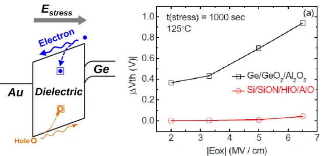
Finally, the promising initial characteristics of Ge MOS devices do not necessarily secure their long term reliability. Under an electric stress field (Estress), electron or hole are injected into the gate dielectric and might be captured by some trap sites in the dielectric, which results in the shift of device parameters over time as schematically shown in Figure 1.10(a).48, 49 The Dit or bulk trap density might also be increased by the Estress, which brings
Chapter 1. Introduction
32
about more severer shift of threshold voltage (Vth), the degradation of the trans-conductance (Gm) or the increase of JG. A comprehensive understanding is not yet obtained on the long term reliability properties of Ge MOS devices. The reports so far indicate that the trapping is much severer for Ge MOS than that of Si counterpart (Figure 1.10(b)).50 A systematic assessment on the Ge gate stack reliability is to be carried out to understand the reliability degradation mechanism and to improve the long term reliability projection.
Figure 1.10(a) Schematics of the carrier trapping in Ge MOS device under and positive Estress. The electrons are injected from the Ge to gate metal and the holes are injected in an
inverse direction. Both might be captured by the trap sites in the dielectric. Similar situation can be expected for negative Estress. (b) Vth shift as a function of electric field in Ge and Si stacks.50
1.3 Objective and organization of this work
In this work, I will focus on the gate stack formation on Ge in terms of aforementioned challenges. Under the presumption of (1) intrinsically good GeO2/Ge based interface, I will discuss the (2) improvement of the thermal and chemical robustness of the GeO2/Ge based
E
stressAu
Dielectric
Ge
33
interface. (3) design of an interface aware high-k for EOT scaling of Ge gate stack, and (4) understanding and improvement of the reliability of Ge gate stack for long term application. It is important to note that all the challenges should be addressed simultaneously and the solution of one issue should not be at the cost of sacrificing another. The approaches in this work are not simple optimization of process, but the research into entirely new materials which are intrinsically good for Ge MOS device application.
In the first chapter, inspired by thermodynamics on metal oxides, yttrium oxide doped GeO2 (Y-GeO2) is investigated for interface passivation on Ge. Significant improvement of both thermal stability and water resistance was demonstrated in GeO2/Ge stack by replacing GeO2 with Y-GeO2. The excellent electrical properties of Y-GeO2/Ge stack with low Dit are presented as well as the enhancement of k-value in Y-GeO2 layer, which is beneficial for further EOT scaling of Ge gate stack. Based on an systematic investigation of various metal oxides doping effect on GeO2, a structural modification model was proposed to explain the material properties change in metal oxide doped GeO2 (M-GeO2).
In the second chapter, the proper high-k dielectric is designed for EOT scaling into deep sub-nm. Since many conventional high-k oxides cause interface degradation when they are intermixed with GeO2 IL, the critical point here is to compromise the sufficient k-value with the awareness of the interface properties. An alternative approach for
designing high-k oxide is proposed in this chapter, namely the formation of a ternary real high-k out of two promising binary medium-k materials. As an example, yttrium scandate (YScO3) is demonstrated for gate stack formation on Ge, which enables the scaling down of the EOT to about 0.5 nm with affordable interface degradation. Ge n-MOSFET was also examined, which achieved the record high peak electron mobility (1057 cm2/Vsec) in the sub-nm EOT region.
In the third chapter, the reliability assessment was carried out on Ge gate stack with good initial properties. This work focuses on the trap density pre-existing in the
Chapter 1. Introduction
34
as-prepared gate stack and the degradation of the dielectric under a high Estress. It is found that though the initial trap density in the GeO2 is controllable by process condition, the degradation of the dielectric under high Estress is dominated by the intrinsically weak network of GeO2. The relatively rigid network materials like Y or Sc-GeO2 can suppress both interface degradation and trap generation under high Estress. The impact of different high-k on the reliability of Ge gate stack is also assessed.
Though the aforementioned challenges are solved separately in each chapter, the underlying physical understanding is in common. In a word, by manipulating the structure of the oxides, both the material and electrical properties of the oxides might be improved. In the final chapter, I will summarize such structure/property relationships for the oxides on Ge gate stack and offer a guideline for the Ge gate stack design in deep-nm EOT region.
35
References
1
D. Kahng, and M. M. Atalla, “Silicon–silicon dioxide field induced surface devices,” presented at the IRE Solid-State Device Res. Conf., Pittsburgh, PA, June 1960.
2
F. M. Wanlass, and C. T. Sah, “Nanowatt logic using field-effect metal-oxide semiconductor triodes,” in ISSCC Digest, p. 32, 1963.
3
D. Kahng and S. M. Sze, “A floating gate and its application to memory devices,” Bell Syst. Tech. J., vol. 46, p. 1288, 1967.
4
J. D. Pluer, and B. W. Scharf, “Insulated-gate planar thyristors: I-structure and basic operation,” IEEE Trans. Electron Devices, vol. 27, p. 380, 1980.
5
H. Itoh, T. Okabe, and M. Nagata, “Extremely high efficient UHF power MOSFET for handy transmitter,” IEDM Tech. Dig., p. 95, 1983.
6
S. M. Sze, and K. K. Ng, “Physics of semiconductor devices,” (Wiley, NJ, 2007) 3rd ed., chapter 6.
7
J. E. Lilienfeld, “Method and apparatus for controlling electric currents,” U.S. Patent 1,745,175. Filed 1926. Granted 1930.
8
O. Heil, “Improvements in or relating to electrical amplifiers and other control arrangements and devices,” British Patent 439,457. Filed and granted 1935.
9
H. Iwai, S.M. Sze, Y. Taur, and H. Wong “MOSFETs in guide to state-of-the-art electron devices,” (Wiley and IEEE, NJ, 2013), chapter 2.
10
H. Wong, “Nano-CMOS gate dielectric engineering,” (CRC Press, Boca Raton, 2012). 11
H. Wong, and H. Iwai, “The road to miniaturization,” Phys. World, vol. 18, p. 40, 2005. 12
H. Wong, and H. Iwai, “On the scaling of sub nanometer EOT gate dielectrics for ultimate nano CMOS technology,” Microelectronic Engineering, vol. 138, p. 57, 2015. 13
H. Iwai, “Roadmap for 22 nm and beyond,” Microelectronic Engineering, vol. 86, p. 1520, 2009.
Chapter 1. Introduction
36
14
R. R. Schaller, “Moore's law: past, present and future,” IEEE spectrum, vol. 34, 53, 1997.
15
International technology roadmap for semiconductors (ITRS), 2013 Edition, (http://www.itrs.net)
16
R. R. Troutman, “VLSI limitations from drain-induced barrier lowering,” IEEE Trans. Electron Devices, vol. 26, p. 461469, 1979.
17
B. Yu, H. Wang, C. Riccobene, Q. Xiang, and M.-R. Lin, “Limits of gate-oxide scaling in nano-transistors,” VLSI Symp. Tech. Dig., p. 90, 2000.
18
T. Ghani, K. Mistry, P. Packan, S. Thompson, M. Stealer, S. Tyagi, and M. Bohr, “Scaling challenges and device design requirements for high performance sub-50 nm gate length planar CMOS transistors,” VLSI Symp. Tech. Dig., p. 174, 2000.
19
Y. Taur, “CMOS design near the limit of scaling,” IBM J. RES. & DEV., vol. 46, p. 213, 2002.
20
C. O. Chui, H. Kim, D. Chi, B. B. Triplett, P. C. McIntyre, and K. C. Saraswat, “A Sub-400oC Germanium MOSFET technology with high-k dielectric and metal gate,” IEDM Tech. Dig., 437 (2002).
21
P. D. Ye, G. D. Wilk, J. Kwo, B. Yang, H.-J. L. Gossmann, M. Frei, S. N. G. Chu, J. P. Mannaerts, M. Sergent, M. Hong, K. K. Ng, and J. Bude, “GaAs MOSFET with oxide gate dielectric grown by atomic layer deposition,” IEEE Elec. Dev. Lett., vol. 24, p. 209, 2003. 22
Y. Q. Wu, Y. Xuan, T. Shen, P. D. Ye, Z. Cheng and A. Lochtefeld, “Enhancement-mode InP n-channel metal-oxide-semiconductor field-effect transistors with atomic-layer-deposited Al2O3 dielectrics,” Appl. Phys. Lett., vol. 91, p. 022108, 2007. 23
N. Li, E. S. Harmon, J. Hyland, D. B. Salzman, T. P. Ma, Y. Xuan, and P. D. Ye, “Properties of InAs metal-oxide-semiconductor structures with atomic-layer-deposited Al2O3 dielectric,” Appl. Phys. Lett., vol. 92, p. 143507, 2008.
37
24
Electronic archive new semiconductor materials characteristics and properties (http://www.ioffe.ru/SVA/NSM/)
25
S. Takagi, A. Toriumi, M. Iwase, and H. Tango, “On the universality of inversion layer mobility in Si MOSFET's: part I-effects of substrate impurity concentration,” IEEE Trans. Elec. Dev., vol. 41, p. 2357, 1994.
26
H. Matsubara, T. Sasada, M. Takenaka, and S. Takagi, “Evidence of low interface trap density in GeO2/Ge metal-oxide-semiconductor structures fabricated by thermal oxidation,” Appl. Phys. Lett., vol. 93, p. 032104, 2008.
27
A. Toriumi, C. H. Lee, S. K. Wang, T. Tabata, M. Yoshida, D. D. Zhao, T. Nishimura, K. Kita, and K. Nagashio, “Material potential and scalability challenges of germanium CMOS,” IEDM Tech. Dig., p. 646, 2011.
28
D. Kuzum, T. Krishnamohan, A. Nainani, Y. Sun, P. A. Pianetta, H.-S. P. Wong, and K. C. Saraswat, “High-mobility Ge n-MOSFETs and mobility degradation mechanisms,” IEEE Trans. Elec. Dev., vol. 58, p. 59, 2011.
29
R. Zhang, N. Taoka, P.-C. Huang, M. Takenaka, and S. Takagi, “1-nm-thick EOT high mobility Ge n- and p-MOSFETs with ultrathin GeOx/Ge MOS interfaces fabricated by plasma post oxidation,” IEDM Tech. Dig., p. 642, 2011.
30
H. Watanabe, K. Kutsuki, A. Kasuya, I. Hideshima, G. Okamoto, S. Saito, T. Ono, T. Hosoi, and T. Shimura, “Gate stack technology for advanced high-mobility Ge-channel metal-oxide-semiconductor devices -Fundamental aspects of germanium oxides and application of plasma nitridation technique for fabrication of scalable oxynitride dielectrics,” Curr. Appl. Phys. Lett., vol. 12, p. s10, 2012.
31
M. M. Frank, S. J. Koester, M. Copel, J. A. Ott, V. K. Paruchuri, and H. Shang, “Hafnium oxide gate dielectrics on sulfur-passivated germanium,” Appl. Phys. Lett.,vol. 89, p. 112905, 2006.
Chapter 1. Introduction
38
32
R. Xie, T. H. Phung, W. He, M. Yu, and C. Zhu, “Interface-engineered high-mobility high-k/Ge pMOSFETs with 1-nm equivalent oxide thickness,” IEEE Trans. Elec. Dev., vol. 56, p. 1330, 2009.
33
K. C. Saraswat, D. Kim, T. Krishnamohan, D. Kuzum, A. K. Okyay, A. Pethe, and H.-Y. Yu, “Germanium for high performance MOSFETs and optical interconnects,” ECS Trans., vol. 16, p. 3, 2008.
34
C.-M. Lin, H.-C. Chang, Y.-T. Chen, I.-H. Wong, H.-S. Lan, S.-J. Luo, J.-Y. Lin, Y.-J. Tseng, C. W. Liu, C. M. Hu, and F. L. Yang, “Interfacial layer-free ZrO2 on Ge with 0.39-nm EOT, κ~43, ~2×10⁻³ A/cm2 gate leakage, SS =85 mV/dec, Ion/Ioff =6×10⁵, and high strain response,” IEDM Tech. Dig., p. 509, 2012.
35
S. J. Whang, S. J. Lee, F. Gao, N. Wu, C. X. Zhu, J. S. Pan, L. J. Tang, and D.-L. Kwong, “Germanium p- & n-MOSFETs fabricated with novel surface passivation (plasma-PH3 and thin AIN) and TaN/HfOz gate stack,” IEDM Tech. Dig., p. 307, 2004.
36
W. P. Bai, N. Lu, A. Ritenour, M. L. Lee, D. A. Antoniadis, and D.-L. Kwong, “Ge n-MOSFETs on lightly doped substrates with High-k dielectric and TaN gate,” IEEE Elec. Dev. Lett., vol. 27, p. 175, 2006.
37
N. Wu, Q. Zhang, D. S. H. Chan, N. Balasubramanian, and C. Zhu, “Gate-first germanium nMOSFET with CVD HfO2 gate dielectric and silicon surface passivation,” IEEE Elec. Dev. Lett., vol. 26, p. 479, 2006.
38
E. N. Plotnikov, S. I. Lopatin, and V. L. Stolyarova, “Application of the sanderson method to the calculation of bonding energies in oxide glass-forming systems,” Appl. Phys. Lett., vol. 93, p. 161909, 2008.
39
K. Prabhakaran, F. Maeda, Y. Watanabe, and T. Ogino, “Distinctly different thermal decomposition pathways of ultrathin oxide layer on Ge and Si surfaces,” Appl. Phys. Lett., vol. 76, p. 2245, 2000.
39
40
S. K. Wang, K. Kita, C. H. Lee, T. Tabata, T. Nishimura, K. Nagashio, and A. Toriumi, “Desorption kinetics of GeO from GeO2/Ge structure,” J. Appl. Phys., vol. 108, p. 054104, 2010.
41
T. Nishimura, C. H. Lee, S. K. Wang, T. Tabata, K. Kita, K. Nagashio, and A. Toriumi, “Electron mobility in high-k Ge-MISFETs goes up to higher,” VLSI Symp. Tech. Dig., p. 209, 2010.
42
C. H. Lee, T. Tabata, T. Nishimura, K. Nagashio, K. Kita, and Akira Toriumi, "Ge/GeO2 interface control with high-pressure oxidation for improving electrical characteristics," Appl. Phys. Express vol. 2, p. 071404, 2009.
43
D. Barlage, R. Arghavani, G. Dewey, M. Doczy, B. Doyle, J. Kavalieros, A. Murthy, B. Roberds, P. Stokley, and R. Chau, “High-frequency response of 100 nm integrated CMOS transistors with high-k gate dielectrics,” IEDM Tech. Dig., p. 231, 2001.
44
S. Van Elshocht , M. Caymax, T. Conard, S. De Gendt, I. Hoflijk, M. Houssa, F. Leys, R. Bonzom, B. De Jaeger, J. Van Steenbergen, W. Vandervorst, M. Heyns, and M. Meuris, “Study of CVD high-k gate oxides on high-mobility Ge and Ge/Si substrates,” Thin Solid Film, vol. 508, p. 1, 2006.
45
N. Lu, W. Bai, A. Ramirez, C. Mouli, A. Ritenour, M. L. Lee, D. Antoniadis, and D. L. Kwong, “Ge diffusion in Ge metal oxide semiconductor with chemical vapor deposition HfO2 dielectric,” Appl. Phys. Lett., vol. 87, p. 051922, 2005.
46
G. Pourtois, M. Houssa, A. Delabie, T. Conard, M. Caymax, M. Meuris, and M. M. Heyns, “Ge 3d core-level shifts at (100)Ge∕Ge(Hf)O2 interfaces: A first-principles investigation,” Appl. Phys. Lett., vol. 92, p. 032105, 2008.
47
J. Robertson, “High dielectric constant gate oxides for metal oxide Si transistors,” Rep. Prog. Phys., vol. 69, p. 327, 2006.
48
D. J. DiMaria, E. Cat-tier, and D. Arnolda, “Impact ionization, trap creation, degradation, and breakdown in silicon dioxide films on silicon,” J. Appl. Phys., vol. 73, p. 3367, 1993.
Chapter 1. Introduction
40
49
M. Aoulaiche, M. Houssa, T. Conard, G. Groeseneken, S. De Gendt, and M.M. Heyns, “Impact of nitrogen incorporation in SiOx/HfSiO gate stacks on negative bias temperature instabilities,” Proceedings of IEEE International Reliability Physics Symposium, p. 317, 2006.
50
J. Ma, J.F. Zhang, Z. Ji, B. Benbakhti, M. Duan, W. Zhang, X.F. Zheng, J. Mitardc, B. Kaczer, G. Groesenekenc, S. Hall, J. Robertsone, P. Chalker, “Towards understanding hole traps and NBTI of Ge/GeO2/Al2O3 structure,” Microelectron. Eng., vol. 109, p. 43, 2013.
41
Chapter 2
Rigidity coordination in GeO
2
network
2.1 Thermodynamics for interface reaction and thin films
2.2 Enhancement of thermal stability and hygroscopic tolerance
in Y-GeO
22.3 Network modification model for metal oxide doped GeO
22.4 Concerns: interface defect bond and bulk immiscibility
Chapter 2. Rigidity coordination in GeO2 network
42
Overview:
The thermal and chemical robustness of the GeO2/Ge system is a vital concern in Ge gate stack formation. In this chapter, metal oxide doped GeO2 (M-GeO2) is proposed to substitute GeO2 for a robust IL formation in Ge stack according to the thermodynamic consideration. It is found that yttrium doped GeO2 (Y-GeO2) can improve the thermal stability of GeO2 by over 100oC and reduce the water etching rate of GeO2 by over 1000 times. The promising interface property comparable to the state-of-the-art GeO2/Ge is also demonstrated.
To consistently explain the improvement of thermal and chemical stability, the modification of GeO2 continuous random network (CRN) model is proposed, which build up a simple relationship between the network structure and various material and electrical properties. A systemic comparison on the material and electrical properties has also been carried out among different M-GeO2/Ge stacks to further examine the MRN model. Two criteria for selecting desirable doping materials in GeO2 are proposed. Firstly, metal cations with larger ionic radii are more preferable for their stronger influence on the GeO2 network rigidity, which result in the higher thermal stability and water resistance. Secondly, metal oxides are necessarily to be unreactive with Ge substrate (typically trivalent oxides) to prevent the Ge-M metallic bond formation.
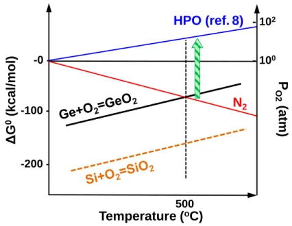
2.1 Thermodynamics for interface reaction and thin films
Regardless of its similarity with SiO2, GeO2 has been well known of its unstable thermal and chemical properties. It has been clarified that volatile germanium monoxide (GeO) are easily desorbed from GeO2/Ge stack at a relatively low temperature.1 Figure 2.1 schematically shows the GeO desorption mechanism from GeO2/Ge stacks under thermal process.2 It is notable that the GeO desorption involves the oxygen vacancy (VO) formation