Japan Advanced Institute of Science and Technology
JAIST Repository
https://dspace.jaist.ac.jp/Title
Flash-Lamp-Crystallized Polycrystalline Silicon Films with High Hydrogen Concentration Formed from Cat-CVD a-Si Films
Author(s) Ohdaira, Keisuke; Tomura, Naohito; Ishii, Shohei; Matsumura, Hideki
Citation Thin Solid Films, 519(14): 4459-4461
Issue Date 2011
Type Journal Article
Text version author
URL http://hdl.handle.net/10119/9833
Rights
NOTICE: This is the author's version of a work accepted for publication by Elsevier. Keisuke Ohdaira, Naohito Tomura, Shohei Ishii and Hideki Matsumura, Thin Solid Films, 519(14), 2011, 4459-4461, http://dx.doi.org/10.1016/j.tsf.2011.01.313 Description
1
Flash-Lamp-Crystallized Polycrystalline Silicon Films with High Hydrogen Concentration Formed from Cat-CVD a-Si Films
Keisuke Ohdaira1,2, Naohito Tomura1, Shohei Ishii1, and Hideki Matsumura1
1
Japan Advanced Institute of Science and Technology (JAIST), 1-1 Asahidai, Nomi,
Ishikawa 923-1292, Japan
2
PRESTO, Japan Science and Technology Agency (JST), 4-1-8, Honcho, Kawaguchi,
Saitama 332-0012, Japan
Abstract
We investigate residual forms of hydrogen (H) atoms such as bonding configuration in
poly-crystalline silicon (poly-Si) films formed by the flash-lamp-induced crystallization
of catalytic chemical vapor deposited (Cat-CVD) a-Si films. Raman spectroscopy
reveals that at least part of H atoms in flash-lamp-crystallized (FLC) poly-Si films form
Si-H2 bonds as well as Si-H bonds with Si atoms even using Si-H-rich Cat-CVD a-Si
films, which indicates the rearrangement of H atoms during crystallization. Peak
desorption temperature during thermal desorption spectroscopy (TDS) is as high as 900
ºC, similar to reported value for bulk poly-Si.
Keywords
Crystallization, Flash Lamp Annealing, Polycrystalline Silicon, Solar Cell, Catalytic
2
1. Introduction
Thin-film polycrystalline silicon (poly-Si) formed on low-cost substrates is a promising
material for next-generation solar cell because of its advantages of low material usage,
high stability against light soaking, and high performance. One of the methods of
forming such thin poly-Si films is crystallization of precursor a-Si films by annealing.
It has been demonstrated that poly-Si films formed by solid-phase crystallization
through hour-order furnace annealing can be processed to solar cells with conversion
efficiency of more than 10%, which indicates the feasibility of this concept [1]. To
realize higher throughput, rapid annealing techniques should be applied instead of
time-consuming furnace annealing.
Flash lamp annealing (FLA) is a millisecond-order annealing technique using pulse
emission from a Xe lamp array [2, 3], and can realize selective and sufficient heating of
micrometer-order-thick a-Si films and avoid thermal damage to entire low-cost glass
substrates. We have clarified that poly-Si films more than 4 µm thick can be formed
on quartz and soda lime glass substrates [4, 5]. No serious dopant diffusion occurs
during the flash-lamp-induced crystallization process [6], and diode and solar cell
operations have been demonstrated using flash-lamp-crystallized (FLC) poly-Si films
[7]. Catalytic chemical vapor deposition (Cat-CVD) is suitable as a method of
preparing precursor a-Si films for this purpose. This is because Cat-CVD can provide
a-Si films with low film stress [8], which results in the deposition of a-Si films more
than 4 µm thick without Si film peeling during deposition. Another advantage of
Cat-CVD for this purpose is the formation of a-Si films with moderately low hydrogen
(H) contents, which leads to the prevention of Si film peeling during deposition [9].
3
form FLC poly-Si films with H contents on the order of 1021 /cm3 [10, 11]. The
remaining H atoms can be utilized for the passivation of dangling bonds in FLC poly-Si
films [10-13]. We believe that the suppression of H desorption is due to explosive
crystallization, that is, lateral crystallization with velocity on the order of m/s triggered
by the release of latent heat [14, 15]. Fundamental understanding of the residual forms
of H atoms in FLC poly-Si films is important for the realization of more effective H
passivation using remaining H atoms. In this study, we have investigated the residual
forms of H atoms such as band configuration in FLA poly-Si films on the basis of
Raman spectroscopy and thermal desorption spectroscopy (TDS).
2. Experimental details
We first deposited a Cr film 200 nm thick on 20×20×0.7 mm3-sized quartz substrates by
sputtering, followed by the deposition of 4.5 µm-thick a-Si films by Cat-CVD.
Detailed deposition conditions for a-Si films have been summarized elsewhere [16].
FLA was performed under a fixed condition with pulse duration of 5 ms and irradiance
of approximately 20 J/cm2. Typical spectrum of flash lamp light can be seen
elsewhere [3]. Only one shot of flash lamp pulse was irradiated for each sample, and
no additional heating was supplied. No dehydrogenation process was performed prior
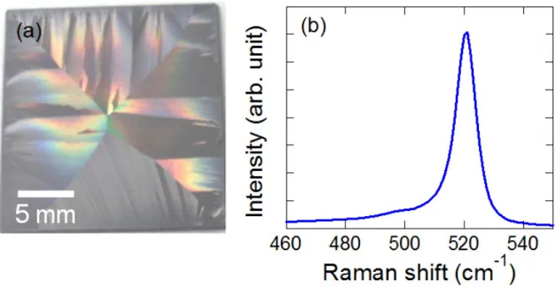
to FLA. Typical surface image and Raman spectrum of an FLC poly-Si film are
shown in Fig. 1.
TDS was performed both for an FLC poly-Si film and a precursor a-Si film. Each
sample was put on a holder in a high vacuum chamber (~10-8 Pa), and heated by
infra-red radiation from underneath at a heating rate of 10 °C/min from room
4
thermocouple embedded in the holder. Amount of desorbed H2 as a function of
temperature was detected with a quadrupole mass spectrometer. Relative amounts of
Si-H, Si-H2 and H-H bonds in a-Si and poly-Si films were evaluated by Raman
spectroscopy using a 632.8 nm light from a He-Ne laser.
3. Results and Discussion
Figure 2 shows the concentrations of H atoms in a precursor a-Si film and an FLC
poly-Si film estimated by TDS and secondary ion mass spectroscopy (SIMS) for
comparison. The TDS measurement reproduced H concentration in both films
previously obtained by SIMS [10,11], which indicates the accuracy of these
measurements. From these results, H contents are estimated to be 8% both for a-Si
and FLC poly-Si films, which is much larger than that obtained from the peak area of
the Si-H wagging mode in Fourier-transform infrared (FT-IR) spectrum (3-4%) of
Cat-CVD a-Si films. Similar tendency has been reported by other groups investigating
Cat-CVD a-Si films [17], and this phenomenon might be a character of Cat-CVD a-Si
films having H distribution different from plasma-enhanced CVD films [18].
Figure 3 shows TDS spectra of a precursor Cat-CVD a-Si film and a FLC poly-Si film.
One can see a clear peak at ~650 ºC, which is typically observed in TDS spectra of H2
from CVD a-Si films [19]. On the other hand, the spectrum of a FLC poly-Si shows
no clear desorption signals less than 600 °C, while the spectrum has a peak temperature
around 900 ºC. These features are completely different from that of an a-Si film, and
are rather similar to that of bulk poly-Si [20].
Figure 4 shows Raman spectra of a precursor a-Si film and a FLC poly-Si film for the
5
mainly seen in the spectrum of an a-Si film, whereas the Si-H2 peak, located at ~2090
cm-1, also appears after crystallization by FLA. On the other hand, H-H peak (~4158
cm-1 [21]) is not clearly observed in the Raman spectrum of an FLC poly-Si film.
These facts indicate that H atoms move and rearrange during FLA, and the final bond
configurations are mainly Si-H and Si-H2. We can imagine that the formation of Si-H2
bonds is unlikely inside crystalline Si grains, and most of them would exist at grain
boundaries and/or other defective parts.
One may expect that H atoms bonded to Si atoms as Si-H and Si-H2 will easily desorb
at 600 °C or less, as is the case for H atoms in a-Si films. However, surprisingly, we
can clearly see Si-H and Si-H2 signals in the Raman spectrum of an FLC poly-Si film
annealed at 700 °C for 30 min under N2 atmosphere, as shown in Fig. 4(b). Their
signal intensities are slightly smaller than the as-crystallized ones, but almost
comparable. This means that most of H atoms forming Si-H and Si-H2 bonds in FLC
poly-Si films do not completely desorb even at 700 °C, which is consistent with the
result of TDS measurement. Kisielowski-Kemmerich et al. have mentioned that the
peak temperature of as high as 900 °C for bulk poly-Si is due to the existence of
defective parts such as grain boundaries and/or dislocations [20]. This situation is also
applicable to FLC poly-Si films, which contain a number of 10-nm-sized fine grains
[14]. It is unlikely that the bonding energies of Si-H and Si-H2 in FLC poly-Si films
are widely different from those in a-Si films. Thus, the higher desorption temperature
of H atoms in FLC poly-Si films could be due to the trapping of temporarily unbonded
H atoms at defective parts which suppresses the outgassing of H atoms. Unbonded H
atoms would again form Si-H and Si-H2 bonds during cooling process. Further
6 mechanisms.
Finally we will discuss the impact of H residual forms on the termination of dangling
bonds by remaining H atoms. As mentioned above, grain boundaries could act to
suppress H desorption even at considerably high temperatures, which enables the
efficient rearrangement of H atoms during post-annealing of FLC poly-Si films.
Furthermore, since crystallization process by FLA is so immediate, unbonded H atoms
may also exist in FLC poly-Si films, although we have not confirmed their existence
because they cannot be detected by Raman spectroscopy. They could move to grain
boundaries or other defective parts during post-annealing, and would contribute to the
termination of Si dangling bonds, resulting in the significant improvement of minority
carriers lifetime and defect density reported previously [10, 11, 13].
4. Summary
H atoms in Cat-CVD a-Si films rearrange to form Si-H and Si-H2 bonds during
crystallization triggered by FLA. Most of H atoms do not desorb even annealing at
700 °C, and the peak desorption temperature is at around as high as 900 °C. This
phenomenon could be explained by the trapping of H atoms at grain boundaries or other
defective parts, which would leads to effective defect termination during post furnace
annealing.
Acknowledgments
The authors would like to thank T. Owada and T. Yokomori of Ushio Inc. for their
expert operation of FLA. The authors also acknowledge T. Yoshida of JAIST for his
7
References
1. M.J. Keevers, T.L. Young, U. Schubert, M.A. Green, 22nd European Photovoltaic
Solar Energy Conference, Milan, Italy, September 3-7, 2007, p. 1783.
2. B. Pécz, L. Dobos, D. Panknin, W. Skorupa, C. Lioutas, N. Vouroutzis, Appl. Surf.
Sci. 242 (2005) 185.
3. H. Habuka, A. Hara, T. Karasawa, M. Yoshioka, Jpn. J. Appl. Phys. 46 (2007) 937.
4. K. Ohdaira, Y. Endo, T. Fujiwara, S. Nishizaki, H. Matsumura, Jpn. J. Appl. Phys.
46 (2007) 7603.
5. K. Ohdaira, T. Fujiwara, Y. Endo, S. Nishizaki, H. Matsumura, Jpn. J. Appl. Phys.
47 (2008) 8239.
6. K. Ohdaira, T. Fujiwara, Y. Endo, K. Shiba, H. Takemoto, S. Nishizaki, Y.R. Jang, K.
Nishioka, and H. Matsumura, 33rd IEEE Photovoltaic Specialists Conference, San
Diego, U.S.A., May 11-16, 2008.
7. K. Ohdaira, T. Fujiwara, Y. Endo, K. Shiba, H. Takemoto, H. Matsumura, Jpn. J.
Appl. Phys. 49 (2010) 04DP04.
8. A.H. Mahan, Thin Solid Films 501 (2006) 3.
9. K. Ohdaira, K. Shiba, H. Takemoto, T. Fujiwara, Y. Endo, S. Nishizaki, Y.R. Jang, H.
Matsumura, Thin Solid Films 517 (2009) 3472.
10. K. Ohdaira, H. Takemoto, K. Shiba, H. Matsumura, Appl. Phys. Express 2 (2009)
061201.
11. K. Ohdaira, H. Takemoto, T. Nishikawa, H. Matsumura, Current Appl. Phys. 10
(2010) S402.
12. K. Brendel, N. H. Nickel, K. Lips, W. Fuhs, Mat. Res. Soc. Symp. Proc. 762 (2003)
8
13. K. Ohdaira, T. Nishikawa, S. Ishii, N. Tomura, K. Koyama, H. Matsumura,Proc. 5th
World Conf. Photovoltaic Energy Conversion (in press)
14. K. Ohdaira, T. Fujiwara, Y. Endo, S. Nishizaki, H. Matsumura, J. Appl. Phys. 106
(2009) 044907.
15. K. Ohdaira, T. Nishikawa, K. Shiba, H. Takemoto, H. Matsumura, Phys. Status
Solidi C 7 (2010) 604.
16. K. Ohdaira, S. Nishizaki, Y. Endo, T. Fujiwara, N. Usami, K. Nakajima, H.
Matsumura, Jpn. J. Appl. Phys. 46 (2007) 7198.
17. D.M. Goldie, S.K. Persheyev, J. Mater. Sci. 41 (2006) 5287.
18. A.H. Mahan, S.P. Ahrenkiel, R.E.I. Schropp, H. Li, D.S. Ginley, Thin Solid Films
516 (2008) 529.
19. P.J. Jennings, J.C.L. Cornish, B.W. Clare, G.T. Hefter, D.J. Santjojo, Thin Solid
Films 310 (1997) 156.
20. C. Kisielowski-Kemmerich, W. Beyer, J. Appl. Phys. 66 (1989) 552.
21. K. Murakami, N. Fukata, S. Sasaki, K. Ishioka, M. Kitajima, S. Fujimura, J. Kikuchi,
9
Figure captions
Fig. 1 (a) Typical surface image and (b) Raman spectrum of an FLC poly-Si film.
Fig. 2 H concentration in a precursor Cat-CVD a-Si film and an FLC poly-Si film
estimated by TDS and by SIMS [10, 11]. In the TDS measurement, H
concentrations were simply estimated using total amounts of effused H2
molecules and the volumes of Si films.
Fig. 3 TDS spectra of a precursor Cat-CVD a-Si film and a FLC poly-Si film.
Fig. 4 Raman spectra of a precursor a-Si film and a FLC poly-Si film for the
10
11
12
13