INVITED PAPER
Joint Special Section on Opto-electronics and Communications for Future Optical NetworkOptical absorption characteristics and polarization dependence of single-layer graphene on silicon waveguide
Kaori WARABI†a),Student Member, Rai KOU†,††,†††,Member, Shinichi TANABE††††, Tai TSUCHIZAWA††,†††, Satoru SUZUKI††††, Hiroki HIBINO†,Nonmembers, Hirochika NAKAJIMA†,Member, andKoji YAMADA††,†††,Senior Member
SUMMARY Graphene is attracting attention in electrical and optical research fields recently. We measured the optical absorption characteris- tics and polarization dependence of single-layer graphene (SLG) on sub- micrometer Si waveguide. The results for graphene lengths ranging from 2.5 to 200µm reveal that the optical absorption by graphene is 0.09 dB/µm with the TE mode and 0.05 dB/µm with the TM mode. The absorption in the TE mode is 1.8 times higher than that in the TM mode. An optical spectrum, theoretical analysis and Raman spectrum indicate that surface- plasmon polaritons in graphene support TM mode light propagation.
key words: graphene, silicon photonics, polarizer, optical absorption
1. Introduction
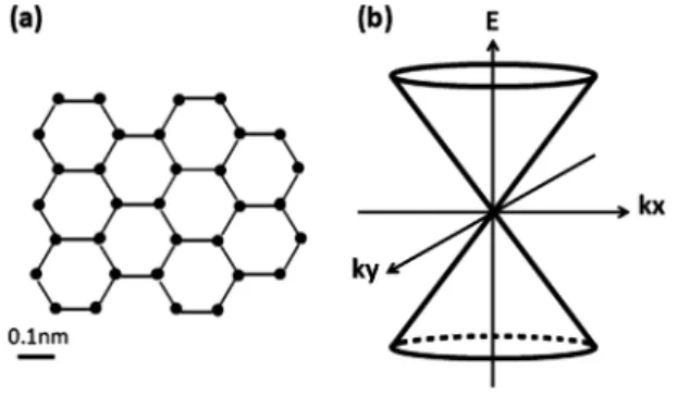
Graphene, a two-dimentional material with one-atom thick- ness [Fig. 1 (a)], is being investigated in electrical and optical research fields. Carbon atoms are strongly con- nected within each layer by covalent bonds of sp2 or- bitals, while they are connected weakly between layer with Van der Waals force. The interatomic distance and thick- ness are known to be 0.142 and 0.34 nm, respectively.
Graphene’s bandstructure has a unique shape as shown in Fig.1 (b), and graphene has various excellent characteristics [1]. In graphene, electrons are massless because of the lin- ear dispersion relationship between energy and momentum at around the Dirac point. As a result, graphene has very high mobility (over 10,000 cm2/Vs) and is thus attracting at- tention in the electrical research field. Moreover, graphene’s optical absorption is wavelength independent due to its zero band-gap structure, which enables us to fabricate broadband optical devices. This is the major reason it has recently at- tracted interest in the optical research field. Other excellent characteristics of graphene are a controllable band-gap in bi-layer graphene, high optical absorption efficiency (πα≈ 2.3% per layer), various nonlinear optical effects (for exam- ple, four-wave mixing and saturable absorption), and unique
Manuscript received November 14, 2013.
Manuscript revised January 30, 2014.
†The authors are with Graduate school of Advanced Sci- ence and Engineering, Waseda University, Shinjuku-ku, 169-8555 Japan.
††The authors are with NTT Nanophotonics center, NTT Cor- poration, Atsugi, 243-0918 Japan.
†††The authors are with Microsystem Integration Laboratories, NTT Corporation, Atsugi, 243-0198 Japan.
††††The authors are with Basic Research Labratories, NTT Cor- poration, Atsugi, 243-0198 Japan.
a) E-mail: [email protected] DOI: 10.1587/transele.E97.C.736
Fig. 1 (a) Molecular structure of graphene. (b)Band structure of graphene.
light propagation modes. These characteristics of graphene have been exploited in the development of various electri- cal and optical graphene devices, such as high-speed tran- sistors [2], THz light sources [3], fast photodetectors [4], high-efficiency modulators [5], and polarizers [6].
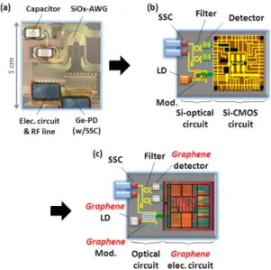
Recent advances in Si photonics enable us to imple- ment a hybrid integrated wavelength division multiplexing (WDM) receiver as shown in Fig. 2(a) [7]. The receiver comprises a Si waveguides, SiOx arrayed waveguide grat- ing, Ge photodetector, and electrical circuit on a 1×1 cm2 chip. It receives signal at 1.25 Gbit/s with 16 channels. In addition, monolithically integrated transceivers with Si pho- tonics technology will become widespread widely in the fu- ture [Fig. 2(b)]. In the transceivers, electrical and optical circuits are integrated on the same substrate, so a CMOS- compatible process is available, which strongly contributes to reducing fabrication costs. Since optical communica- tions technologies are progressing rapidly, faster, more ef- ficient, and smaller devices are required. However, previ- ously reported Si modulators based on the carrier-plasma- dispersion-effect have high power consumption and a large device area.
We assume that graphene can meet our expectations because it has many excellent characteristics as mentioned above, which enables the production of small-size devices with low power consumption. Small high-speed monolith- ically integrated transceivers with Si photonics technology and graphene [Fig. 2 (c)] will be implemented within 30 years [8].
Table 1 compares various Si and graphene modulators [9]–[14]. In Table 1, case 1 and 2 indicate 10 Gbit/s on-chip optical channels with 103 channels and 50 Gbit/s with 106 Copyright c⃝2014 The Institute of Electronics, Information and Communication Engineers
Fig. 2 Future vision of integrated devices. (a) WDM receiver with Si photonics. (b) Monolithically integrated transceiver with Si photonics. (c) Monolithic integrated transceiver with Si photonics and graphene.
Table 1 Device characteristics comparisons of various Si modulators and graphene modulator. Case 1 is on-chip optical channels whose speed and number of channels are 10 Gbit/s and 103channels. Case 2 is on-chip optical processing whose speed and number of channels are 50 Gbit/s and 106channels.
channels, respectively. The former can be implemented with Si photonics technology, but the latter is problematic and difficult to realize because of its huge power consumption and large area. Even if the most efficient modulation scheme with a reverse-biased Si-ring modulator is used, the power consumption reaches 60 kWh, which is three times what one person uses in a day in Japan [15], [16]. This problem could be mitigated by using graphene-based modulators, whose power consumption and area per chip are smaller than those with Si photonics technology only.
There are two reasons why a graphene modulator on a Si platform provides high efficiency. One is that a graphene modulator enables a high extinction ratio and wide band- width due to its high optical absorption efficiency per layer and high mobility compared with conventional materials.
Moreover, the Fermi level and optical absorption coeffi- cient can be controlled by applying a low swing voltage.
waveguides have not been investigated. In the Ref. [13], a graphene modulator on a Si waveguide was measured with only TE mode light; the optical absorption characteristics and polarization dependence of graphene were not charac- terized. Recently, we have transferred single-layer graphene with few defects onto Si waveguides and characterized its optical absorption efficiency in TE and TM mode polar- izations [17]. In this report, we describe additional infor- mation, including scanning electron microscopy (SEM) of single-layer graphene on a Si waveguide, propagation and coupling losses of Si waveguide and theoretical calculation of graphene’s conductivity to confirm mechanism of light propagation in graphene.
In this report, first, we will describe about device layout and fabrication in section 2. Next, we will show the results of micro-Raman spectroscopy and optical measurement in section 3 and 4. Finally, we will give some discussion in section 5 and conclude our research in section 6.
2. Device Layout and Fabrication
Before describing our device layout and fabrication pro- cess, we review the three main methods of graphene growth.
Graphene can be obtained by exfoliation from highly ori- ented pyrolytic graphite (HOPG) [18], by epitaxial growth on SiC substrate [19], and by chemical vapor deposition (CVD) on a transition metal such as Cu and Ni, which uses a catalyzed process [20]. Graphene obtained by exfoliating HOPG is smaller than 1,000µm2 and difficult to transfer to arbitrary positions, though it is high quality, nondoping and has high mobility (~10,000 cm2/Vs). However, to fab- ricate graphene-based optical devices, large-scale graphene is needed. To make multi-layer graphene, epitaxial growth on a SiC substrate is used. Large-scale graphene can be obtained by this method, but the mobility is low (~1,100 cm2/Vs) and there are relatively numerous defects. More- over, it is difficult to transfer graphene grown on SiC sub- strate to other substrates because of strong interaction be- tween graphene and its substrate. Compared to graphene grown by these two methods, graphene grown by CVD is large scale, easy to transfer onto arbitrary substrates, and has few defects. In addition, the mobility is higher (up to 4,050 cm2/Vs) than that of graphene grown by the epitaxy method, and it is easy to control the number of layers. For these rea- sons, CVD graphene is appropriate for use as a device ma- terial. If we use a Cu substrate, the low solubility of carbon
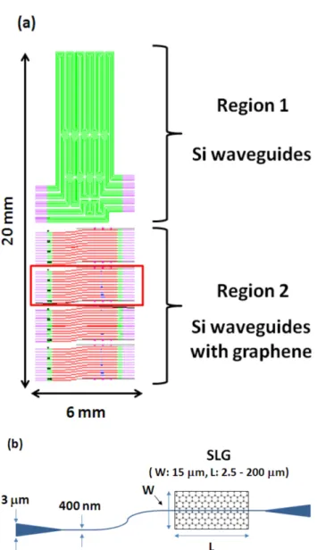
Fig. 3 (a) Top view of the chip. Region 1 is designed for measuring the propagation and coupling losses in Si waveguides, which have dif- ferent lengths. Region 2 is designed for measuring the absorption in the partly integrated graphene ranging from 2.5 to 200µm. (b) Top view of the graphene device.
in Cu helps self limiting in the growth process and single- layer graphene can be synthesized. On the other hand, few- layer graphene can be synthesized on Ni due to the high solubility of carbon. Direct graphene growth on Si substrate has also been investigated recently because of its simplicity, but single-layer graphene synthesis has not been achieved yet [21]. Therefore, CVD-grown graphene on Cu is suit- able for the fabrication of optical devices based on single- layer graphene, and we selected CVD-grown graphene for our fabrication process.
Our device layout on a 20 mm×6 mm chip is shown in Fig. 3 (a). Region 1 is Si waveguides without graphene integration, which is used to measure the propagation and coupling losses by varying the length of the waveguides.
Region 2 is Si waveguides with graphene integration, and an expanded view of the area enclosed by the square is
Fig. 4 Fabrication process. (a) PMMA was spincoated on a CVD-grown graphene on Cu substrate. (b) Cu substrate was etched with FeCl3solution.
(c) Graphene was transferred onto all Si waveguides on a 4-inch SOI wafer.
(d) PMMA was etched and graphene pattern was defined by photolithogra- phy and RIE. Cross section) Schematic of cross section of graphene device after all fabrication process.
shown in Fig. 3 (b). The line is a Si waveguide whose length, width and height are 6 mm, 400 nm, and 200 nm, respectively. We selected this width and height because they satisfy the single-mode propagation condition and yield evanescent light which has strong intensity at TE and TM polarizations. Tapered waveguides are formed at the in- put and output to reduce coupling losses. In this research, we were unable to form inverse taper spot size converters (SSCs) because the overclad process with electro cyclotron resonance-plasma chemical vapor deposition (ECR-CVD) damages graphene. The length of the single-layer graphene on Si waveguide is varied as 0, 2.5, 10, 20, 30, 50, 80, and 200µm and width is fixed at 15µm.
To fabricate the graphene device, we started from a 4-inch silicon on insulator (SOI) wafer (thickness of Si substrate, SiO2, and Si core are 525 µm, 3 µm and 200 nm, respectively). After a resist masked pattern had been formed by electron-beam (EB) lithography, Si chan- nel waveguides were precisely defined by electro cyclotron resonance-plasma ion etching (RIE) [22]. The fabrication process with graphene is shown in Fig. 4. First, we prepared 80×80-mm2thermal CVD grown single-layer graphene on a Cu substrate and cut it into pieces 30 ×30 mm2. Next, we spincoated PMMA film with thickness of several hun- dred nanometers to support the graphene [Fig. 4 (a)]. After that, we baked it at 170oC and etched the Cu substrate in ferric chloride (FeCl3) solution for over 12 hours at room temperature [Fig. 4 (b)]. Next, we rinsed the samples sev- eral times and transferred two sheets of graphene next to each other in deionized water to cover all Si waveguides on the wafer [Fig. 4 (c)]. Then, we dissolved the PMMA with acetone. Finally, we formed a 1.5-µm-thick photoresist and used photolithography and RIE with O2 gas to define the graphene patterns [Fig. 4 (d)].
3. Micro-Raman Spectroscopy
After transferring the graphene, we confirmed the quality and pattern accuracy of graphene by SEM observation and
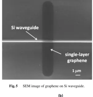
Fig. 5 SEM image of graphene on Si waveguide.
Fig. 6 Microscope image and micro-Raman spectroscopy (a) Micro- scope image of transferred single-layer graphene whose length is 2.5µm on Si waveguide. (b) Raman mapping of 2D band.
micro-Raman spectroscopy. An SEM image of 2.5-µm-long transferred graphene is shown in Fig. 5. We can observe that the transferred graphene has few cracks and the pat- tern is formed accurately. Then, we used 532-nm light as a pump and an objective lens of 50×to observe the trans- ferred graphene by micro-Raman spectroscopy. Figure 6 (a) shows an optical microscope image of 2.5-µm-long single- layer graphene on a Si waveguide. We selected the small- est graphene length to confirm that our fabrication process is sufficient for defining narrow graphene patterns. Fig- ure 6 (b) shows an expanded view of the area enclosed by the square together with Raman mapping of the 2D band (2695 cm−1). The bright area indicates the position of the graphene, which accurately reflects the photomask patterns as designed. Figure 7 shows the Raman-shift spectrum for measurement points 1 and 2 in Fig. 6. At point 1, the Ra- man characteristics of graphene appeared [23]. The D band (1350 cm−1), which represents the existence of defects al- most does not appear. In addition, information about the number of graphene layers can be attained from the peak intensity ratio of the G (1592 cm−1) and 2D bands. In this case, I(G)/I(2D) was approximately 0.25, so the transferred graphene is single layer. At point 2, the spectrum indi- cates that transferred graphene was perfectly etched in the un-masked region. From these results, we confirmed that transferred graphene is single layer with few defects and the graphene pattern is formed precisely. Additionaly, we also
Fig. 7 Raman-shift spectrum for measurement points 1 and 2.
Fig. 8 Optical measurement setup.
confirmed that the coverage of the single-layer graphene is over 90%, with hardly any multiple-layers or cracking.
4. Optical Measurement
We measured the optical absorption characteristics and po- larization dependence of single-layer graphene on a Si waveguide. The optical measurement setup is shown in Fig. 8. We used an amplified spontaneous emission (ASE) light source in the C-band (1530–1565 nm) and lensed fibers. Because the ASE light source has a large band- width, Fresnel reflection due to resonance can be prevented.
A high-input intensity may cause saturable absorption in graphene and two-photon-absorption induced free-carrier absorption in Si waveguide, so we set the on-chip coupled power to approximately 3 mW for the TE mode and 0.6 mW for the TM mode to avoid undesired nonlinear optical ef- fects. After polarization control with a polarizer and polar- ization controller, the input light was coupled into the de- vice. Optical absorption and spectrum of sample were mea- sured with a power meter and optical spectrum analyzer.
Figure 9 shows the results of a measurement. Optical absorptions by graphene in TE and TM modes are 0.09 and 0.05 dB/µm, which were evaluated from the slopes. We ob- tained a high extinction ratio per unit length of 0.04 dB/µm, which is the difference in optical absorption between the TE and TM modes.
Fig. 9 Measurement results for optical absorption and polarization de- pendence of graphene (The coupling loss is approximately 7 dB with the TE mode and 15 dB with the TM mode.).
Fig. 10 TE and TM mode spectra for graphene.
TE and TM mode spectra of 200-µm-long graphene are shown in Fig. 10. The spectra were obtained from the difference between the reference spectrum and that of the graphene-integrated Si waveguide at the same device length.
In the TM mode, a small decrease in absorption (1~2 dB) around 1550 to 1560 nm was observed, which can be ex- plained by slight nonlinear absorption in the reference Si waveguide. The spectrum range actually agrees well with the gain peak of the ASE light source, as shown in Ref.
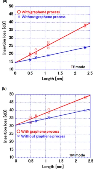
[17]. In addition, we measured the propagation and cou- pling losses of Si waveguides with and without the graphene process, as shown in Fig. 11 and Table 2. The propagation loss with the graphene process is twice as large as that with- out it. We suppose the cause of this is that a few graphene particles remain on the Si waveguide, which originate from the few-layer part of the transferred graphene. Note that the sidewall and top-surface roughness of the Si waveguide would be limited, because the etching time was quite short (only about several minutes). Moreover, the coupling loss for each port is very large, approximately 7 dB/facet with the TE mode and 15 dB/facet with the TM mode, and these val- ues are the same with and without graphene processes. We have to improve our transfer processes to prevent graphene
Fig. 11 (a) Loss of Si waveguide with and without graphene process (TE mode). (b) Loss of Si waveguide with and without graphene process (TM mode).
particles and design inverse tapers to reduce coupling losses [22].
5. Discussion
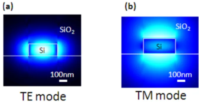
Since graphene interacts with propagating electric field, we simulated the mode profiles in a Si waveguide as shown in Fig. 12. The electric field of evanescent light in the TM mode is stronger than that in TE mode because of the flat- terned waveguide. We anticipated that optical absorption for the TM mode would be larger than that for the TE mode as a result of the very strong interaction between light and graphene. However, the results of the measurement were the opposite. Here, we focused on the spectra of the two polarization modes in graphene (Fig. 10). In the TE mode, absorption induced by graphene increases because the mode becomes larger as wavelength increases; the evidence indi- cates that TE mode light is simply absorbed by the graphene.
However, the absorption of TM mode light is wavelength independent, which is unusual. Here, we discuss the mech-
anism of TM mode absorption on the basis of a theoretical calculation.
Photoconductivity of graphene is represented by the sum ofσinterandσintrawhich are represented by
σinter(ω)= je2 4πℏln
2|µ| −(
ω+jτ−1) ℏ 2|µ|+(ω+jτ−1)ℏ
(1)
σintra(ω)= je2µ
πℏ2(ω+jτ−1) (2) where e is electric charge,ℏ=h/2πis the reduced Planck’s constant,µis the Fermi level (,0),ωis the radian frequency of input light whose wavelength is 1.55 µm, and τis the relaxation time of graphene [6]. If the imaginary part of σis negative, optical absorption of TM mode is large and propagation is mainly in the TE mode; if it is positive, the TM mode propagates mainly. We calculated the imaginary part of conductivity on Fermi level with Eqs. (1) and (2) as shown in Fig. 13 (We calculated withτ=10−12s) [24]–[26].
When the Fermi level is within±0.48 eV, the propagation is in the TE mode because the imaginary part of conductivity is negative. In band structure of graphene, the area is called an interband (|µ|≤ℏω/2). The interband transition occurs and the TE mode propagates. However, when the Fermi level is not around−0.4 or+0.4 eV, propagation is not a complete TE mode because the imaginary part of conductivity is ap- proximately zero. In the other range (|µ|> 0.48 eV), prop- agation is in the TM mode because the imaginary part of the conductivity is positive and the graphene acts as metal.
In the band structure of graphene, there is an area known as the intraband (|µ| >ℏω/2). In the intraband, free carriers and electric field interact and the TM mode propagates by means of surface plasmon polaritons, which strongly con- tribute to the low absorption in TM propagation compared with that in the TE mode [27].
Then, we estimated the Fermi level from the micro- Raman spectrum. As described in Ref. [28], the peak shifts of G and 2D bands occur as a result for an effect of car- rier doping in graphene. Comparing with Fig. 7 and Ref.
[28], we confirmed that the transferred graphene exhibits p- doping (Fermi level is approximately−0.4− −0.5 eV). It is supposed that the graphene acts as a metal and the propaga- tion is in the TM mode due to surface Plasmon polaritons.
Fig. 12 Simulation of electric field in Si waveguide without graphene integration. (a) TE mode. (b) TM mode.
Fig. 13 Imaginary part and real part of conductivity of graphene in units of e2/4ℏ. A solid line and dotted line indicates the imaginary and real part ofσ. Inset: Band structure of graphene.
It was reported that graphene on Si substrate becomes p-doped when it touches water because OH radicals bond with Si and promote carrier exchange [29]. The graphene would become p-doped during its transfer to a wafer.
Finally, we discuss the device’s working as a polarizer.
We obtained a four times higher extinction ratio (0.04 dB/ µm) than that in Ref. [6], in which the graphene was in- tegrated on a standard single-mode fiber (~10.6 dB/mm).
The advantage is that intensity of evanescent light of the Si waveguide is stronger. To obtain a 20-dB extinction ra- tio, millimeter-order graphene was required in Ref. [6], but in this work, we observed equivalent characteristics in graphene of several-hundred micrometers. The Fermi level of graphene exists on the boundary between TE and TM propagation in this work. We will be able to obtain a higher extinction ratio by changing Fermi level.
6. Conclusion
Single-layer graphene was successfully transferred to Si waveguides and the graphene pattern was formed precisely by RIE. We confirmed the optical absorption and polariza- tion dependence of single-layer graphene on a Si waveguide.
The results revealed that TE mode absorption is approxi- mately 1.8 times higher than that of TM mode because sur-
face plasmon polaritons support the TM mode. We suppose that if we add a gate oxidation layer and electrodes to the device, the polarization can be changed by applying gate voltage because the Fermi level of graphene changes. We expect to be able to fabricate a high-efficiency, controllable and ultra-small polarizer. The fundamental optical proper- ties of graphene, clarified in this report will contribute to the future development of graphene-integrated photonic de- vices.
Acknowledgement
The authors thank Mr. T. Watanabe of NTT Advanced Tech- nology for technical assistance, and Dr. C. M. Orofeo, Dr.
H. Fukuda and Mr. H. Nishi of NTT Laboratories for helpful discussions.
References
[1] F. Bonaccorso, Z. Sun, T. Hasan, and A. C. Ferrari, “Graphene pho- tonics and optoelectronics,” Nat. Photonics, vol. 4, no. 9, pp. 611–
622, Aug. 2010.
[2] L. Liao, Y. C. Lin, M. Bao, R. Cheng, J. Bai, Y. Liu, Y. Qu, K.
L. Wang, Y. Huang, and X. Duan, “High-speed graphene transis- tors with a self-aligned nanowire gate,” Nature, vol. 467, no. 7313, pp. 305–308, Sept. 2010.
[3] V. Ryzhii, A. A. Dubinov, T. Otsuji, V. Mitin, and M. S. Shur, “Tera- hertz lasers based on optically pumped multiple graphene structures with slot-line and dielectric waveguides,” J. Appl. Phys., vol. 107, no. 5, pp. 054505, Mar. 2010.
[4] F. Xia, T. Mueller, Y. Lin, A. Valdes-Garcia, and P. Avouris, “Ul- trafast graphene photodetector,” Nat. Nanotech. vol. 4, pp. 839–843, Oct. 2009.
[5] G.-C. Lee, S. Suzuki, W. Xie, and T. R. Schibli, “Broadband graphene electro-optic modulators with sub-wavelength thickness,”
Opt. Express, vol. 20, no. 5, pp. 5264–5269, Feb. 2012.
[6] Q. Bao, H. Zhang, B. Wang, Z. Ni, Y. Wang, D. Y. Tang, and K. P.
Loh, “Broadband graphene polarizer,” Nat. Photon., vol. 5, no. 7, pp. 411–415, May 2011.
[7] H. Nishi, T. Tsuchizawa, R. Kou, H. Shinojima, T. Yamada, H.
Kimura, Y. Ishikawa, K. Wada, and K. Yamada, “Monolithic inte- gration of a silica AWG and Ge photodiodes on Si photonic platform for one-chip WDM receiver,” Opt. Express, vol. 20, no. 8, pp. 9312–
9321, Apr. 2012.
[8] K. S. Novoselov, V. I. Fal’ko, L. Colombo, P. R. Gellert, M. G.
Schwab, and K. Kim, “A roadmap for graphene,” Nature, vol. 490, no. 7419, pp. 192–200, Oct. 2012.
[9] P. Dong, S. Liao, D. Feng, H. Liang, D. Zheng, R. Shafiiha, C.
Kung, W. Qian, G. Li, X. Zheng, A. V. Krishnamoorthy, and M.
Asghari, “Low Vpp, ultralow-energy, compact, high-speed silicon electro-optic modulator,” Opt. Express, vol. 17, no. 25, pp. 22484–
22490, Dec. 2009.
[10] W. M. J. Green, M. J. Rooks, L. Sekaric, and Y. A. Vlasov, “Ultra- compact, low RF power, 10 Gb/s silicon Mach-Zehnder modulator,”
Opt. Express, vol. 15, no. 25, pp. 17106–17113, Dec. 2007.
[11] A. Liu, L. Liao, D. Rubin, H. Nguyen, B. Ciftcioglu, Y. Chetrit, N. Izhaky, and M. Paniccia, “ High-speed optical modulation based on carrier depletion in a silicon waveguide,” Opt. Express, vol. 15, no. 2, pp. 660–668, Jan. 2007.
[12] Q. Xu, S. Manipatruni, B. Schmidt, J. Shakya, and M. Lipson,
“12.5 Gbit/s carrier-injection-based silicon micro-ring silicon mod- ulators,” Opt. Express, vol. 15, no. 2, pp. 430–436, Jan. 2007.
[13] M. Liu, X. Yin, E. Ulin-Avila, B. Geng, T. Zentgraf, L. Ju, F. Wang, and X. Zhang, “A graphene-based broadband optical modulator,”
Nature, vol. 474, no, 7349, pp. 64–67, June 2011.
[14] S. J. Koester, H. Li, and M. Li, “Switching energy limits of waveguide-coupled graphene-on-graphene optical modulators,”
Opt. Express, vol. 20, no. 18, pp. 20330–20341, Aug. 2012.
[15] International Energy Agency,
http://www.iea.org/stats/prodresult.asp?PRODUCT=Electricity/ Heat, 2008
[16] Central Intelligence Agency, “The world factbook,”
https://www.cia.gov/library/publications/download/, 2009.
[17] R. Kou, S. Tanabe, T. Tsuchizawa, K. Warabi, S. Suzuki, H. Hibino, H. Nakajima, and K. Yamada, “Characterization of optical absorp- tion and polarization dependence of single-layer graphene integrated on a silicon wire waveguide,” Jpn. J. Appl. Phys., 52, pp. 060203, May 2013.
[18] K. S. Novoselov, A. K. Geim, S. V. Morozov, D. Jiang, Y. Zhang, S. V. Dubonos, I. V. Grigorieva, and A. A. Firsov, “Electric field effect in atomically thin carbon films,” Science, vol. 306, no. 5696, pp. 666–669, Oct. 2004.
[19] C. Berger, Z. Song, T. Li, X. Li, A. Y. Ogbazghi, R. Feng, Z. Dai, A. N. Marchenkov, E. H. Conrad, P. N. First, and W. A. de Heer,
“Ultrathin epitaxial graphite: 2D electron gas properties and a route toward graphene-based nanoelectronics,” J. Phys. Chem. B, vol. 108, no. 52, pp. 19912–19916, Oct. 2004.
[20] X. Li, W. Cai, J. An, S. Kim, J. Nah, D. Yang, R. Piner, A. Vela- makanni, I. Jung, E. Tutuc, S. K. Banerjee, L. Colombo, and R. S.
Ruoff, “Large-area synthesis of high-quality and uniform graphene films on copper foils,” Science, vol. 324, no. 5932, pp. 1312–1314, June 2009.
[21] D. Wei and X. Xu, “Laser direct growth of graphene on silicon sub- strate,” Appl. Phys. Lett., vol. 100, no. 2, pp. 023110, Jan. 2012.
[22] T. Tsuchizawa, K. Yamada, H. Fukuda, T. Watanabe, J. Takahashi, T. Shoji, E. Tamechika, S. Itabashi, and H. Morita, “Microphotonics devices based on silicon microfabrication technology,” IEEE J. Sel.
Top. Quantum Electron., vol. 11, no. 1, pp. 232–240, Jan. 2005.
[23] L. M. Malard, M. A. Pimenta, G. Dresselhaus, and M. S. Dressel- haus, “Raman spectroscopy in graphene,” Phys. Rep., vol. 473, no.
5–6, pp. 51–87, Apr. 2009.
[24] J. M. Dawlaty, S. Shivaraman, M. Chandrashekhar, F. Rana, and M.
G. Spencer, “Measurement of ultrafact carrier dynamics in epitaxial graphene,” Appl. Phys. Lett., vol. 92, no. 4, pp. 042116, Jan. 2008.
[25] V. P. Gusynin, S. G. Sharapov, and J. P. Carbotte, “Unusual mi- crowave response of Dirac quasiparticles in graphene,” Phys. Rev.
Lett., vol. 96, no. 25, pp. 256802, June 2006.
[26] S. A. Mikhailov and K. Ziegler, “New electromagnetic mode in graphene,” Phys. Rev. Lett., vol. 99, no. 1, pp. 016803, July 2007.
[27] S. A. Mikhailov, “Theory of the giant plasmon-enhanced second-harmonic generation in graphene and semiconductor two- dimensional electron systems,” Phys Rev. B, vol. 84, no. 4, pp. 045432, July 2011.
[28] A. Das, S. Pisana, B. Chakraborty, S. Piscanec, S. K. Saha, U. V.
Waghmare, K. S. Novoselov, H. R. Krishnamurthy, A. K. Geim, A.
C. Ferrari, and A. K. Sood, “Monitoring dopants by Raman scat- tering in an electrochemically top-gated graphene transistor,” Nat.
Nanotechnol., vol. 3, no. 4, pp. 210–215, Mar. 2008.
[29] M. Lafkioti, B. Krauss, T. Lohmann, U. Zschieschang, H. Klauk, K. V. Klitzing, and J. H. Smet, “Graphene on a hydrophobic sub- strate: doping reduction and hysteresis suppression under ambient conditions,” Nano. Lett., vol. 10, no. 4, pp. 1149–1153, Mar. 2010.
gineers of Japan and IEEE.
Rai Kou received the B.E. and M.E. de- grees in applied physics from Waseda Univer- sity, Tokyo, Japan, in 2007 and 2009, respec- tively. From 2007 to 2009, he was a Visiting Re- search Student at the National Institute for Ma- terials Science (NIMS), Tsukuba, Japan, where he was engaged in nonlinear optics. He has been at NTT Microsystem Integration Laborato- ries since 2009, and NTT Nanophotonics Center since 2012 (concurrent post), Atsugi, Japan. His current research interests focus on integrated photonic circuits with silicon and its related materials.
Mr. Kou is a member of the Japan Society of Applied Physics (JSAP), the Institute of Electronics, Information and Communication Engineers (IE- ICE), and IEEE.
Shinichi Tanabe received the B.E. and M.E.
degrees in materials engineering from Osaka University in 2007 and 2009, and the Ph.D. de- gree in physics from the University of Tsukuba in 2013. In 2009, he joined Basic Research Laboratories, NTT Corporation. He is engaged in research on the transport properties of SiC graphene. He is a member of the Japan Society of Applied Physics.
Tai Tsuchizawa received the B.S. and M.S. degrees in physics from Sophia Univer- sity, Tokyo, Japan, in 1984 and 1986, respec- tively, and the Ph.D. degree from the Univer- sity of Tokyo, Japan, in 1990. Currently, he is a Senior Research Engineer in NTT Microsys- tem Integration Laboratories, Atsugi, Japan. In NTT’s laboratories, he has engaged in studies on plasma process for microfabrication. His current research interest is fabrication technolo- gies for silicon-based optoelectronics devices.
Dr. Tsuchizawa is a Member of the Japan Society of Applied Physics.
Hiroki Hibino received his B.S. (1987) and M.S. (1989) in physics from the University of Tokyo and a Ph.D. (2006) in Pure and Applied Physics from Waseda University.
Currently, he is Executive Manager of the Mate- rials Research Laboratory and Group Leader of the Low-dimensional Nanomaterials Research Group at NTT Basic Research Laboratories. His research interests include step structures on vic- inal surfaces, surface mass transport, step in- stability during epitaxial growth, self-assembled nanostructure formation, and epitaxial graphene growth. He spent one year as a visiting research professor at Arizona State University, 2000–2001. He also has experience as a visiting professor at the Tokyo Institute of Technol- ogy (2007–), Kyushu University (2009–2010), and the University of Tokyo (2011–).
Hirochika Nakajima received the B.E., M.S. and Dr.Eng. degrees from Waseda Univ.
In 1972, he joined Fujitsu Labs. Ltd,
where he engaged in R&D of magnetic and opti- cal devices. In 1996, he moved to Waseda Univ.
as a full professor of applied physics. From 2004 to 2006, he was with CRDS at JST as a so- called rotator in Japanese government agency.
After that, he occupied the position of director for research promotion and research strategy at his university. He is one of founders of the Mi- crooptics Conference (MOC) and has been a program committee member since 1987. He received a Microotics Contribution Award and the 9th K.
Sakurai Memorial Award in 2009 and 1993, respectively. He is a member of JSAP (fellow)/OSJ and IEICE. He has been the managing chair of the Microoptics Group, since 2001.
Koji Yamada received his B.E., M.E.
and Ph.D. degrees in nuclear engineering from Kyushu University, Japan, in 1986, 1988 and 2003, respectively. He joined NTT in 1988, and is now a Senior Research Engineer, Super- visor, Distinguished Technical Member in NTT Nano-Photonics Center and NTT Microsystem Integration Laboratories. In NTT laboratories, he was engaged in studies on synchrotron light sources, and since 2000 he has been engaged in studies on silicon photonic platform. From 2010, he is also a leader of photonic wiring and waveguide research team of PECST project supported by the JSPS, Japan. He is a member of the Japan Society of Applied Physics, the Atomic Energy Society of Japan, the Particle Accelerator Society of Japan, the IEICE and IEEE.