九州大学学術情報リポジトリ
Kyushu University Institutional Repository
Studies on CVD Growth of Single-Crystal Graphene on Cu Foil
丁, 冬
https://doi.org/10.15017/1866327
出版情報:九州大学, 2017, 博士(工学), 課程博士 バージョン:
権利関係:
i
Studies on CVD Growth of Single-Crystal Graphene on Cu Foil
A Dissertation Presented to
the interdisciplinary Graduate School of Engineering Sciences of Kyushu University
Dong DING
2017
ii
Abstract
Graphene has attracted a widespread interest due to its unique electrical and mechanical properties.
Large-area monolayer graphene can be produced by chemical vapor deposition (CVD) on Cu surface with a relatively low cost. However, CVD-grown graphene is composed of merged small grains separated by graphene grain boundaries (GGBs), which degrade the properties of graphene. Controlling the position of the nucleation during the growth can allow obtaining single-crystal graphene grain without GGBs.
However, it is still a challenge to precisely control the nucleation sites on Cu foil. In this thesis, I propose a novel method and show how Ni foils strategically placed in the CVD process enable the growth of a spatially defined nucleation of mm-scale, pure monolayer single-crystal grain graphene. This is done by locally tuning the CH
4feedstock with the catalytically active Ni foils. Apart from the site-selective graphene growth, this method also allows to directly grow patterned graphene without any lithography processes.
For the site-selective growth of graphene mentioned above, I employed pre-oxidized Cu foil to reduce the graphene nucleation density, by heating it up from room temperature (RT) to the target temperature in Ar. However, the mechanism behind this decrease in the nucleation density remains unclear. In this thesis, I investigated the changes in the copper oxide layer during the different steps of the CVD process by flowing gases with different compositions. The remaining oxygen in the subsurface of the Cu foil after heating up in Ar was found to be essential to decrease the nucleation density of graphene.
Finally, nondestructive characterization of graphene by dark-field (DF) optical microscope is studied.
GGBs on Cu foil can be quickly identified by the enhanced contrast from DF images, thanks to the
scattering light by copper oxide nanoparticles and Cu steps below the graphene. The evaluation of oxygen
resistance for graphene-coated Cu was also performed by using DF optical microscope. It was found that
the dissolved oxygen in oxygen-rich Cu plays an important role on the accelerated oxidation. I believe that
the results presented in this thesis will boost the realization of large-area and high-quality single crystal
graphene applicable in industry in the future.
iii
Table of contents
Abstract
Chapter 1: Introduction ... 1
1.1. History of graphene... 1
1.2. Applications ... 3
1.3. Motivation and purpose ... 3
1.4. Outline of thesis ... 4
1.5. References ... 5
Chapter 2: Graphene ... 9
2.1. Carbon atoms ... 9
2.2. Fundamental of structural and electronic properties of graphene ... 11
2.3. Preparation of graphene ... 15
2.3.1. Mechanical cleavage and exfoliation ... 15
2.3.2. Chemical cleavage and exfoliation ... 17
2.3.3. Synthesis on SiC ... 18
2.3.4. Chemical vapor deposition (CVD) ... 19
2.3.5. Large graphene grains grown on Cu by CVD ... 22
2.3.6. Basic principle of CVD process ... 30
iv
References ... 34
Chapter 3: Selective Nucleation of Single-Crystal Graphene on Cu ... 42
Abstract ... 42
3.1. Introduction ... 43
3.2. Experimental ... 44
3.2.1. Sample preparation ... 44
3.2.2. Graphene synthesis ... 45
3.2.3. Graphene transfer ... 45
3.2.4. Characterizations... 45
3.3. Results and Discussion ... 46
3.3.1. Site-selective synthesis of single-crystal, bi-/few-layer-free monolayer graphene .... 46
3.3.2. Role of the upper Ni foil ... 58
3.3.3. Role of the bottom Ni foil ... 68
3.3.4. Patterned growth of monolayer graphene ... 72
3.3.5. Mechanism of site-selective nucleation of monolayer graphene ... 74
3.4. Conclusions ... 75
3.5. References ... 76
Chapter 4: Behavior and Role of Superficial Oxygen in Cu for the Growth of Large Single-
Crystal Graphene ... 81
v
Abstract ... 81
4.1. Introduction ... 82
4.2. Experimental ... 83
4.2.1. Graphene synthesis ... 83
4.2.2. Characterizations... 84
4.3. Results and discussion ... 85
4.3.1. Characterization of the copper oxide layer ... 85
4.3.2. Effects of gas environment during heating up and annealing steps ... 88
4.3.3. Evolution of the copper oxide layer during heating up and annealing steps ... 93
4.3.4. Mechanism of oxygen-assisted graphene CVD ... 102
4.4. Conclusions ... 105
4.5. References ... 107
Chapter 5: Dark-Field Optical Microscopy Studies of Graphene Grown on Cu Foil: Direct Observation of Grain Boundaries and Oxidation Evaluation ... 111
Abstract ... 111
5.1. Introduction ... 112
5.2. Experimental ... 113
5.2.1. Graphene synthesis ... 113
5.2.2. Graphene transfer ... 113
vi
5.2.3. Characterizations... 113
5.3. Results and discussion ... 114
5.3.1. Observation of Cu foil by BF and DF mode of optical microscopies ... 114
5.3.2. Direct observation of GGBs by the DF optical microscopy ... 116
5.3.3. Evaluation of graphene as an anti-oxidation barrier for Cu foil ... 122
5.4. Conclusions ... 133
5.5. References ... 134
Chapter 6: Conclusions and Outlook ... 137
6.1. Conclusions ... 137
6.2. Outlook ... 137
6.3. References ... 139
Acknowledgements ... 140
List of Publications ... 141
1
Chapter 1: Introduction
1.1. History of graphene
In the past ten years, the word of “graphene” can be widely found in scientific papers. Graphene is an allotrope of carbon, whose structure is a single layer of hexagonal arrangement of sp
2-bonded carbon atoms with an interatomic distance of 0.142 nm.
1Graphene can be seen as the basic structure element of other allotropes, such as graphite, carbon nanotubes and fullerenes (Figure 1.1). For example, graphite, a native element mineral we usually feel familiar, is multiple stacks of graphene by van der Walls interaction between layers. Graphene has become a rising star in materials science from the reasons mentioned below.
Figure 1.1 Graphene (upper) is the basic structure of fullerenes (left), carbon nanotubes (middle), and
graphite (right).
12
The unique network of hexagonally arranged carbon atoms endows graphene many outstanding properties. The thickness of graphene is only 0.35 nm, which is the thinnest materials now in the world.
Monolayer graphene has an optical transmission of 97.7 %,
2which is almost transparent. Graphene is ultra- light and flexible but 200 times stronger than steel.
3Graphene also has very high carrier mobility of over 10,000 cm
2V
-1s
-1on SiO
2substrate even at room temperature,
1exceptional thermal conductivity of 5000 Wm
-1K
-1,
4and superior mechanical properties with Young’s modulus of 1 TPa.
5As early as in 1987, the name of “graphene” was first mentioned to describe the graphite layers that can
be inserted with various compounds. But for a very long time in history, people was convinced that two
dimensional (2D) materials cannot exist without a 3D base, because they cannot withstand thermal
fluctuations.
6Many works in the past try to make atomically thin films but failed because the films are
unstable and prefer not to be separated and clump up rather than form isolated layers. It was not until in
2004, Andre Geim and Konstantin Novoselov in the University of Manchester succeed to get only one layer
of graphite film from a lump of bulk graphite by exfoliation with sticky tape.
7What they did was by
separating the graphite fragments repeatedly, following by pressing the tape on a SiO
2/Si substrate to
transfer the graphene samples. Doped Si below a SiO
2surface allows to be acted as a back gate to change
the charge density of graphene and the first graphene field-effect transistor (FET) was successfully
demonstrated in the world.
7-8This kind of cleavage of graphite is not innovative, as similar methods had
been done by many years. However, the novel part of their work is that the thin flakes obtained by
micromechanical cleavage could be further cleaved into continuously thinner samples, until down to a few
layers and even monolayer. It is surprising that only six years after their discovery, Andre and Konstantin
received the 2010 Noble Prize in Physics “for ground breaking experiments regarding the two-dimensional
material graphene”. One of the explanations of the stability of graphene is that 2D materials is never a
completely freestanding system which need to contact with a substrate or at least clamped at the edges. In
view of the opening up a “new world” for the dramatic development of 2D materials, there is no doubt that
3 graphene has open a new door on the path of the scientists’ searching for new materials for the next- generation electronics and other applications.
1.2. Applications
Graphene now has emerged as a very attractive material in 21
stcentury and worldwide attentions have been focused on it, due to the extremely high carrier mobility, excellent thermal, optical, and mechanical properties, which cannot be simultaneously achieved by conventional materials. A variety of applications have been proposed by graphene, such as the fabrication of flexible electronics by transparent conductive coatings,
9high-frequency transistors,
10transistors by opening the band gap or new transistor designs,
11photodetectors,
12optical modulator,
13other fields such as composite materials,
14and energy.
15-171.3. Motivation and purpose
Graphene can be synthesized by many approaches, such as the scotch tape method from highly oriented pyrolytic graphite (HOPG) as introduced before, reduction of graphene oxide (GO) and chemical vapor deposition (CVD). These methods will be overviewed in details in Chapter 2.
Achievement of high and large area of graphene film is the first step for the application of graphene.
Among the graphene growth methods, CVD has merged as the most promising and inexpensive way to obtain high-quality graphene which is grown on transition metal substrates, such as Cu,
18Ni,
19Co,
20Pt,
21Rh,
22etc. In particular, Cu foil has been considered to be the best catalysis for the commercial synthesis of uniform monolayer graphene, benefiting from its extremely low carbon solubility (≈ 7.4 at. ppm at 1020 ℃)
23and the low cost.
However, the existence of graphene grain boundaries (GGBs) in the graphene film grown on Cu foil,
deteriorates the electronic
24and mechanical
25-26properties of graphene. Wrinkles and pinholes also give
negative influence.
27In order to synthesize graphene free from GGBs, intense efforts have been paid to
4
reduce the graphene nucleation density, the most famous method is the introduction of oxygen before or during CVD.
28-30However, the mechanism behind remains unclear, although different roles of oxygen atoms in the graphene growth have been proposed.
31-34Moreover, although the nucleation density can be decreased by this method, due to the random nucleation of graphene nucleation, it is still a challenge to completely avoid the formation of GGBs.
As mentioned before, the benefit obtained from the low carbon solubility of Cu, large-area monolayer graphene can be easily obtained on Cu than other metals, such as Ni and Co. Nevertheless, bi-/multi-layer graphene grains can be frequently observed in the as-grown graphene on Cu foil,
35-36reducing the transparency and mobility of monolayer graphene.
36There was still lack of method to get pure monolayer graphene by employing Cu foil.
A novel method is proposed to control the nucleation sites and the suppression of bi-/multi-layer graphene in this thesis. In order to understand the role of oxygen in the growth of large graphene grains, I also studied the graphene growth behavior on oxygen-rich Cu. What is more, I also explored the potential application of dark-field (DF) optical microscope for the characterization of graphene grown on Cu foil.
1.4. Outline of thesis
Chapter 1 is the introduction of the graphene, including the history and its potential application fields.
The motivation and purpose of this thesis are also elaborated. The fundamental knowledge of graphene,
such as the crystal and band structure of graphene, was introduced in Chapter 2. The recently published
methods of graphene synthesis, the ways of getting large graphene grains on Cu foil by CVD and the
fundamental information of CVD are also reviewed in this chapter. In Chapter 3, a novel method was
developed to control the nucleation sites on Cu foil by using a Ni-Cu-Ni sandwich structure. This design
also has been demonstrated to synthesize pure monolayer graphene free from bi-/multi-layer and the ability
to directly grow pattered graphene on Cu with a Ni mask. Chapter 4 shows the behavior of graphene growth
5 on oxygen-rich Cu. I found that the dissolved oxygen in Cu bulk during heating up stage (from room temperature to the growth temperature of graphene) plays an essential role in the suppression of graphene nucleation density. In Chapter 5, the study of DF optical microscope on the observation of GGBs and the evaluation of Cu oxidation under the protection of graphene were performed. Finally in Chapter 6, the conclusions of this thesis and future outlook are provided.
1.5. References
1. Geim, A. K.; Novoselov, K. S., The Rise of Graphene. Nat. Mater. 2007, 6, 183-191.
2. Nair, R. R.; Blake, P.; Grigorenko, A. N.; Novoselov, K. S.; Booth, T. J.; Stauber, T.; Peres, N. M.;
Geim, A. K., Fine Structure Constant Defines Visual Transparency of Graphene. Science 2008, 320, 1308.
3. Warner, J. H.; Schaffel, F.; Rummeli, M. H.; Bachmatiuk, A., Graphene: Fundamentals and Emergent Applications; Elsevier: USA, 2013.
4. Balandin, A. A.; Ghosh, S.; Bao, W.; Calizo, I.; Teweldebrhan, D.; Miao, F.; Lau, C. N., Superior Thermal Conductivity of Single-Layer Graphene. Nano Lett. 2008, 8, 902-907.
5. Lee, C.; Wei, X.; Kysar, J. W.; Hone, J., Measurement of the Elastic Properties and Intrinsic Strength of Monolayer Graphene. Science 2008, 321, 385-388.
6. Mermin, N. D., Crystalline Order in Two Dimensions. Phys. Rev. 1968, 176, 250-254.
7. Novoselov, K. S.; Geim, A. K.; Morozov, S. V.; Jiang, D.; Zhang, Y.; Dubonos, S. V.; Grigorieva, I. V.;
Firsov, A. A., Electric Field Effect in Atomically Thin Carbon Films. Science 2004, 306, 666-669.
8. Novoselov, K. S.; Jiang, D.; Schedin, F.; Booth, T. J.; Khotkevich, V. V.; Morozov, S. V.; Geim, A. K., Two-Dimensional Atomic Crystals. Proc. Natl. Acad. Sci. 2005, 102, 10451-10453.
9. Bae, S.; Kim, H.; Lee, Y.; Xu, X.; Park, J. S.; Zheng, Y.; Balakrishnan, J.; Lei, T.; Kim, H. R.; Song, Y.
I., et al., Roll-to-Roll Production of 30-Inch Graphene Films for Transparent Electrodes. Nat.
Nanotechnol. 2010, 5, 574-578.
10. Lin, Y.-M.; Dimitrakopoulos, C.; Jenkins, K. A.; Farmer, D. B.; Chiu, H.-Y.; Grill, A.; Avouris, P.,
100-Ghz Transistors from Wafer-Scale Epitaxial Graphene. Science 2010, 327, 662-662.
6
11. Britnell, L.; Gorbachev, R. V.; Jalil, R.; Belle, B. D.; Schedin, F.; Mishchenko, A.; Georgiou, T.;
Katsnelson, M. I.; Eaves, L.; Morozov, S. V., et al., Field-Effect Tunneling Transistor Based on Vertical Graphene Heterostructures. Science 2012, 335, 947-950.
12. Xia, F.; Mueller, T.; Lin, Y.-m.; Valdes-Garcia, A.; Avouris, P., Ultrafast Graphene Photodetector.
Nat. Nanotechnol. 2009, 4, 839-843.
13. Wang, F.; Zhang, Y.; Tian, C.; Girit, C.; Zettl, A.; Crommie, M.; Shen, Y. R., Gate-Variable Optical Transitions in Graphene. Science 2008, 320, 206-209.
14. Young, R. J.; Kinloch, I. A.; Gong, L.; Novoselov, K. S., The Mechanics of Graphene Nanocomposites:
A Review. Compos. Sci. Technol. 2012, 72, 1459-1476.
15. Yang, S.; Feng, X.; Ivanovici, S.; Müllen, K., Fabrication of Graphene-Encapsulated Oxide Nanoparticles: Towards High-Performance Anode Materials for Lithium Storage. Angew. Chem. 2010, 122, 8586-8589.
16. Li, S.-S.; Tu, K.-H.; Lin, C.-C.; Chen, C.-W.; Chhowalla, M., Solution-Processable Graphene Oxide as an Efficient Hole Transport Layer in Polymer Solar Cells. ACS Nano 2010, 4, 3169-3174.
17. Wang, X.; Zhi, L.; Müllen, K., Transparent, Conductive Graphene Electrodes for Dye-Sensitized Solar Cells. Nano Lett. 2008, 8, 323-327.
18. Li, X.; Cai, W.; An, J.; Kim, S.; Nah, J.; Yang, D.; Piner, R.; Velamakanni, A.; Jung, I.; Tutuc, E., et al., Large-Area Synthesis of High-Quality and Uniform Graphene Films on Copper Foils. Science 2009, 324, 1312-1314.
19. Chae, S. J.; Güneş, F.; Kim, K. K.; Kim, E. S.; Han, G. H.; Kim, S. M.; Shin, H.-J.; Yoon, S.-M.; Choi, J.-Y.; Park, M. H., et al., Synthesis of Large-Area Graphene Layers on Poly-Nickel Substrate by Chemical Vapor Deposition: Wrinkle Formation. Adv. Mater. 2009, 21, 2328-2333.
20. Orofeo, C. M.; Ago, H.; Hu, B.; Tsuji, M., Synthesis of Large Area, Homogeneous, Single Layer Graphene Films by Annealing Amorphous Carbon on Co and Ni. Nano Res. 2011, 4, 531-540.
21. Gao, L.; Ren, W.; Xu, H.; Jin, L.; Wang, Z.; Ma, T.; Ma, L. P.; Zhang, Z.; Fu, Q.; Peng, L. M., et al., Repeated Growth and Bubbling Transfer of Graphene with Millimetre-Size Single-Crystal Grains Using Platinum. Nat. Commun. 2012, 3, 699.
22. Liu, M.; Zhang, Y.; Chen, Y.; Gao, Y.; Gao, T.; Ma, D.; Ji, Q.; Zhang, Y.; Li, C.; Liu, Z., Thinning
Segregated Graphene Layers on High Carbon Solubility Substrates of Rhodium Foils by Tuning the
Quenching Process. ACS Nano 2012, 6, 10581-10589.
7 23. López, G. A.; Mittemeijer, E. J., The Solubility of C in Solid Cu. Scripta Mater. 2004, 51, 1-5.
24. Ago, H.; Fukamachi, S.; Endo, H.; Solís-Fernández, P.; Mohamad Yunus, R.; Uchida, Y.; Panchal, V.;
Kazakova, O.; Tsuji, M., Visualization of Grain Structure and Boundaries of Polycrystalline Graphene and Two-Dimensional Materials by Epitaxial Growth of Transition Metal Dichalcogenides. ACS Nano 2016, 10, 3233-3240.
25. Grantab, R.; Shenoy, V. B.; Ruoff, R. S., Anomalous Strength Characteristics of Tilt Grain Boundaries in Graphene. Science 2010, 330, 946-948.
26. Huang, P. Y.; Ruiz-Vargas, C. S.; van der Zande, A. M.; Whitney, W. S.; Levendorf, M. P.; Kevek, J.
W.; Garg, S.; Alden, J. S.; Hustedt, C. J.; Zhu, Y., et al., Grains and Grain Boundaries in Single-Layer Graphene Atomic Patchwork Quilts. Nature 2011, 469, 389-392.
27. Zhang, D.; Jin, Z.; Shi, J.; Ma, P.; Peng, S.; Liu, X.; Ye, T., The Anistropy of Field Effect Mobility of CVD Graphene Grown on Copper Foil. Small 2014, 10, 1761-1764.
28. Hao, Y.; Bharathi, M. S.; Wang, L.; Liu, Y.; Chen, H.; Nie, S.; Wang, X.; Chou, H.; Tan, C.; Fallahazad, B., et al., The Role of Surface Oxygen in the Growth of Large Single-Crystal Graphene on Copper.
Science 2013, 342, 720-723.
29. Zhou, H.; Yu, W. J.; Liu, L.; Cheng, R.; Chen, Y.; Huang, X.; Liu, Y.; Wang, Y.; Huang, Y.; Duan, X., Chemical Vapour Deposition Growth of Large Single Crystals of Monolayer and Bilayer Graphene.
Nat. Commun. 2013, 4, 2096.
30. Guo, W.; Jing, F.; Xiao, J.; Zhou, C.; Lin, Y.; Wang, S., Oxidative-Etching-Assisted Synthesis of Centimeter-Sized Single-Crystalline Graphene. Adv. Mater. 2016, 28, 3152-3158.
31. Magnuson, C. W.; Kong, X.; Ji, H.; Tan, C.; Li, H.; Piner, R.; Ventrice, C. A.; Ruoff, R. S., Copper Oxide as a “Self-Cleaning” Substrate for Graphene Growth. J. Mater. Res. 2014, 29, 403-409.
32. Strudwick, A. J.; Weber, N. E.; Schwab, M. G.; Kettner, M.; Weitz, R. T.; Wünsch, J. R.; Müllen, K.;
Sachdev, H., Chemical Vapor Deposition of High Quality Graphene Films from Carbon Dioxide Atmospheres. ACS Nano 2014, 9, 31-42.
33. Pang, J.; Bachmatiuk, A.; Fu, L.; Yan, C.; Zeng, M.; Wang, J.; Trzebicka, B.; Gemming, T.; Eckert, J.;
Rümmeli, M. H., Oxidation as a Means to Remove Surface Contaminants on Cu Foil Prior to Graphene
Growth by Chemical Vapor Deposition. J. Phys. Chem. C 2015, 119, 13363-13368.
8
34. Braeuninger-Weimer, P.; Brennan, B.; Pollard, A. J.; Hofmann, S., Understanding and Controlling Cu- Catalyzed Graphene Nucleation: The Role of Impurities, Roughness, and Oxygen Scavenging. Chem.
Mater. 2016, 28, 8905-8915.
35. Robinson, Z. R.; Ong, E. W.; Mowll, T. R.; Tyagi, P.; Gaskill, D. K.; Geisler, H.; Ventrice, C. A., Influence of Chemisorbed Oxygen on the Growth of Graphene on Cu(100) by Chemical Vapor Deposition. J. Phys. Chem. C 2013, 117, 23919-23927.
36. Han, Z.; Kimouche, A.; Kalita, D.; Allain, A.; Arjmandi-Tash, H.; Reserbat-Plantey, A.; Marty, L.;
Pairis, S.; Reita, V.; Bendiab, N., et al., Homogeneous Optical and Electronic Properties of Graphene
Due to the Suppression of Multilayer Patches During CVD on Copper Foils. Adv. Funct. Mater. 2014,
24, 964-970.
9
Chapter 2: Graphene
2.1. Carbon atoms
1-3In the Periodic Table, carbon is the sixth element with a symbol of C. It has two stable isotopes, namely
12
C (98.9 % of natural carbon) and
13C (1.1 % of natural carbon). Carbon is very important to our life for most living things on earth are made of carbon. For human, such as the food we eat, clothes we wear, coal we use to form energy, can’t live without carbon.
Carbon belongs to group IVa in the Periodic Table. A carbon atom has six electrons, from which four of electrons available to form covalent bonds. Figure 2.1 shows the electronic configuration of carbon. For the ground-state (Figure 2.1a), carbon owns a closed 1s
2shell (helium shell) and four filling 2s
2and 2p
2states.
The energy of 2p orbitals, including 2p
x, 2p
yand 2p
zis about 4 eV higher than the 2s orbital. Only the four exterior electrons contribute to the formation of covalent chemical bonds.
Figure 2.1 Electronic configuration for carbon in the ground state (left) and in an excited state (right).
410
When forming bond with other atoms, such as carbon itself, hydrogen and oxygen, carbon promotes one of the 2s electrons into the empty 2p
zorbital to become excited-state (Figure 2.1b), followed by hybridization (mixing of the four atomic orbitals) with configurations of sp, sp
2and sp
3. Figure 2.2 illustrates the process of forming sp
2hybridization. The sp
2-orbitals are oriented perpendicular to the remaining 2p-orbital, forming trigonal planar geometry with 120°. The most as known of sp
2hybridized material is graphite, in which, in-plane covalent bonds formed by the sp
2-carbon atoms giving the planar hexagonal “honeycomb” structure.
1-3Figure 2.2 sp
2hybridization and formation of a π bond from two p orbitals.
21-3Three 2p-oribitals
2s orbital
Three sp
2-oribitals
Unchanged orbital
Forming π bond π
p
zp
z11 2.2. Fundamental of structural and electronic properties of graphene
1-3, 5As introduced in Chapter 1, graphene is an allotrope of carbon, arranged in a hexagonal arrangement of sp
2-bonded carbon atoms. The honeycomb lattice of graphene is shown in Figure 2.3a. Each hexagonal lattice contains two nonequivalent atoms from sub-lattice (denoted by A and B). The vectors of the unit cell a
1and a
2can be written as:
a 1 =(√ 3/2
−1/2 ) 𝑎 , a 2 =(√ 3/2
1/2 ) 𝑎 , a=√3a
0=0.246 nm. (2.1)
where a
0is the nearest carbon–carbon atom distance.
The reciprocal lattice is also a hexagon, with the lattice vectors b
1and b
2given by
b 1 =( 2𝜋/√3𝑎
2𝜋/𝑎 ), b 2 =( 2𝜋/√3𝑎
−2𝜋/𝑎 ) (2.2)
The reciprocal lattice constant is 4π/√3𝑎. The hexagonal first Brillouin zone is shown in Figure 2.3b, including the high symmetry points (M, K, and K’). Two different corners of the Brillouin zone are defined by the wave vectors:
𝐊 = 1
3 𝒃 𝟏 + 2
3 𝒃 𝟐 = 2𝜋
𝑎 ( 1/√3
1/3 ) (2.3)
𝐊 ′ = 2
3 𝒃 𝟏 + 1
3 𝒃 𝟐 = 2𝜋
𝑎 ( 1/√3
−1/3 ) (2.4)
The two inequivalent points K and K’ are known as Dirac points.
12
Figure 2.3 (a) A honeycomb lattice, carbon atoms A and B from triangular sub-lattices are shown as black and grey. (b) Reciprocal lattice vectors (b
1and b
2) and some special points in the Brillouin zone.
3As introduced earlier, each carbon atom links with the adjacent three carbon atoms by the strong in-plane covalent bonds by sp
2hybridized orbital. There is a fourth electron left that copies the 2p
zorbital and its direction is perpendicular to the plane of graphene. The overlap of such orbitals with each other results in the delocalized π (occupied, valance band) and π*(unoccupied, conduction band) bands. Also the elementary unit cell of the lattice composes of two atoms and there are two interspersed triangular sub- lattices (A and B, see Figure 2.3a). Moreover, each electron has an associated degree of freedom, acting as a pseudospin, which is responsible for the electron structure in graphene. The band structure of monolayer graphene can be described using a nearest neighbor tight-binding approach and can be calculated by the following equation:
𝐸 ± (𝑘 𝑥 , 𝑘 𝑦 ) = ±𝛾 0 √1 + 4𝑐𝑜𝑠 √3𝑘
𝑥𝑎
2 𝑐𝑜𝑠 𝑘
𝑦𝑎
2 + 4𝑐𝑜𝑠 2 𝑘
𝑦𝑎
2 (2.5)
13 where a=√3a
0, and r
0the nearest neighbor overlap integral which has a value around 2.5-3eV. ± refers to the conduction and valance bands.
Figure 2.4 shows the band structure of graphene calculated by the above equation.
7The upper and lower bands are originate from the π orbitals, which meets at K and K’ points. The energy near the crossing points is:
E = ±𝒽𝑣 𝐹 |𝒌 − 𝑲| (2.6)
where the wave vector k is the quasiparticle momentum, K (or K’) is the neutral point (K=[
2√3𝜋3𝑎
, 2𝜋/2𝑎) and K’=[
2√3𝜋3𝑎
, −2𝜋/2𝑎). v
F= √3𝛾
0𝑎/2𝒽=1×10
6m s
-1,which is the Fermi velocity. 𝒽 is the reduced Plank’s constant.
The density of states (DOSs) is linear in E and vanished at E=0 at Dirac point. Therefore, pristine graphene without doping is a zero-gap semiconductor with the absence of a gap, for the conduction and valence bands meet at the Dirac points and show a linear dispersion,
8due to the sub-lattice symmetry of A and B. And near the Dirac points, graphene shows a minimum conductivity.
Figure 2.4 Energy band of graphene.
714
The carrier concentration of graphene can be tuned by applying a gate voltage (V
g: n
s=±k
F2/π, k
F≈eV
g/( 𝒽𝑣
𝐹) is the Fermi wave vector at low carrier densities). Figure 2.5 shows the character of intrinsic monolayer graphene ambipolar electric field effect with a mobility of 5000 cm
2V
-1s
-1on SiO
2by tuning the Fermi level (E
F). The resistivity (ρ) reaches a maximum when E
Fapproaches the Dirac point.
Figure 2.5 Ambipolar electric field effect in monolayer graphene after transfer to a 300 nm thickness of SiO
2layer and the insets show the conical low-energy spectrum.
8The conductivity of graphene can be defined by Drude model:
𝜌 −1 = 𝜎 = 𝑛𝑒𝜇 (2.7)
where 𝜎 means the conductivity, n is the carried density and 𝜇 is the mobility. n can be estimated by using
field effect measurements:
15
𝑛 = 𝜀 0 𝜀 𝑟 𝑉 𝑔 /𝑡𝑒 (2.8)
where 𝜀
0is the permittivity of free space, 𝜀
𝑟the relative elative permittivity of the dielectric, such as SiO
2, t the dielectric thickness and e the electron charge.
The field-effect mobility µ can be extracted from the gate voltage dependence of conductivity:
𝜇 = 𝑑𝜎
𝑑𝑉
𝑔1
𝐶
𝑔(2.9)
C
gis the gate capacitance and equal to ne/(V
g-V
gD). V
gDis the gate voltage at the Dirac point.
2.3. Preparation of graphene
In order to apply the excellent properties of graphene in electronics, such as transistor and optoelectronic, etc., large scale and high quality graphene films are needed. Up to now, several methods have been developed for the production of monolayer or bi-/multi-layer graphene.
2.3.1. Mechanical cleavage and exfoliation
As introduced in Chapter 1, Novoselov et al. firstly obtained graphene by the scotch tape method.
Inspirited by this method, plenty of other 2D materials were prepared by following the same way. Figure
2.6 shows the graphene film they obtained by this method after pressing it to a SiO
2substrate, clear color
contrast makes graphene visible. Then, they fabricated the first graphene field-effect transistor in the world.
9Although this method is quite straightforward and easy to realize without any specialized equipment, it is
hard to meet the future commercial demand. Not only because the difficulty of being industrialized, but
also the challenge to control the layer numbers of exfoliated graphene flakes.
16
Figure 2.6 (a) Optical image of multilayer graphene (~ 3 nm) on top of SiO
2substrate, cleaved from bulk graphite using the “scotch tape method”. (b) Atomic force microscope (AFM) image of an edge of the graphene flake. (c) AFM image of a monolayer graphene. (d) Scanning electron microscope (SEM) image of a graphene back gate device. (e) Schematic of the device structure shown in d.
9Liquid-phase mechanical exfoliation method, by intercalating of supercritical carbon dioxide (scCO
2) into the interstitial spaces in the graphite lattice, followed by quick depressurization, have been demonstrated the success on the synthesis of few-layer graphene.
10One of an alternative strategy was to expose the graphite to ultrasonic waves in a solvent.
11Such waves make air bubbles that collapse into high- energy jets, fracturing the layered crystallites and producing exfoliated graphene. Other 2D materials, such as MoS
2, WS
2, MoSe
2, MoTe
2, TaSe
2, NbSe
2, could also be obtained by the sonication of commercial powders in a number of solvents with surfaces tensions.
12The advantage of this method is that, comparing to scotch tape method, larger graphene grains can be obtained. And natural graphite can be used directly
a b
c d
e
17 without chemical functionalization. The disadvantages are the obtained graphene is often multi-layer and the yield of graphene is too low.
Graphene made by ball-milling method was also reported recently.
13Graphene flacks were mixed with solid diluents, which can absorb part of the impact force during milling, leading to the formation of graphene sheets.
2.3.2. Chemical cleavage and exfoliation
The natural graphite flakes are oxidized into graphene oxide (GO) by Hummers method
14using KMnO
4and H
2SO
4first, followed by the exfoliation into individual GO layers, and then the chemical reduction of GO (RGO). The above method has drawn much attention owing to the cost effective way to scale up the synthesis of graphene.
15-17However, the lattices of the graphene sheets can be severely damaged during the processes of oxidation and reduction. Even after the chemical reduction of hydrazine
18and sodium borohydride,
19RGO still contains sufficient defects to degrade the quality of graphene. In addition, GO cannot be fully reduced back, which further deteriorate the properties of graphene.
Figure 2.7 shows the Raman spectra measured of GO, RGO and graphene exfoliated from graphite. A
considerable D peak at approximately 1355 cm
-1, corresponding to the defect of graphene, was observed in
RGO, indicating defect-rich after reduction from GO.
18
Figure 2.7 Raman spectra of monolayers of GO, RGO, and mechanically exfoliated graphene on SiO
2/Si substrates.
202.3.3. Synthesis on SiC
Epitaxial graphene can be grown from single-crystal SiC substrate by the controlled, high-temperature
sublimation of silicon from the underlying SiC.
21-22The sublimation of silicon from the SiC can leave a
graphitized surface, which can be seen as a bottom up process, as each of the new graphene layer grow
below the previous one. Cubic SiC film can be fabricated by chemical vapor deposition (CVD) with binary
SiH
4/C
3H
8or SiCH
6. The graphitization process begins with H
2annealing step, which can flat the SiC
surface and remove residual impurities. Then graphene is grown heating in ultra-high vacuum (UHV) or
Ar atmosphere at 1200 ℃ to 1300 ℃.
23-24Although the quality of grown graphene is higher than reduction
from GO, it is very challenging to achieve uniform graphene layers.
25-26Moreover, the highly specialized
equipment for the extremely high temperature and high cost of the single-crystal SiC substrate limit the
application.
19 2.3.4. Chemical vapor deposition (CVD)
Nowadays, graphene grown by CVD has developed to the most promising method to get large area and high-quality graphene
27-30. As early as 1960s, by using the pyrolysis of carbon precursors, a graphite film was successfully synthesized on the surface of the transition metal substrate.
31Actually, monolayer graphene had already been realized on the surface of Pt at that time,
32unfortunately, it wasn’t paid enough attentions at that time.
Metal catalysts play an essential role in controlling the number of layers, quality and area of as-grown graphene on the top. The basic mechanism is that, when small hydrocarbons (precursors) are exposed to a metal substrate at high temperatures, the metal catalyzes the gradual loss of hydrogen from hydrocarbons, resulting in the dissolution or the remaining carbon atoms in the bulk or the top surface. During cooling down process, the dissolved carbon atoms precipitate and segregate to form a graphene film (Figure 2.8a).
Figure 2.8b shows the representative CVD process for graphene growth, which can be divided into four
steps: heating up, annealing, growth, and cooling (fast or slow steps). After putting sample into the CVD
chamber, in the beginning, the temperature is heated up to around 1000 ℃ by flowing Ar or H
2gas. I will
show in Chapter 4, for graphene grown on Cu foil, this step plays a key role in the growth of large grain
graphene. After heating up to the target temperature, H
2is introduced to remove the native oxide layer of
substrate or carbon impurities. Finally, carbon source in a gas phase, such as CH
4or CH₃CH₂OH will be
injected into the CVD chamber, giving rise to the formation of graphene on the substrate’s surface.
20
Figure 2.8 (a) Mechanism of graphene grown on transition metal surface by CVD. (b) Typical CVD profile used for graphene growth.
As introduced in Chapter 1, most of the transition metals, such as Cu,
28Ni,
33Co,
34Pt,
35, Rh,
36, can be employed to grow graphene. But the most promising candidates for up-scaled graphene production to be used directly to transistor or transparent electrode are Ni and Cu, due to the wide availability.
The lattice constant of Ni(111) is 2.49 Å and graphene is 2.46 Å. Therefore, Ni(111) is a suitable substrate for the epitaxial growth of graphene with the smallest lattice mismatch. Monolayer graphene was grown successfully under UHV by using bulk single crystal of Ni(111),
37epitaxial Ni(111) layer sputtered on Al
2O
3(0001)
38and MgO(111)
39. Graphene growth on the surface of Ni depends on both of the growth temperature and cooling rate. This is because the process of graphene grown on Ni is regarded as segregation and precipitation process. Due to the high carbon solubility (1%-2% at 1000 ℃),
40carbon
a
b
21 species dissociated from the hydrocarbon will dissolve into the Ni bulk firstly, then graphene segregates and grows on the surface during the cooling down step.
41For the polycrystalline Ni foil, it is extremely difficult to get uniform graphene film as the difficulty to control the uniformity of the dissolved carbon atoms.
42Ni-Mo alloy was designed to suppress the carbon precipitate process by trapping dissolved carbons by forming Mo
2C, leading to the formation of monolayer graphene.
43Large-area uniform monolayer graphene film (1 cm×1 cm) was initially realized on the surface of Cu foil in 2009.
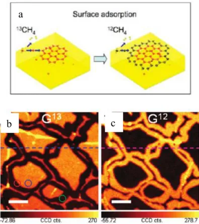
44However, people found the continues graphene film actually consists of many tiny merged grains, separated by GGBs. Afterwards, explosive studies have been devoted in the growth of large single crystalline graphene grain on Cu without GGBs. The size of as-grown single grain graphene increased from only several micrometers in the beginning to millimeter, even centimeter, only in 4 years.
29, 45-50Cu has been proved to be much easier to obtain monolayer graphene compared with Ni, due to the
extremely low carbon solubility (7.4 at. ppm at 1020 ℃).
51-52The speculation that the graphene gown over
Cu surface is mainly a surface process and is proved by using carbon isotopes (
13C and
12C) supplied
alternatively during the growth.
41Figure 2.9 illustrates the proposed model of graphene grown on Cu foil
and a designed experiment using isotopic labeling of the carbon processor (
13CH
4and
12CH
4were
introduced sequentially) can support the model very well. Figure 2.9b, c shows the Raman mapping of G
band of
13C and
12C. There are sharp boundaries between the
13C and
12C, indicating that there is no dissolved
carbon being included in the growth of graphene. This is the main distinction with Cu, on which such
boundaries cannot be found. Cooling rate here will not give impact on the layer numbers of graphene.
22
Figure 2.9 (a) Schematically presented graphene growth mechanism on a Cu substrate based on the surface deposition using a carbon isotope analysis. (b)
13G band (1500–1560 cm
−1) and (c)
12G band (1560–1620 cm
−1), which confirmed the model proposed in (a). Scale bars are 5 µm.
412.3.5. Large graphene grains grown on Cu by CVD
As introduced before, the CVD growth of graphene on Cu has become the most promising approach to obtain large area monolayer graphene but people found that the fully covered large-area graphene films grown on Cu foil usually contain a large number of GGBs.
53-54These grain boundaries were revealed to be coming from the stitching of various small graphene grains but have different crystal orientations with nearby.
55It may originate from that the graphene grains nucleate randomly on the catalyst surface without control. Figure 2.10a shows the mapping of GGBs with different high rotated orientation angles, which can be from 0 to 30° (Figure 2.10b). More information can be seen from Figure 2.10c that two sets of hexagonal
a
b c
23 diffraction patterns from two individual grains. The zoomed image in d shows the clear grain boundary between two grains, which is composed of carbon pentagons and heptagons mixed with hexagons. Such GGBs have been proved to have detrimental effects on both of the electronic and mechanical properties of graphene.
53, 56-58Figure 2.10 (a) Mapping of graphene GGBs overlapped with the graphene STEM image. The numbers indicate the misorientation angles. The scale bar is 2 µm. (c) Statistics of disorientation angles between adjacent grains. (c) High resolution STEM images of GGBs. The insert shows the Fourier transform of the image. The scale bar is 2 nm. (d) is the enlarged STEM image of the part of the red dashed rectangle in (c).
The scale bar is 0.5 nm.
55a c
b d
24
In order to observe the formed GGBs on Cu in large scale and more efficiently, serval approaches were
explored. Optical microscope can be used to observe the GGBs directly on Cu by selective oxidation of the
underlying Cu though GGBs (see Figure 2.11a,b). The oxidized Cu foil beneath the defective GGBs, allows
the visualization of GGBs without transfer.
59After transfer the as-grown graphene on glass, nematic liquid
crystals were coated on the graphene. Since the relationship between the orientation of the liquid crystals
and the underlying graphene, GGBs can be visible by using the polarized optical microscope (POM).
60Due
to the defects and higher chemical reactivity of GGBs, Kim, K. et al found that Pt nanoparticles can
predominantly deposit along GGBs by atomic layer deposition (ALD), after transfer to glass.
61Recently,
the direction of MoS
2grown on the top of graphene was found to depend on the orientation of underlying
graphene below, which was also applied to visualize the GGBs.
5725
Figure 2.11 Direct observation of GGBs on Cu foil. (a) Optical image of Cu foil after ultraviolet exposure under moisture-rich ambient conditions. (b) is the AFM image of the marked position in (a).
59(c) POM image of graphene on Cu foil after liquid crystal coating. (d) is the schematic illustration of liquid crystal molecules on polycrystalline graphene.
60(e) Schematic of selective Pt deposition on the defects of graphene.
SEM image of transferred graphene on glass then after (f) 500 and (g) 1000 ALD cycles of Pd deposition.
61Scar bars are 2 µm.
a
b
c
d
e
f g
26
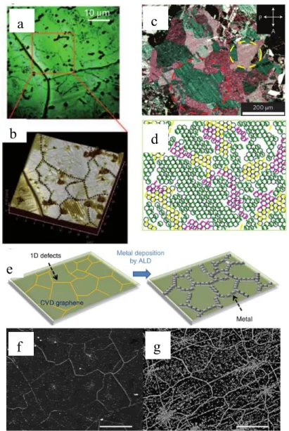
In order to achieve GGBs-free graphene, the synthesis of large graphene grain has become a hot topic and several methods have been proposed during the last five years.
The first approach is to decrease the nucleation density of graphene on Cu foil as low as possible. Lower
nucleation density means the number of graphene grains per unit area becomes smaller, providing a higher
possibility to get larger isolated single-crystal graphene grain. Graphene was found to prefer to nucleate at
the surface roughness,
62grain boundaries,
63and impurities
64on Cu foil. Therefore, using polishing to flat
Cu surface, thicker Cu foil to increase Cu grains
65and longer time H
2annealing,
46higher pressure
annealing
47, CO
2annealing
66of Cu surfaces to remove the impurities have been studied to reduce the
nucleation density, leading to the achievement of millimeter sized graphene grains. Making confined space
of Cu foil, such as Cu pocket,
67a vapor trapping method by putting Cu into a quartz tube with one head
closed,
68or sandwiched by quartz plates,
69-70was also demonstrated the success to reduce of nucleation
density. In 2013, Hao,Y. et al. found the introduction of oxygen gas during Cu annealing stage results in a
dramatic decrease of graphene nucleation density and the grain as large as centimeter isolated grain was
obtained (Figure 2.12a,b).
30Similar work was reported nearly at the same time that by only Ar annealing
with H
2excluded, as large as 6 mm hexagonal graphene grain was obtained successfully (Figure 2.12c).
71After that, many researchers focused on studying the influence of oxygen on graphene growth, many works
were got published.
72-77Seeking the mechanism behind is also very interesting and several different
mechanisms were proposed,
78such as Cu
xO passivation effect
71and carbon impurities removal.
79-81However, it is still unclear how oxygen contributes to the reduction of the nucleation density.
27 Figure 2.12 Large single graphene grains grown on Cu foil by the assistance of oxygen. (a) Relationship of graphene nucleation density and oxygen exposure time. (b) Photograph of 1 centimeter graphene grain on Cu foil.
30(c) Around 6 mm graphene grain after transfer on SiO
2/Si substrate.
71The second feasible way is the controlling of the orientation of graphene grains. Previous report revealed that all the graphene grains grown on Cu(111) were found to have the consistent orientation, while there is 30° rotated degree of graphene grains synthesized on Cu(100) (see Figure 2.13a-c).
82Graphene grains with the same orientation was proved to have seamless stitching between the grains (see Figure 2.13e).
83This method has no requirement on the nucleation density of graphene, however, high quality of single crystalline Cu(111) is needed as graphene grains were not aligned at the same direction on Cu(111) with rough surface.
83a b c
28
Figure 2.13 DF low energy electron microscope (LEEM) images of graphene grown on (a) Cu(111) and (b,c) Cu(100) films. The top insets are the LEED patterns. There are 30° rotated angles between b and c.
82Optical images of graphene grains merged with 15° mismatched angle (d, left) and 0°(e, left). The right panels of d and e are the optical images of graphene taken after UV-light irradiation for 20 min with 20%
humidity.
83a b
d
e
c
29 The third available way is making graphene nucleation sites controllable. If we can control the graphene grains to nucleate at the preferred positions, the formation of GGBs can be effectively solved. However, the triggers of graphene nucleation on Cu foil are very complicated, as graphene grains have been found to prefer to nucleate at defects and impurities,
64, 84as mentioned earlier. These impurities can be but is not limited to SiO
2particles,
84Cu oxide particle
85and carbon.
86The crystal orientation and morphology of Cu and CVD pressure were also proved to have great impacts on the graphene nucleation sites.
62-63, 87-88W. Wu et al. found that by deposing PMMA seeds arrays on Cu foil, graphene grains can selectively nucleate at the PMMA seeds (see Figure 2.14a,b).
89Graphene prefers to nucleate at the PMMA dots due to the high carbon concentration of PMMA. However, the size of controllable graphene was only limited to 10 µm as graphene will nucleate at other places if increase the interval of PMMA seeds. Moreover, very strong defect was detected at each nucleation center (Figure 2.14c). Recently, W. Tianru et al. proposed a
“locating feeding system” to grow a graphene grain at the desired positions on Cu-Ni alloy (Figure 2.14d).
90Thanks to the successful control of only one graphene grain at a pre-designed position of the substrate,
leads to the achievement of inch sized graphene grain (Figure 2.14e). However, this method was
demonstrated to be invalid on Cu foil, limiting the application.
30
Figure 2.14 (a) Schematic of position controlled graphene grains by PMMA seeds. SEM images of (b) graphene arrays after CVD from the patterned PMMA seeds. (c) Raman mapping of D band intensity of a graphene grain.
89(d) Schematic of strategy of the local feeding system in CVD. Optical image of graphene grains grown on Cu-Ni alloy (e) by local feeding method and (f) with a conventional CVD process.
902.3.6. Basic principle of CVD process
91CVD is one of the effective way for depositing thin films, which can be also fabricated by evaporation, sputtering, electroplating, etc. The advantage of CVD method in the film deposition is the superior conformity and large area availability, although the cost of CVD is not the lowest. One typical CVD system is mainly composed of quartz tube with good leakproofness, gas flow controllers which inject the precursor of deposition to the chamber accurately by the set value, a temperature controller that can precisely control the temperature, and a vacuum pump that can eject the residual gas or air remaining inside the tube or provides a low-pressure reaction environment.
a
b c
d e f
31 We often use “sccm” for the gas measurement. “sccm” is a volume unit which means “standard cubic centimeters per minute”. The standard conditions here are 1 standard atmosphere pressure and 0 ℃.
According to the ideal gas law: PV=nRT, P is the pressure, V the volume, n the number of moles, R the universal gas constant (~8.314 J mol
-1K
-1) and T the absolute temperature. Then I can calculate that 1 sccm contains ~7.4×10
-7moles per second. As the actual operation condition of CVD in ambient is close to the standard condition, the value still can be used by ignoring the thermal expansion.
The velocities of molecules in an ideal gas obey a Maxwell distribution and the mean velocity is:
𝐶 𝑚𝑒𝑎𝑛 = √ 8𝑘𝑇
𝜋𝑚 (2.10)
Bear in mind that the direction of the velocity is random, thus I can assume half of gas molecules will not heat the wall of tube: nC
mean/2. For the gas molecules strike to the wall can also be divided into the direct movement and perpendicular to the wall. Therefore, I can describe the flux of molecules to the wall as:
𝐽 = 𝑛𝐶
𝑚𝑒𝑎𝑛4 = 3.51 × 10 22 𝑃
√𝑀𝑇 (2.11)
where n is N/V, V is the volume and N is the molecules. The unit of J is in mole cm
-2sec, P in Torr and M in g mole
-1.
The mean free path (λ) is the average distance traveled by a moving particle without striking, which plays an important role in the determination of how fast transport mass, energy and momentum happen in the gas.
It can be calculated by:
λ = 1
√2𝜋𝑎
2𝑛 (2.12) where πa
2is the cross-section area.
The flux can be converted to an equivalent “deposition rate”:
𝑅[A/min] = 𝐾
𝑠1.7×10
−10𝜌
𝑚[𝑝𝑟𝑒] 𝑐ℎ (2.13)
32
where Ks is the rate constant (=exp(-E
a/RT), cm s
-1), [pre]
chis the species concentration, 𝜌
𝑚is the molar density of the deposited film.
Next let’s have an investigation of the CVD reactor. To simplify, here all gas concentrations are taken to be constant at all locations in the reactor, corresponding parameters are shown in Figure 2.15. According to the law of conservation of mass:
F in [pre] in =K s S[pre] ch +F in [pre] ch (2.14)
[𝑝𝑟𝑒] 𝑐ℎ = 𝐹
𝑖𝑛[𝑝𝑟𝑒]
𝑖𝑛𝐹
𝑖𝑛+𝐾
𝑠𝑆 (2.15)
The time of a gas molecule stays in the chamber are be expressed as residence time t res : 𝑡 𝑟𝑒𝑠 = 𝑉
𝐹
𝑖𝑛(2.16)
The consumption file time t con shows the average time of a molecule survived before reacted with the substrate:
𝑡 𝑐𝑜𝑛 = 𝑉
𝐾
𝑠𝑆 (2.17) Therefore, formula 2.15 can be rewritten as
[𝑝𝑟𝑒] 𝑐ℎ = [𝑝𝑟𝑒]
𝑖𝑛1+𝑡
𝑟𝑒𝑠/𝑡
𝑐𝑜𝑛(2.18)
Figure 2.15 CVD reactor and terminology.
9133 In the case of very low surface reaction ( t res << t con ), according to 2.18, [pre] ch ≈[pre] in . Thus the deposition reaction is only limited by the rate of the surface reaction.
On the other hand, very fast surface reaction ( t res >> t con ) , eq. 2.18 can be rewritten as:
[𝑝𝑟𝑒] 𝑐ℎ = [𝑝𝑟𝑒] 𝑖𝑛 𝑡
𝑐𝑜𝑛𝑡
𝑟𝑒𝑠(2.19)
This means the rate determined by the supply of reactant to the surface, which is transport limitation. In this case, the rate of surface reaction can be:
𝑅 = 𝐾 𝑠 [𝑝𝑟𝑒] 𝑖𝑛 𝑡
𝑐𝑜𝑛𝑡
𝑟𝑒𝑠= [𝑝𝑟𝑒] 𝑖𝑛 𝐹
𝑖𝑛𝑆 (2.20)
Thus it can be seen that the reaction rate is independent of temperature but relies on the inlet flow rate.
For a typical CVD condition of graphene growth on Cu foil in this thesis, the volume of graphene heating zone (V) is π× 2
2×30=376.8 cm
3. The input volume flow is 300 sccm=5 cm
3s
-1at 760 Torr. The temperature is 1075 ℃=1348 K. Thus the volume expand to 5× (1348/273) =24.7 cm
3s
-1. Therefore, the residence time can be estimated to t res =V/F in =376.8/24.7=15.2 seconds. In this thesis, CH
4is used as a carbon source and the typical mole fraction is 15 ppm (seen as an ideal gas).
The surface area S can be estimated by the area of quartz holder, where Cu foil is put on. The length is 5 cm and worth is 3.5 cm. Thus S is 17.5 cm
2and [pre]
in=4.5×10
-5moles/cm
3×760× (273/1348) ×15×10
-6