Japan Advanced Institute of Science and Technology
JAIST Repository
https://dspace.jaist.ac.jp/Title
Large anomalous Hall resistance of pair δ-doped
GaAs structures grown by molecular-beam epitaxy
Author(s)
Jung, D. W.; Noh, J. P.; Touhidul Islam, A. Z.
M.; Otsuka, N.
Citation
Journal of Applied Physics, 103(4):
043703-1-043703-8
Issue Date
2008-02-19
Type
Journal Article
Text version
publisher
URL
http://hdl.handle.net/10119/8539
Rights
Copyright 2008 American Institute of Physics.
This article may be downloaded for personal use
only. Any other use requires prior permission of
the author and the American Institute of Physics.
The following article appeared in D. W. Jung, J.
P. Noh, A. Z. M. Touhidul Islam, N. Otsuka,
Journal of Applied Physics, 103(4), 043703 (2008)
and may be found at
http://link.aip.org/link/?JAPIAU/103/043703/1
Large anomalous Hall resistance of pair
␦
-doped GaAs structures grown
by molecular-beam epitaxy
D. W. Jung,1J. P. Noh,1A. Z. M. Touhidul Islam,1and N. Otsuka1,a兲 1
School of Materials Science, Japan Advanced Institute of Science and Technology, Asahidai 1-1, Nomishi, Ishikawa 923-1292, Japan
共Received 2 October 2007; accepted 2 December 2007; published online 19 February 2008兲 Beryllium/silicon pair␦-doped GaAs structures grown by molecular-beam epitaxy exhibit a Hall resistance which has a nonlinear dependence on the applied magnetic field and which is strongly correlated to the negative magnetoresistance observed under the applied magnetic field parallel to the ␦-doped layers. Dependence of the occurrence of the nonlinear Hall resistance on the growth condition is investigated. A significantly large increase in both the magnitude and the nonlinearity of the Hall resistance is observed from samples whose GaAs buffer layers are grown under the condition of a low As/Ga flux ratio. Reflection high energy electron diffraction and electron microscope observations show that a faceted surface develops with the growth and postgrowth annealing of a GaAs buffer layer under the condition of a low As flux. From samples which have only Si ␦-doped layers and exhibit the n-type conduction, such nonlinear Hall resistance is not observed. The nonlinearity of the Hall resistance of Be/Si pair␦-doped structures depends on the single parameter B/T, where B and T are the applied magnetic field and the temperature, respectively. Based on these results, it is suggested that the nonlinear Hall resistance of Be/Si pair ␦-doped structures is the anomalous Hall effect caused by localized spins in␦-doped layers. © 2008
American Institute of Physics.关DOI:10.1063/1.2838487兴
I. INTRODUCTION
In recent years, active research aimed at incorporating the spin degree of freedom into semiconductor electronics has been carried out in the field called spintronics. Two ap-proaches have mainly been employed in the research. One approach is the incorporation of magnetic elements into semiconductor crystals as solute atoms, resulting in the for-mation of diluted magnetic semiconductors. Their represen-tative is Ga1−xMnxAs.1 The other approach is the effective
manipulation of spin-orbit interactions for the generation of spin-polarized carriers. Experimental results obtained in this approach which widely attracted attention are observations of spin Hall effects.2
There are various methods for engineering electronic structures of semiconductors due to the past significant de-velopment of fabrication techniques of semiconductor mate-rial structures, such as the growth of low-dimensional struc-tures. By utilizing these techniques, different approaches can be used for incorporating the spin degree of freedom into semiconductors. In a recent study,3we observed a Hall resis-tance which has a nonlinear dependence on the applied mag-netic field from Be/Si pair ␦-doped GaAs structures grown by molecular-beam epitaxy 共MBE兲. In the pair ␦-doped GaAs structures which exhibit p-type conduction, a metal-insulator transition occurs as a result of the strong localiza-tion of holes in the ␦-doped layers.4With the applied mag-netic field whose direction is parallel to the current, negative magnetoresistance was observed from these structures in the temperature range where the nonlinear Hall resistance
occurs.3,5Because of the strong correlation of the occurrence of the negative magnetoresistance and the nonlinear Hall re-sistance, the observed Hall resistance was explained as an anomalous Hall effect 共AHE兲 by assuming the existence of localized spins in the structures. The possibility of the exis-tence of localized spins in the pair ␦-doped structures was suggested from their similarity to localized spins associated with impurity states in bulk semiconductors such as P doped Si.6This hypothesis can be verified by using a method such as the measurement of the temperature dependence of the magnetization of a sample, but the small number of impurity atoms doped in␦-doped layers in one sample makes the use of such a method extremely difficult.
In our research, instead of using the method mentioned above, we investigated the dependence of the occurrence of the nonlinear Hall resistance on the growth condition in or-der to gain insights into its origin. We observed a signifi-cantly large increase in both the magnitude and the nonlin-earity of the Hall resistance from samples whose buffer layers were grown under the condition of a low As/Ga flux ratio. Reflection high energy electron diffraction 共RHEED兲 and electron microscope observations showed that a faceted surface develops with the growth and postgrowth annealing of a GaAs buffer layer under the condition of a low As flux. From samples which have only one Si ␦-doped layer and which exhibit n-type conduction, such an increase was not observed. The nonlinearity of the Hall resistance of Be/Si pair␦-doped structures depends on the single parameter B/T, where B and T are the applied magnetic field and the tem-perature, respectively. On the basis of these results, the pos-sibility of an AHE in the pair␦-doped structure is discussed. a兲Author to whom correspondence should be addressed. Tel.:
81-761-51-1500. FAX: 81-761-1149. Electronic mail: [email protected].
II. EXPERIMENTAL
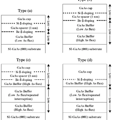
Figure1 shows four types of sample structures共a兲, 共b兲, 共c兲, and 共d兲 which were used in the present study. In the first three types of structures, a pair of Be and Si␦-doped layers with a 1 nm thick GaAs spacer were grown on a GaAs buffer layer after the buffer layer surface was annealed for 5 min under the As flux. The buffer layers were grown at 580 ° C, while the pair of␦-doped layers and a cap layer were grown at 530 ° C. A lower temperature for the latter was used in order to minimize Be diffusion from the␦-doped layer. The Ga flux was set at a constant value of 5.8⫻10−7Torr for all samples. The As flux and the thickness of the buffer layer varied among the samples. Table I shows the As flux, the buffer layer thickness, the doping concentrations of Be and Si, and the Hall coefficient RH at room temperature for 13
samples.
For the first six samples labeled 1–6, whose structures are of type 共a兲, the As flux varied among the samples, whereas all other growth conditions were identical. Sample 7 also has a structure of type 共a兲, but its Be and Si doping concentrations are lower than those of samples 1–6. The next three samples, 8–10, have the structure共b兲 whose first buffer layer was grown under a high As flux, at 2.5⫻10−5Torr, and whose second buffer layer was grown under a low As flux, at 0.98⫻10−5Torr, with different thicknesses ranging from 720 to 1800 nm. For sample 11, which is of type 共c兲, after the growth of the second buffer layer under the low As flux, the As flux was increased to a high value of 2.7 ⫻10−5Torr, and a 120 nm thick third buffer layer and a pair of ␦-doped layers were grown. During the growth of the second buffer layer, repeated growth interruptions with a du-ration of 5 min were made. The reason for the growth of this structure will be explained in the next section. Samples 12
and 13 have a structure of type共d兲, which was grown under conditions similar to those for type 共c兲, but have only a Si ␦-doped layer. These two samples exhibit n-type conduction, while all other samples exhibit p-type conduction.
The surface morphology of these samples was analyzed by RHEED, cross-sectional transmission electron micros-copy 共TEM兲, and scanning electron microscopy 共SEM兲. A square 5⫻5 mm2sample was cut for the van der Pauw mea-surements of sheet resistance and for Hall-effect measure-ments, and indium contacts were made at the corners of a square sample.4 The magnetic field used for the Hall-effect measurements has a value of 0.32 T. A rectangular 3 ⫻8 mm2 sample was cut, and four indium contacts with an equal spacing in the longitudinal direction and two indium contacts in the transverse direction were made for Hall resis-tance measurements.
III. RESULTS
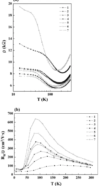
In the initial stage of the experiment, we changed the doping concentrations of Be and Si and the growth tempera-tures by maintaining flux conditions at normally used values for the growth of GaAs layers. Neither the magnitude nor the nonlinearity of the Hall resistance of the samples was found to increase significantly with these changes. In the following stage, we changed the As flux and found a significant change in the Hall resistance of the samples. Figure2共a兲shows plots of the sheet resistanceof samples 1–7 as a function of the temperature T. For all samples, the temperature dependence of exhibits a minimum. From the minimum, first in-creases rapidly with the decrease of the temperature, and its increase becomes smaller as the temperature decreases fur-ther.
Figure2共b兲 shows plots of RH/ as a function of T for
samples 1–7, where RH is the Hall coefficient. If only the
normal Hall effect occurs, RH/corresponds to the Hall
mo-bility. For all samples, RH/ increases with the decrease of
the temperature from 300 K, reaches a maximum, and rap-idly decreases with further lowering of the temperature. In the low temperature range below 30 K, RH/ becomes
nearly constant. There is a direct correlation of the tempera-ture dependence of RH/ with the As flux for the growth of
GaAs buffer layers in these samples. As the As flux de-creases from 2.61⫻10−5Torr, the maximum value of R
H/
gradually increases, reaches the highest value at 0.98 ⫻10−5 Torr, and decreases with a further decrease of the As flux to 0.77⫻10−5Torr. The buffer layer of sample 7 was grown with an As flux of 0.98⫻10−5Torr, similar to that of sample 5, but its Be and Si concentrations are lower than those in sample 5, at 4.7⫻1012and 1.8⫻1011cm−2, respec-tively. As seen from the results for samples 5 and 7 in Fig.
2共b兲, lower Be and Si concentrations led to higher values of
RH/ for the same growth condition for the buffer layers. The Si concentration in sample 7 was lowered significantly from that in samples 2–6, becoming nearly one quarter of the latter, in order to obtain a resistivity that is comparable to that of the latter samples; if the Be and Si concentrations were lowered by keeping the same ratio of the concentra-tions, the resistivity of a sample was found to increase sig-FIG. 1. Layer configurations of the Be and Si pair␦-doped structures of
types共a兲, 共b兲, 共c兲, and 共d兲.
nificantly and to exhibit an insulatorlike temperature depen-dence over the whole temperature range. Because higher values of RH/ can be obtained, Be and Si concentrations
similar to those in sample 7 were doped in the remaining pair ␦-doped samples 8–11.
Figure3共a兲shows the Hall resistance RHallof sample 5 as a function of the applied magnetic field B. Hall resistance curves were obtained by calculating 关RHall共B兲−RHall共–B兲兴/2 with the measured values of RHall共B兲 and RHall共−B兲 for each value of the magnetic field B in order to remove contribu-tions of the magnetoresistance to the Hall resistance. The figure shows a highly nonlinear dependence of RHall with respect to B. The nonlinearity increases with the lowering of the temperature, but below 30 K, RHall is completely linear with B. The nonlinearity of the Hall voltage for sample 5 is significantly greater than that for other samples grown under higher As fluxes.3 Figure3共b兲 shows the longitudinal resis-tance of sample 5 as a function of the applied magnetic field
B. The magnetic field was applied in the direction parallel to
the current. As seen in the figure, the longitudinal resistance initially increases with B and starts to decrease at higher values of B, corresponding to a negative magnetoresistance. The As flux used for the growth of sample 1 is the nor-mal value for the MBE growth of GaAs layers. A bright共2 ⫻4兲 RHEED pattern typical to the As-rich 共001兲GaAs sur-FIG. 2.共a兲 Temperature dependence of the resistivityand共b兲 temperature
dependence of the Hall coefficient RH/for samples 1–7.
FIG. 3. 共a兲 Hall resistance RHallof sample 5 as a function of the magnetic
field B and共b兲 magnetoresistance of sample 5 as a function of the magnetic field B applied in the direction macroscopically parallel to the current.
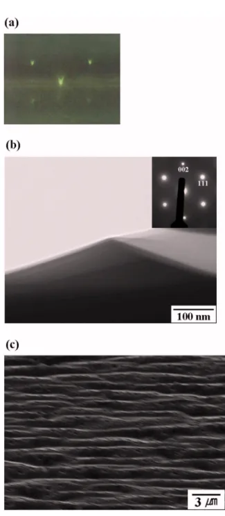
face was observed during the growth of the GaAs buffer layer in this sample. In the case of the six other samples 共2–7兲 with lower As fluxes, RHEED patterns gradually be-came darker during the growth of the GaAs buffer layers, indicating a roughening of their surfaces. With the 5 min annealing following the growth of the buffer layers, RHEED patterns became brighter and exhibited V-shaped spots in the 关1¯10兴 direction of the incident electron beam, as shown in Fig. 4共a兲. As the As flux was set to a lower value, more distinct V-shaped spots were observed. The appearance of these V-shaped spots indicates the formation of a faceted structure of the 共001兲GaAs surface due to the annealing process.7 The faceted structure can be directly seen in a
cross-sectional TEM image, as shown in Fig.4共b兲, and was observed for sample 4. In the TEM image, the lower dark area is the cross section of the sample near its surface, and the small darker area on the right-hand side is a remaining epoxy film which was used for the preparation of a cross-sectional sample. The TEM image shows the formation of a well-defined faceted structure. Facet planes were identified as 共114兲 and 共1¯1¯4兲 planes with TEM images and RHEED patterns.
The results presented above suggest a direct correlation between the formation of a faceted surface and the large increase in the magnitude and nonlinearity of the Hall resis-tance. We therefore next tried to grow samples which had highly developed faceted surfaces. For this purpose, we ini-tially grew a buffer layer with an atomically flat surface by using a high As flux, and then grew a thick buffer layer with a low As flux, as shown by the type 共b兲 structure in Fig.1. Samples 8–10 were grown in this way. For sample 11, re-peated growth interruptions were made during the growth of the second buffer layer in order to develop a faceted surface. Figure 4共c兲 is a SEM image of the surface of sample 11 which shows highly developed faceted surfaces. Figure5共a兲 shows plots of RH/ as a function of T for samples 8–11.
The figure shows that RH/ significantly increases as the
thickness of the second buffer layer increases. At room tem-perature, all samples have nearly identical values of RH/,
but RH/ rapidly increases with a decrease in the
tempera-ture and reaches a maximum around 50 K. Below 40 K,
RH/is sharply reduced to values around 50 cm2/V s for all
samples. Maximum values of RH/ for samples 10 and 11
are nearly identical, although a high As flux was used in the growth of ␦-doped layers and of a cap layer for the latter sample. Figure5共b兲shows the Hall resistance RHallof sample 8 as a function of the magnetic field B. Hall resistance curves for this sample are highly nonlinear as compared to those for sample 5.
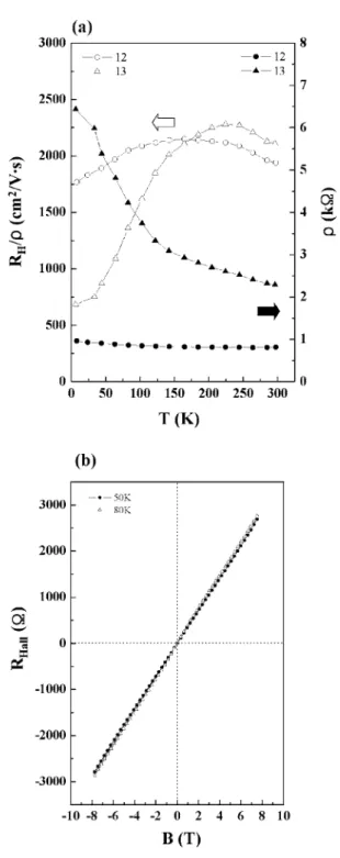
Figure 6共a兲 shows RH/ and for the n-type samples,
samples 12 and 13, as a function of the temperature T. The growth of the buffer layers in these samples was made in the same way as for sample 11. The Si doping concentrations in these two samples were selected so as to give rise to carrier concentrations that are comparable to those of the p-type samples. The figure shows no significant enhancement of
RH/values, unlike the case of the p-type samples. Values of
RH/for these samples are comparable to reported values of the Hall mobility of Si␦-doped GaAs samples.8 Figure6共b兲 shows RHallas a function of the magnetic field B for sample 13. No significant nonlinearity is observed in these RHall curves at both temperatures of 50 and 80 K.
IV. DISCUSSION
The present results show that the Hall resistance of a pair ␦-doped sample is significantly affected by the growth of a buffer layer grown under a low As flux condition. The most significant change is a very large increase of the value of
RH/. The highest values for samples 10 and 11 reach ap-proximately 8000 cm2/V s at around 50 K, as seen in Fig.
5共a兲. This value is much higher than the reported values of FIG. 4. 共Color online兲 共a兲 关1¯10兴 RHEED pattern for a GaAs buffer layer
grown under a low As flux condition at 0.98⫻10−5Torr and annealed for
5 min.共b兲 Cross-sectional TEM image of a faceted surface for sample 4 with a corresponding transmission electron diffraction pattern.共c兲 SEM im-age of the surface of sample 11.
the Hall mobility for Be␦-doped GaAs layers.8The highest reported value at 60 K is approximately 2000 cm2/V s, which was obtained with a Be concentration of 1 ⫻1012cm−2. For Be concentrations similar to those in samples 10 and 11, the reported Hall mobility at 60 K is less than 1000 cm2/V s.8
As explained earlier, all pair ␦-doped samples from 1 to 11 exhibit p-type conduction over the whole measured temperature range. For example, the Hall coefficient RHfor sample 11 has positive values 184, 1080,
and 4850⍀ T–1at 300, 100, and 50 K, respectively.
It is known that Ga droplets form in a GaAs layer grown under a low As flux condition,9and a semiconductor sample with such metallic inclusions exhibits an apparently high Hall mobility.10 Such a high Hall mobility has been ex-plained as the result of a large positive magnetoresistance caused by a geometrical effect at an interface between the
semiconductor matrix and metallic inclusions;10to calculate the Hall mobility, the resistivity at a zero magnetic field, which is lower than that obtained for the value of the mag-netic field used for the measurement of the Hall voltage, is normally used, resulting in an apparently high value of the mobility. All samples used in the present experiment exhibit positive magnetoresistance with the magnetic field direction perpendicular to the sample surface, but the increase in the resistance with the magnetic field used in the measurement of the Hall effect, B = 0.32 T, reaches only a few percent for these samples; the increase in their nominal Hall mobility due to this effect is expected to be only a few percent. Very FIG. 5. 共a兲 Plots of RH/as a function of the temperature T for samples
8–11.共b兲 Hall resistance RHallof sample 8 as a function of the magnetic field
B.
FIG. 6. 共a兲 Temperature dependence of the resistivityand of RH/for
samples 12 and 13.共b兲 Hall resistance of sample 13 as a function of the magnetic field B.
high values of RH/for samples 10 and 11, therefore, cannot
be attributed to the existence of Ga droplets. This conclusion is also supported by the results obtained for the Si␦-doped samples 12 and 13, which do not show any significant en-hancement of the Hall mobility. The RH/ value for sample
13, which corresponds to the Hall mobility, becomes lower than that for sample 12, although sample 13 has a lower Si concentration than sample 12. The resistivity of sample 13 also significantly increases as the temperature is lowered. These results suggest a tendency to carrier localization at low temperatures in this sample. Such carrier localization may have been induced by carrier trapping in the surrounding matrix of the␦-doped layer.
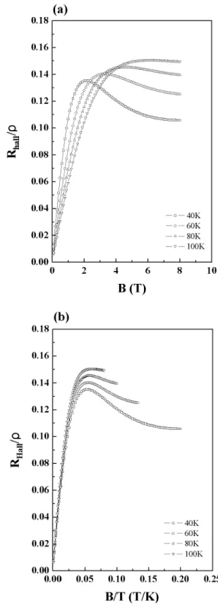
There is a distinctive dependence of the nonlinear part of Hall resistance curves of pair ␦-doped samples on the mag-netic field B and the temperature T. In Figs.7共a兲and 7共b兲, the quantity关RHall/共T兲−RHall/共20 K兲兴 is plotted as a func-tion of B/T for samples 6 and 8, respectively, where
RHall/共20 K兲 is the linear change of RHall/with B at 20 K. The division of RHall by is carried out in order to remove the effect of the magnetoresistance. These figures show that the nonlinearity of RHall/ depends on the single parameter
B/T. For both samples, whose RHall/ values are signifi-cantly different, the maxima and minima of the curves occur at nearly the same values of B/T. The Hall resistance curves for other samples show a similar dependence on B/T.
Very high values of RH/ and the dependence of the
nonlinearity of RHallcurves on the single parameter B/T sug-gest the possibility of an AHE caused by localized spins in a paramagnetic state in these pair ␦-doped structures, which we explain as follows: the anomalous Hall effect leads to the presence of an additional term in RH/, hence resulting in an
apparently high Hall mobility. The thermal average of the spin polarization induced by the magnetic field which results in AHE depends on the single parameter B/T. Negative mag-netoresistance observed in these pair␦-doped structures with a magnetic field parallel to the current also suggests the pos-sibility of the existence of localized spins in a paramagnetic state.3,5 In the case of ␦-doped layers grown on a faceted surface, positive magnetoresistance due to the normal com-ponent of the magnetic field occurs along with the negative magnetoresistance, resulting in the magnetoresistance curves shown in Fig.3共b兲.
By considering the possibility of the manifestation of an AHE, RHall/curves are calculated in order to reproduce the experimental results. For the calculation, we assume that the electrical conduction in these structures occurs through two paths: one path is produced by holes in the valence band, and the other by holes in an impurity band of the␦-doped layers. It is assumed that both paths contribute to the conduction at high temperatures, but below 30 K, only the latter path dominates the conduction. The conductivity of these two paths are denoted as1and2, respectively, with the mobil-ity of the former,1, being higher than that of the latter,2. The AHE term is added to the Hall coefficient for the con-duction in the valence band,
RH1=
1 1
冉
1+c具S典
B
冊
, 共1兲where c is a constant and具S典 is the thermal average of the spin polarization. Here, AHE is assumed to occur through the skew scattering which is known to be significant for high mobility carriers.11For the conduction in the impurity band with low carrier mobility, AHE is not considered. When con-sidering localized spins in a paramagnetic state, the average FIG. 7. Plots of关RHall/共T兲−RHall/共20 K兲兴 as a function of B/T for 共a兲
sample 5 and共b兲 sample 8.
spin polarization is given by the Brillouin function Bs共x兲,
具S典 = SBs共x兲, x = SgBB
kBT , 共2兲
where S and g are the spin and the Landé g factor, respec-tively. The dependence of the RHall/ of the system on B is given by RHall/= x1RH 11共1 + 2 2 B2兲 + x22关1 + 共RH 11兲2B2兴 1 +共x12+ x2RH 11兲2B2 B, 共3兲 where x1= 1 1+2, x2= 2 1+2. 共4兲
Without the AHE term, Eq. 共2兲becomes a standard formula of RHall/ for the system with two conduction paths.12
If the AHE term, that is, c具S典/B, is significantly larger than1 and2, Eq.共3兲 gives rise to Hall resistance curves, similar to the experimental curves, as shown in Fig. 8共a兲. Figure 8共b兲 shows that the nonlinearity of the calculated curves depends on the single parameters B/T. For the calcu-lation, it was assumed that 1= 300 cm2/V s, 2 = 50 cm2/V s, x
1= 0.2, and x2= 0.8. For the calculation of the Brillouin function, S and g were assumed to be equal to 21 and 2, respectively. The value of the constant c was chosen by assuming that c具S典/B=4000 cm2/V s at T=60 K for small values of B. A linear term which corresponds to2B is
not subtracted from RHall/in Fig.8共b兲because its contribu-tion is very small in this case. Besides具S典, the other param-eters 1, 2, x1, and x2 also change with the temperature, unlike the assumption made for the above calculation. Even with the inclusion of the temperature dependence of these parameters, RHall/ curves were found to depend approxi-mately on the single parameter B/T under the condition that the AHE term c具S典/B is far larger than1and that x2 does not change appreciably with the temperature. By fine tuning the temperature dependence of other parameters appropri-ately, calculated profiles of RHall/ which better reproduce experimental profiles can be obtained. The results of the cal-culation hence show that the large nonlinearity of the Hall resistance curves and the dependence on the single parameter
B/T result from two conduction paths with different values
of the hole mobility, where the contribution of the anomalous Hall term dominates the RHof the higher-mobility path.
Finally, we consider the question as to why the value of
RH/ significantly increases through the growth of a Be/Si
pair ␦-doped structure on a faceted surface. Experimental results relevant to this question are summarized as follows. The RH/value increases primarily through the development
of a large-scale faceted surface structure. Such a faceted sur-face structure develops through the growth of a thick GaAs buffer layer under a low As flux condition and through the postgrowth annealing of the surface. The growth of a pair of ␦-doped layers and of a cap layer under a low As flux con-dition is not responsible for the significant increase in the value of RH/since sample 11, which has a structure of type
共c兲, exhibits large values of RH/similar to those for sample
10. Lower concentrations of Be and Si for a pair of␦-doped layers also give rise to higher value of RH/, as seen from
the results for samples 5 and 7 in Fig. 2共b兲, although their effect is not as significant as that of the development of a large-scale faceted surface structure. Another experimental result which may be relevant to the above-mentioned ques-tion is that, in spite of large variaques-tions of values of RH/
among pair␦-doped samples, values of RH/for all samples FIG. 8. Calculated profiles of共a兲 RHall/as a function of B and共b兲 RHall/
become lower than 100 cm2/V s at temperatures below 40 K. This result suggests that the occurrence of the high value of RH/ is attributable to holes thermally excited to
high energy states.
The AHE results from the spin polarization of carriers which is induced by their interaction with localized spins.13 Therefore, in order to clarify the origin of the significant increase in the value of RH/, it is essential to understand
how the carrier transport process in the pair␦-doped struc-ture grown on a faceted surface changes from that in the pair ␦-doped structure grown on a共001兲 singular surface. Carrier transport properties of␦-doped semiconductors are known to be different from those of homogeneously doped semiconductors.8 The main difference results from the spreading of wave functions of high energy states from the ␦-doped layer into the surrounding matrix. The experimental results described above suggest that these high energy states and, hence, the carrier transport process through these states change significantly through the growth on a faceted surface. For example, the distribution of carrier trap sites in the sur-rounding matrix may have changed through the growth on a faceted surface. It is, however, difficult to clarify such changes with the present experimental results alone. In order to answer the question above, we need further analyses of the carrier transport process in ␦-doped structures grown on a faceted surface, including an analysis of Si␦-doped samples similar to samples 12 and 13.
To summarize, this paper presents the results of magne-totransport measurements of Be/Si pair␦-doped GaAs struc-tures whose buffer layers were grown under low As flux conditions. Two main results, significantly higher values of
RH/ than the reported values of the Hall mobility of Be ␦-doped GaAs layers, and the dependence of the nonlinearity of the Hall resistance curves on the single parameter B/T, are
reasonably explained by assuming the occurrence of an AHE caused by localized spins in the ␦-doped structures. Other results such as the negative magnetoresistance observed with the magnetic field parallel to the current and the lack of enhancement of the value of RH/ for Si ␦-doped samples
are consistent with this assumption. These results do not nec-essarily constitute direct evidence for the occurrence of an AHE or for the existence of localized spins in the pair ␦-doped structures, but they point the way to further re-searches aimed at investigating such possibilities.
1H. Ohno, A. Shen, F. Matsukura, A. Oiwam, A. Endo, S. Katsumoto, and
Y. Iye, Appl. Phys. Lett. 69, 363共1996兲.
2Y. Kato, R. C. Myers, A. C. Gossard, and D. D. Awaschalom, Science 306,
1910共2004兲; J. Wunderlich, B. Kasestner, J. Sinova, and T. Jungwirth, Phys. Rev. Lett. 94, 047204共2005兲.
3J. P. Noh, S. Iwasaki, D. W. Jung, A. Z. M. Touhidul Islam, and N. Otsuka,
Phys. Rev. B 75, 195307共2007兲.
4J. P. Noh, F. Shimogishi, and N. Otsuka, Phys. Rev. B 67, 075309共2003兲;
J. P. Noh, F. Shimogishi, Y. Idutsu, and N. Otsuka, ibid. 69, 045321 共2004兲.
5Y. Idutsu, J. P. Noh, F. Shimogishi, and N. Otsuka, Phys. Rev. B 73,
115306共2006兲.
6K. Andres, R. N. Bhatt, P. Goalwin, T. M. Rice, and R. E. Walstedt, Phys.
Rev. B 24, 244共1981兲; S. Ikehata, T. Ema, S. Kobayashi, and W. Sasaki, J. Phys. Soc. Jpn. 50, 3655共1981兲; M. A. Paalanen, J. E. Graebner, R. N. Bhatt, and S. Sachdev, Phys. Rev. Lett. 61, 597共1988兲.
7L. Däweritz and R. Hey, Surf. Sci. 236, 15共1990兲.
8E. F. Shubert, Semiconductors and Semimetals, Vol. 40共Academic,
Bos-ton, 1994兲, Chap. 1, p. 81.
9J. Osaka, N. Inoue, Y. Mada, K. Yamada, and K. Wada, J. Cryst. Growth
99, 120共1990兲.
10C. M. Wolfe and G. E. Stillman, Semiconductors and Semimetals, Vol. 10
共Academic, Boston, 1975兲, Chap. 3, p. 211.
11S. Onoda, N. Sugimoto, and N. Nagaosa, Phys. Rev. Lett. 97, 126602
共2006兲.
12R. A. Smith, Semiconductors, 2nd ed.共Cambridge University Press,
Cam-bridge, 1978兲, p. 114.
13J. Cumings, L. S. Moore, H. T. Chou, K. C. Ku, G. Xiang, S. A. Crooker,
N. Smarth, and D. Goldhaber-Gordon, Phys. Rev. Lett. 96, 196404共2006兲.