Electrical Properties of Evaporated Bismuth Thin Films (I)
journal or
publication title
福井大学工学部研究報告
volume 20
number 2
page range 123‑129
year 1972‑09
URL http://hdl.handle.net/10098/4729
~Ied:rical Properties of ~vaporated Bismuth Thin I=ilms (I)
Masasi INOUE* and Hisao Y AGI*
(Received Feb. 18, 1972)
The resistivity and magnetoresistance have been measured over the tem- perature range from 78 to 300 K for bismuth films (thickness range 100-- 2,000.1\) deposited on a glass substrate prepared by the vacuum evaporation technique at room temperature. Other experimental data such as coating and electrical contacts were also obtained to study the reproducibility of the films. The dependences of the resistivity on thickness and temperature are compared with other data reported to date about the scattering mechanism and size effect.
§ 1. Introduction
The bulk properties of bismuth crystals have so far been extensively studied about the Fermi surface from many experiments such as cyclotron resonance, de Haas-van Alphen effect, Shubnikov-de Haas effect, anomalous skin effect, magneto- acoustic, and thermo-magnetic effect, as well as magnetoresistance effect. About these aspects there are already review papers. 1-4)
On the other hand, there' are tremendous number of works on the bismuth films as well, from both the theoretical and experimental interest. Thin films are known to be different in physical properties from the bulk, because of crystalline structure (polycrystalline and amorphous) and dimensional size (size effect). For example, Buckel, et al.5) made it clear that Bi films deposited at 2 K appear to exist in phase different from those of the normal room temperature structure and the films show a phase transformation on annealing between 14 and 20 K, with the simultaneous change in the electrical resistivity. These amorphous films prepared at liquid helium temperature are found to be superconductive.S)
Furthermore, the resistivity, Hall effect, and magneto resistance measurements for the films (200-20,000 A) made at room temperature were also carried out over the temperature range from 77 to 300 K by Sawatari, et al.n to study the size effect and scattering mechanism of the electron and hole. They found that the thickness-dependence of the resistivity is mainly caused by the change in the mean free path and in the carrier concentration with thickness of the films, and that the negative temperature coefficient of the resistivity is due to the difference in the temperature dependence of the mobility between the bulk and the films. Recently Orgin, et al.8) reported that the mobility, Hall coefficient, and magneto resistance for
* Department of Applied Physics.
Bi films deposited on a mica depend on the thickness and oscillate with it. This phenomenon is known as the quantum size effect, although it is not well co nfirmed.9)
Our primary interest is not only concerned with Bi films themselves but also its application to such a magnetic field sensor. This preliminary experiment is one of our series of research. In this paper are described the similar measurements of the electrical properties of Bi films prepared at room temperature to confirm the current data. Measurements were also made of degradation of the films with exposure time in air. In a previous paper 1 0) we have already used polycrystalline small Bi wire as a magnetic field detector for a superconducting magnet.
§ 2. Experimental
Elemental Bi used, of four-nine purity and commercially available, were evaporated at pressures around 10-5 Torr onto a usual glass substrate at room temperature.
The substrate was cleaned by a solution of chromic acid mixture prior to evaporation.
A tungsten heater of 1 mm diameter was employed for evaporation, through which ae current was supplied in the range 15-20 A (evaporation speed 2-15 A/sec for Bi).
Two heater coils 'were prepared here, one wound helically for the electrodes and the other wound conically for Bi. The heater for Bi was at first kept above the sub- strate, but later it Was reversed because of homogeneity of the deposited films.
Although a variety of measuring methods for film thickness have been invented such as optical, ultrasonic, electrical, and X-ray technique, we have used the most simpliest one, weight method, as shown in Fig. 1. The thickness tx at a point x from the vertical position
°
is to a good approximation expressed bytx=to (1+ (x/h)2J -3/2, ···(1)
'where h is the distance between the source (heater) and the point 0, and to is the thickness at x = 0, given by to = m/4rrPh2•
O~X
(
~
Source
Fig.l Geometry of the weight method for thickness determination.
Here m is the evaporated Bi mass, and p the density (=9.747 g/cm3). Usually the height h was 12 em and maximum value of x Was within 9 em. A precision balance was used to measure the mass m within accuracy of 0.1 mg. The conventional de potentiometric method was used for the electrical measure- ments.
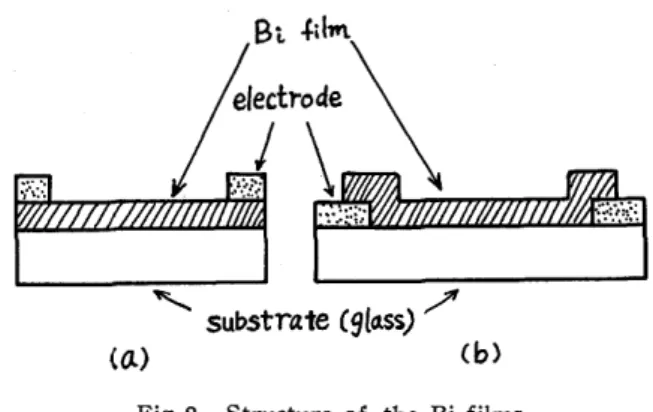
Sawatari, et al.n used In metal as an electrode. In addition to the metal, we further tried to use another metals (eu and Wood's metal) available on hand. These difference were compared by the value of the resistance between the two terminals, as shown in Fig. 2 (a), where the metals were
deposited after Bi evaporation under the same condition (vacuum, thickness, area of the substrate). The metal with lower resistance is considered to be good electrical contact.
Comparison of the resistances showed that Cu is a good electrode for the present experiment, and we have used thereafter Cu metal only and
Bi.
.fil1'l""
substrate (g{ClSS) /"<a)
(b)Fig.2 Structure of the Bi films.
the structure of the films used for measurement is shown in Fig. 2 (b).
§ 3. Experimental results 3-1. Stability of Bi films
The bulk Bi itself is stable in chemical nature, While evaporated Bi is to some extent not stable but rather active to the atmosphere. We measured the change in the resistance of the films with
time in air after deposition for two films of about 100 A. thickness and about 1,000
A.
Fig. 3 (a) shows the result for the thinner sample exposed in air, indicating a little change with the exposure time.For the thicker sample, the change is negligibly small, as shown in Fig. 3 (b), where comparison is made of the behavior between the samples with different coating material, two kinds of araldite and vacuum grease, but no diffe- rence is seen. Although thinner films were a little affected by air (oxidation and thus formation of Bi-oxides), we did not coat the surface of the Bi films any more, since the change was less than a few percent and at low temper- ature the coated films were easily broken mechanically due to the difference in the thermal expan-
2(0...--.---..---,.---,.---....---,
(o.)t""looA
2~OL-~-~2~~3~~4~~S~~6 Time (HORN)
(b) ;;::.1000A 21 ••
2J,2
Fig. 3 The change in the resistances of the Bi films with time, being exposed in air after evaporation, (a) for thickness ... l00
A and (b}-l,OOOA, with and without coating.
sion coefficient between Bi films and coating material.
3-2. Thickness-dependence of the resistivity
Fig. 4 shows the dependence of the resistivity at room temperature on thickness for the various films prepared by two different evaporation speed, one at 2-5 A/sec (heater current 15 A) and the other 10-15 A/sec (heater current 20 A), where the bulk resistivity (-1.1x10⁻⁴ ohm-em) is
also indicated for comparison. It is seen that the behavior is differ- ent between the samples with the different evaporation speed, and that the films deposited with high speed are less resistive than those with low speed. At first sight, the crystalline structure grown slowly may be imagined to be more closely packed and thus conductive than those grown rapidly. Although the situation is somewhat different, this trend is demonstrated by the Hall effect measurement on the Bi films made at liquid helium temperature that the films with the closer pac- ked phase have more carrier density and are more conductive than those with polycrystalline Bi on annealing at high temperature.S) But this is not the case for our results. Since the Hall coefficient has not yet been measured in this study we
300K
161~---~---~
~ eVllport1.tIOn speed 2-5 A/sec
--6-- q 10-15 p/sec
-~ 10r-r---~ -2
I
1
o1(?I--~---i
A
~~ __ A A.,,_~- - ... ll
A ' 6
~ ... -ll.-
Fig. 4 The thickness-dependence of the resisti- vity for Bi films prepared by two diffe- rent evaporation speed.
cannot draw a conclusive results, but it may be anticipated that these difference may possibly be due to 'crystalline structure, e. g., grain size and scattering mecha- nism (mean free path, carrier density, and mobility).
The thickness-dependence of the resistivity is seen different between the evaporation speed of the Bi films. The films deposited with high speed are quite similar to those reported by Sawatari, et al.1l i. e., the resistivity begins to increase at around 1,500-2,000 A with decreasing thickness, except the absolute value at higher thick- ness (ours;:::; 2 x 10⁻⁴ and theirs;:::; 4 x 10⁻⁴ ohm-em). On the other hand, for the films grown slowly its increase begins at-500
A
and the rise is very steep. These differences in the values of thickness are also considered as due to the several factors stated above. Furthermore, though not conclusive, the resistivity is likely to oscillate with thickness, as shown by the dotted lines in Fig. 4. This must, however,be confirmed by more detailed examination, as reported by Sawatari.9)
3-3. M agnetoresistance and temperature dependence of resistivity
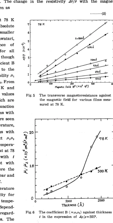
The transverse magnetoresistance of the films prepared rapidly (heater current 20 A) have been measured at 300 and 78 K, where the applied magnetic field is perpen- dicular to the film surface. The change in the resistivity dP/P with the magnetic field H is in general written as
dP/P = BH2.
Fig. 5 shows the results at 78 K for various films. The absolute values of dP/P are a little smaller than those observed by Sawatari, et al.7) The H2-dependence of dP/P is we'll established for all samples and even at 300 K, though not shown here. The coefficient B in Eq. (2) is roughly equal to the product of the electron mobility III
and hole mobility 1l2; B= 1l11l2. From the slopes in Fig. 5 at 78 K and those at 300 K, we get the values B in unit of mobility, which are demonstrated in Fig. 6 as a function of thickness t. For the films with t <1,400 A ,the values B are seen less dependent on temperature, while for the thicker films with
t>
1,400 A the product 1l11l2increases with lowering tempera- ture. It is further noted that at 78 K it increases sharply with t above 1,400 A, in contrast with the results at 300 K, where the product shows rather a linear and monotonic dependence on t.
Fig. 7 shoW's the temperature dependence of the resistivity for the same samples over the tempe- rature range 78-300 K. The depend- ences are nearly the same regard- less of the film thickness. The resistivities increase gradually
··· .. (2)
7 78 K
6 5
2
A 4~A
~
q50A 350A • .°O~~~~~'00~~~~~*O~~~~;~OO~~~~~
M~eti.c Field. H2 (1!106 4~)
Fig. 5 The transverse magnetoresistance against the magnetic field for various films mea- sured at 78 K.
°OL-~~--L-~~--~~-J--~2~0700~~
1000 0 Thickness (A)
Fig. 6 The coefficient B (=f.llf.l2) against thickness t in the expression of .dp/p=BH2.
with lowering temperature, while the bulk Bi is known to have positive temperature coefficient. 11)
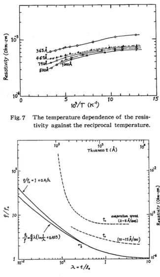
§ 4. Qualitative discussion Since in the present study the Hall effect is not measured and thus there is no information about the carrier concentration, we can- not discuss the detailed scattering mechanism involved. But we may be able to discuss the above results qualitatively as follo'Ws.
First, let us consider the thick- ness dependence of the resisti- vity observed at room tempera- ture, the size effect. This effect is usually considered as due to the change in the mean free path of the carriers, compared with the bulk. Many attempts have been made of the theoretical calcula- tiony,12) The ratio of the resis- tivity P of a film 'With thickness t to that of the bulk Po is expressed by 12>
P/Po=I+0.4/ A'" ···(3), or Po/p =
!
A[ln(~
) +0.423]. ···(4)Fig. 7 The temperature dependence of the resis- tivity against the reciprocal temperature.
101 105 •
T"ickness t (A)
...
.... , ... - t.
... _,-... (1o-1SA!sec)
--...---
Fig 8 The log-log plots of Fig.4 against t and the calculated curve12) against A =t/lo•
where A is the ratio of the thickness t to the bulk mean free path 10 ; A=t/lo• The calculated values are plotted in Fig. 8 against A, where are also given the observed resistivity for two kinds of films (heater current 15 and 20 A) from Fig. 4, simply for qualitative comparison. The behavior of the films prepared rapidly is in qualitative agreem,ent with the calculated curve, while for the films prepared slowly a discrepancy is seen to be large. This may be due to the fact that the surface of the films with t <200 A may easily be oxidized by air to become high resistive Bi-oxides, as mentioned previously.
The temperature dependence of the resistivity, as shown in Fig. 7, is qualitatively understood by using a usual transport theory for two carriers.11l The conductivity do
for the two bands, one for electron 1 and the other for hole 2, is written by
···(5)
where 1Zi, Ti, and mi (i=1,2) are the number of carriers, time of relaxation, and effective mass, respectively. The magnetoresistance is expressed by, for nl~n2=n as in bulk Bi,
P-Po = do-d = (~)2 ~ dOl d02 =
Po d ec n2 Pi = e'ri ... '(6)
mi' where Pi is the mobility. The resistivity is
Po = _1_ = 1
do n-e(P1
+
P2)" ···(7)The temperature dependence of Po is, therefore, due to the change in the number of carriers n and mobility Pi. The magnetoresistance data for the films with t
<1,400 A show PIP2 to be less dependent on temperature. In this case, the negative temperature coefficient of Po is supposed to be due to the decrease in n.
Since we have no data about n, the detailed discussion may be impossible at present, which will be reported later.
Acknowledgement
We thank S. Ito for the measurements and discussion. Thanks are due to our colleagues for technical assistance. One of us (M. I.) would like to express his sincere thanks to Professor E. Tatsumoto (Hiroshima University) for many useful advice. A part of this study has been supported by the Scientific Research Funds from the Ministry of Education.
References
1) S. Mase: Physical Properties of Metals, ed. by J. Yamashita and T. Suzuki (Shokabo, Tokyo, 1968) Chap. 2, p. 59. [in Japanese].
2) S. Tanuma: Physics of Low Temperature, ed. by T. Sugawara, S. Tanuma, and K. Yasukochi (Asakura-shoten, Tokyo, 1969) Chap. 5, p. 119. (in Japanese].
3) W. Mercouroff: Solid State Physics, ed. by J. F. Cochran and R. R. Haering (Gordon and Breach, New York, 1968) Vol. I, p. 371.
4) J. M. Ziman ed. : The Physics of Metals (Cambridge University Press, Cambridge, 1969).
5) W. Buckel: Z. Physik 138 (1954) 136. W. Buckel and R. Hilsch: ibid. 138 (1954) 109.
6) T. Shigi, et al.: Annual Meeting of Phys. Soc. Japan, Spring, 1970.
7) Y. Sawatari, A. Kinbara, and T. Nakao: Oyo Buturi 33 (1964) 461.
8) Yu. F. Orgin, V. N. Lutskii, and M. I. Elinson: Soviet Physics-JETP Letters 3 (1966) 71.
9) Y. Sawatari: Oyo Buturi 36 (1957) 480.
10) H. Yagi, M. Inoue, T. Tatsukawa, S. Kato, and O. Yaeguchi: Memoirs Fac. Eng. Fukui Univ.
19 (1971) 93.
11) A. H. Wilson: The Theory of Metals (Cambridge University Press, Cambridge, 1958) 2 nd ed.
12) R. G. Chambers: see Ref. 4. Chap. 4, p. 175.