ナノスケール物性研究部門
Division of Nanoscale Science
ナノスケール物性科学は、物質表面付近での原 子・分子レベルでの現象から無限系の量子輸送ま で幅広い時空間スケールで生じる物理・化学現象 をその対象とする。この分野が発展してきた背景 には、超薄膜成長技術、極微細加工技術、各種 表面評価手法、走査プローブ顕微鏡による局所測 定技術などの発達がある。当部門では、これらを 統合的に用いてナノスケール物性科学に取り組ん でいる。 研究テーマの一部を以下に示す。 ・物質の人工微細構造、複合微細構造において 展開される量子・スピン輸送、 ・走査プローブ顕微鏡を用いた局所電子状態や 伝導現象の研究、 ・固体表面において発現する新奇複合物質や表 面状態、ナノスケール構造の物性、 ・表面化学反応等のミクロな動的過程の研究、 およびこれを利用した新物質の創成、 ・各種超薄膜のエピタキシャル成長と機能物性 開拓。
A wide range of phenomena from atomic or molecular processes at solid surfaces to quantum transport in infinite systems are listed as the subjects of nanoscale science. The prosperity of such fields are sustained by the development of ultra-thin film growth, nano-fabrication, various surface charac-terization, local measurements with scanning probe microscopes, etc. In Division of Nanoscale Science, we integrate such techniques to study various subjects such as
Quantum and spin transport in artificial nanoscale or hybrid systems,
Study of local electronic states and transport by scanning probe microscopes,
Transport, magnetism and other properties of novel materials at solid surfaces,
Microscopic analysis of dynamical processes such as chemical reaction at surfaces, and creation of new material phases,
Epitaxial growth of ultra-thin films and device applications.
教 授 勝本 信吾 助 教 遠藤 彰 技術専門職員 飯盛 拓嗣
Professor KATSUMOTO, Shingo Research Associate ENDO, Akira Technical Associate IIMORI, Takushi
教 授 大谷 義近 助 教 中村 壮智 技術専門職員 橋本 義昭
Professor OTANI, Yoshichika Research Associate NAKAMURA, Taketomo Technical Associate HASHIMOTO, Yoshiaki
教 授 小森 文夫 助 教 宮町 俊生 技術専門職員 浜田 雅之
Professor KOMORI, Fumio Research Associate MIYAMACHI, Toshio Technical Associate HAMADA, Masayuki
教 授 長谷川 幸雄 助 教 一色 弘成 技術専門職員*1 向井 孝三
Professor HASEGAWA, Yukio Research Associate ISSHIKI, Hironari Technical Associate MUKAI, Kozo
教 授 リップマー ミック 助 教 土師 将裕 特任研究員 水野 隼翔
Professor LIPPMAA, Mikk Research Associate HAZE, Masahiro Project Researcher MIZUNO, Hayato
教 授*1 𠮷信 淳 助 教*1 田中 駿介
Professor YOSHINOBU, Jun Research Associate TANAKA, Shunsuke
准教授*2 三輪 真嗣 助 教*2 坂本 祥哉
Associate Professor MIWA, Shinji Research Associate SAKAMOTO, Shoya
*1所内兼務。本務は機能物性研究グループ。 / concurrent with Functional Materials Group *2所内兼務。本務は量子物質研究グループ。 / concurrent with Quantum Materials Group
半導体や金属の超薄膜成長技術、これらを微細加工する 技術を用いて、量子井戸、細線、ドットなどの低次元系の 量子効果、多体効果を調べている。また、電子スピン、核 スピンを使ったスピントロニクス研究を行なっている。 量子輸送現象をスピン自由度に広げる研究として、スピン 軌道相互作用とナノ構造を組み合わせる試みを行っている。 エピタキシャル成長した鉄層からのスピン注入とスピン軌道 相互作用の強い量子井戸構造に生じるスピン量子干渉効果 の組み合わせによる新しいタイプの磁気抵抗を見出した。伝 統的な量子ホール効果の新しい側面、エッジ磁気プラズモ ンの分散関係について、ゲート電圧により伝導領域を制限 することによりマイクロ波の透過係数から情報を得る手法を 開発した。ポテンシャル変調を加えた分数状態の研究への 適用が期待される。
With epitaxial growth of semiconductor and metallic films, and nano-fabrication techniques, we study quantum effects in low dimensional systems. Our research also spans some appli-cations of the physics of electron and nuclear spins to so called spintronics.
To expand the concept of quantum transport to spin degree of freedom, we have tried to create spin currents in quantum struc-tures. A new type of magnetoresistnce is found in transport of spin polarized electrons injected from epitaxially grown Fe films into quantum well structures with strong spin-orbit interaction.
A new method to obtain information on the dispersion relation of edge-magnetoplasmon in quantum Hall edge states has been developed. The method utilizes transmission of micro-wave through the two-dimensional electron gas, the area of which is controlled through the gate voltage. We expect the application to the fractional quantum Hall state with surface potential modulation. https://www.issp.u-tokyo.ac.jp/maincontents/organization/ labs/katsumoto_group.html
勝本研究室
Katsumoto Group 勝本 信吾 KATSUMOTO, Shingo 教授 Professor研究テーマ
Research Subjects 1. 2. 3. 量子電荷・スピン輸送現象 Quantum transport in charge and spin freedoms 量子構造を用いた多体効果の研究 Study of many-body effects in quantum structures 異対称性ハイブリッド構造に生じる物理現象 Physics at interfaces between the phases with different symmetries 中村 壮智 助教 Research Associate NAKAMURA, Taketomo 左:スピン軌道相互作用の強い InGaAs2 重量子井戸構造に現れた磁気抵抗を、磁 場強度と [110] 方向からの磁場方向角度の2次元面にカラープロットしたもの。磁 気抵抗の符号が [100](45º) 付近と [010](90º) 付近で反転している。右:面内磁 場角度に対する磁気抵抗振幅の極座標プロット。Left: Color level plot of the magnetoresistance of a double quantum well device (InGaAs) with spin-orbit interaction as a function of field strength and angle from [110]. The sign is reversed around [100] (45º) and [010] (90º). Right: Polar plot of magnetoresistance amplitude for the in-plane field direction.
マイクロ波透過率をゲート直流電圧と周波数の関数としてグレースケールプロット したもの。エッジ磁気プラズモン励起による吸収は、ピーク ( 白色 ) として現れて いる。黄色い線で示したのは、基本モードに対する理論計算結果。
Grayscale plot of the gate bias Vg and frequency f dependence of the
micro-wave transmission Δ . Edge-magnetoplasmon excitations are observed as peaks (lighter tone). Thick yellow curve in depicts calculated egde-magneto-plasmon excitation frequency vs. Vg for the fundamental mode.
遠藤 彰 ENDO, Akira 助教
20 世紀末にスピン角運動量の流れであるスピン流という 概念が登場し、電流とスピン流を結びつけて効果的に利用 する学理体系としてスピントロニクスが発展してきた。過去 10年の間にスピン流の生成・搬送・検出の方法が確立さ れ、スピントロニクス研究は新たな局面を迎えた。最近では、 電荷・スピン・フォノン・フォトン・マグノン等の準粒子が、 固体中のスピンを媒介として、相互に変換されることがわかっ てきた。これらの『スピン変換』は、比較的単純な接合界 面近傍のナノスケール領域で生じることが多いため、極めて 優れた汎用性と応用性を持っている。我々の研究室では基 礎的な磁気物理の視点から、スピン変換による新物性開拓 とスピン変換の発現機構解明に取り組んでいる。また、微 細加工技術を駆使して、スピン変換を自在に制御できるスピ ントロニクス素子の研究開発を行っている。
The concept of spin current, the flow of spin angular momentum, appeared in the end of 20th century. Spintronics has developed as a new approach which utilizes the combined function of charge current and spin current. The methods of generation, transmission and detection of spin current have been well established in the recent decade. The research of spintronics is entering a new phase, recently revealing new spin mediated-interconversions among quasi-particles in solid, such as electron, spin, phonon, photon and magnon etc. These “spin conversion” phenomena often manifest in the nano-scale region at simple interfaces of various materials, and thus, have great versatility and application possibility. Our fundamental research explores the new physics of spin conversion and clarifies their mechanisms. We also develop the spintronics devices in which a variety of spin conversion can be controlled, using nanofabrica-tion techniques.
https://www.issp.u-tokyo.ac.jp/maincontents/organization/labs/otani_group.html
大谷研究室
Otani Group
Estimation of the Rashba splitting in Non-Magnetic metal (NM)/bismuth oxide (Bi2O3) interface state. The magnitude and sign of the Rashba
param-eter at NM/Bi2O3 interface strongly depend on the NM (Cu, Ag, Au). This is
the results of the modulation of the asymmetric feature of the charge density
|ψ2| by the interface electric field E
inter which is defined by the work function
difference for NM and Bi2O3. (a) The schematics of NM/Bi2O3 interface and
the Rashba splitting. (b) Spatial distribution of |ψ2| and electric potential V
near the interface.
Spin-charge current conversion at molecule/metal interface observed by means of spin pumping method. Rashba splitting arises at carefully designed interface of lead (II) phthalocyanine (PbPc) and Cu. (a) The schematics of the PbPc/Cu interface. (b) The symmetric component of voltage signal (Vsym) attributed to the spin-charge current conversion at the interface as
the function of the external magnetic field (Hres). The blue and red lines are
for NiFe/Cu/PbPc and NiFe/Cu/H2Pc sample, respectively. A clear signal
appears in the sample with PbPc/Cu interface.
教授 Professor
研究テーマ
Research Subjects 1. 2. 3. 4. 5. 純スピン流の生成および検出機構 Mechanisms of pure spin current generation and detection スピン流を用いた磁気相転移 Magnetic phase transition by using spin current トポロジカル絶縁体界面でのスピン流 - 電流相互変換 Spin-to-charge current conversion in the interface of topological insulator 分子スピントロニクス Molecular spintronics 大谷 義近 OTANI, Yoshichika 強磁性から超伝導体複合素子へのスピン注入 Spin injection into superconductor from ferromagnet 非磁性金属 (NM)/ 酸化ビスマス (Bi2O3) 界面状態のラシュバ分裂の見積もり。NM/ Bi2O3界面のラシュバパラメータの大きさと符合は、NM の種類 (Cu, Ag, Au) に依存 する。これは、界面状態の電荷密度 |ψ2| の非対称性が、NM と Bi2O3の仕事関数の 差で決まる内部電場 Einterにより変調される結果であることが明らかになった。(a)NM/ Bi2O3界面とラシュバ分裂の概略図。(b) NM/Bi2O3界面近傍の |ψ2| と電位 V の空 間分布。 分子 / 金属界面で初めて観察されたスピン流 - 電流変換効果 : スピンポンピング方によ る。鉛 (II) フタロシアニン (PbPc) と金属の界面を設計することにより、ラシュバ分裂 した界面状態を発現させた。(a)PbPc/Cu 界面の概略図 (b) 外部磁場 (Hres) に対す る、スピン流 - 電流変換由来の電圧信号の対称成分 (Vsym)。青線、赤線はそれぞれ NiFe/Cu/PbPc、NiFe/Cu/H2Pc の測定結果。Cu/PbPc 界面が存在する試料では スピン流 - 電流変換に起因する明確な信号が現れる。 一色 弘成 ISSHIKI, Hironari 助教 Research Associate固体表面に形成される低次元系とナノ構造原子層物質の 電気的磁気的性質を明らかにすることを目標に、超高真空中 で走査トンネル顕微鏡 (STM)、光電子分光、磁気カー効果 (MOKE)・第二高調波発生 (SHG) 測定、および放射光分光 を用いて研究を行なっている。STM を用いたトンネル分光で は局所的な電子・スピン状態と準粒子干渉によるバンド構造 解析、スピン角度分解光電子分光では電子状態のスピンと波 数依存性を、MOKE/SHGと軟 X 線放射光分光では磁性を 調べている。また、時間分解光電子分光や準粒子干渉測定 によって表面での電子励起・散乱・緩和機構と、トンネル電 子やレーザー光による電子励起後の新奇物質生成機構に関 して、原子スケールの動的過程についても研究している。
Electronic and magnetic properties of low-dimensional and atomic-layer materials with nanometer-scale structures at solid surfaces are studied in an ultra-high vacuum using scanning tunneling microscopy/spectroscopy (STM/STS), photoelec-tron spectroscopy, magneto-optical Kerr-rotation and second harmonic generation measurements. Microscopic atomic, electronic and magnetic structures, formation processes of surface atomic-layers and dynamical processes induced by electron tunneling or photo-excited carriers are examined by local imaging, spectroscopy and quasi-particle interference observations using spin-resolved STM/STS, and macroscopic spin-dependent electronic structures, magnetic properties, electron dynamics and chemical bonds by photoelectron and optical spectroscopy using VUV light and so ft-X-ray from laser and synchrotron. https://www.issp.u-tokyo.ac.jp/maincontents/organization/labs/komori_group.html
小森研究室
Komori Group 小森 文夫 KOMORI, Fumio 教授 Professor研究テーマ
Research Subjects 1. 2. 3. 単原子層・表面ナノ構造物質の電子状態、磁性および伝導 Electronic states, magnetism and electron scattering of atomic layers and nano-structured materials at surfaces 単原子層・表面ナノ構造物質の形成過程 Formation processes of atomic layers and nano-structured materials at surfaces トンネル電子やレーザー光励起による電子・原子動的現象 Electron and atom dynamics induced by electron tunneling and photo-excitation (a-c) 傾斜 SiC 基板を Ar 雰囲気中で熱分解することよって形成されたステップ・ テラス構造の STM 像 (a) と、それらの上の 2 次元および1次元的なナノ周期構造 をもつグラフェンの STM 拡大像 (b,c)。基板表面 (a) には、SiC(0001) テラス面 とそこから 28 度傾いたマクロファセットが共存し、テラスの一部 (b) とマクロファ セット上 (c) に単層グラフェンができる。(d) 1次元ナノ周期構造グラフェンから のディラックバンドの角度分解光電子分光スペクトル。複数のレプリカバンドが観 測され、ディラックバンドのドーピング量はテラスに比べて低い。(a-c) Topographic STM images of the graphene on thermally-decomposed vicinal SiC(0001) substrate (a) in Ar atmosphere. On the substrate surface, SiC (0001) terraces and macrofacets tilted 28 degrees off coexist. Magnified images of the terrace (b) and macrofacet (c) indicate formations of two- and one-dimensionally nano-periodic graphene on a part of the terrace and on the whole macrofacet, respectively. (d) Angle-resolved photoemission spectrum from the graphene on the macrofacet. Replica bands due to the periodic structure are seen. The doping level of the graphene is smaller than that on the terrace.
(a,b) Cu(111) 面 , Ag(111) 面 (a) および Bi(111) 面 (b) からの表面状態スピン分 裂バンドからの光電子のスピン偏極方向。検出されたスピン方向は面内かつ運動量 方向に垂直であり、Cu(111) 面と Ag(111) 面では始状態のスピン偏極方向と同じ である。Bi(111) 面では入射光の偏光方向を p 偏光から s 偏光へと 90° 回転すると、 スピン偏極方向が 180° 反転する。(c) Bi(111) 面における光電子スピン成分の入 射光偏光角θ依存性。θを連続的に変化させると光電子のスピン向きは 3 次元的 に変化する。これらの物質はどれも 3 次元トポロジカル物質である。
(a, b) Spin polarization direction of photoelectrons from spin split surface bands of Cu (111) and Ag (111) (a), and Bi (111) (b). The detected spin direction is in-plane and perpendicular to the momentum direction. For Cu (111) and Ag (111), it is the same as the spin polarization direction in the initial states. For Bi (111), when the polarization direction of the incident light is rotated by 90° from the p-polarized light to the s-polarized light, the spin polarization direction is inverted by 180°. (c) Dependence of the photoelectron spin components and total intensity of Bi (111) on the inci-dent light polarization angle θ. The spin orientation of the photoelectrons changes three-dimensionally when θ is continuously changed. All these crystals are three dimensional topological materials.
宮町 俊生 助教
Research Associate MIYAMACHI, Toshio
https://www.issp.u-tokyo.ac.jp/maincontents/organization/labs/hasegawa_group.html
長谷川研究室
Hasegawa Group 長谷川 幸雄 HASEGAWA, Yukio 教授 Professor 土師 将裕 HAZE, Masahiro 助教 Research AssociateProximity effect at superconductor/metal interface. Tunneling spectra taken around an interface between 1ML-Pb layer on Si (blue, normal metal) and a Pb thin film (yellow, superconductor) indicate the penetration of supercon-ductivity into the metal layer with a decay length of 40 nm.
超伝導金属界面での近接効果。Si 基板上の1原子層 Pb(水色、常伝導相)と Pb 薄 膜(黄色、超伝導相)の界面近傍で測定されたトンネル分光スペクトルから、超伝 導特性が界面から 40nm の領域にわたって染み出していることが観察されている。 重い電子系物質 CeCoIn5で観測された表面軌道秩序状態。Co 終端面での通常の STM 像(中央および左上図)では、丸い形状の Co 原子像が見られるが、探針を近 づけて撮った像(右下図)では、ダンベル形状のd軌道が秩序構造を形成している ことが観察された。詳細な解析により、表面にのみ誘起された構造であることが判 明している。
Surface-induced orbital ordered states observed on a heavy-fermion mate-rial CeCoIn5. In STM images taken on a Co-terminated surface in
stan-dard conditions, round-shaped Co atoms are observed (center and upper-left images). On the other hand, in STM images taken in closer distances (lower-right) we observed an ordered phase of dumbbell-shaped d-orbitals. Detailed analysis revealed that the ordered structure is formed only on the surface layer.
研究テーマ
Research Subjects 1. 2. 3. 低温 STM による特異な超伝導 / トポロジカル特性の探索 Exploration of peculiar superconducting / topological states using low-temperature STM スピン偏極 STM へのマイクロ波導入によるナノスケール磁気共鳴計測 Nanoscale measurements of magnetic resonances by SP-STM with microwave スピン偏極走査ポテンショメトリによるスピン流の実空間計測 Real-space distribution of spin currents by spin-polarized scanning potentiometry 走査トンネル顕微鏡(STM)は、その像を通じて表面の 原子構造を明らかにするのみならず、トンネル分光測定によ りサブナノ領域での電子状態に関する知見を与え、さらには スピン偏極(SP-)STM による局所磁気特性や表面スピン 構造、非弾性トンネル分光(IETS)による種々の局所励起 エネルギーに関する情報を引き出すことができる。 長谷川研究室では、極低温強磁場下で動作するSTM装 置を用いて、表面超伝導など反転対称性の破れた二次元系 での超伝導特性、磁性体との近接効果により誘起される特 異な超伝導・トポロジカル状態の観測を試みている。また、 SP-STM による磁性薄膜でのスピンスパイラルなど特異な局 所磁気構造観察、SP-IETS によるスピン励起、マイクロ波 導入によるナノ構造での磁気共鳴計測、スピン偏極局所ポ テンショメトリによるスピン流計測等の研究も推進している。 最近では、CeCoIn5などの重い電子系物質の電子状態や 局所超伝導・磁気特性の研究にも取り組んでおり、軌道秩 序構造の実空間観察にも成功している。Scanning tunneling microscopy (STM) reveals not only atomic structure of surfaces but also electronic states in sub-nanometer areas by tunneling spectroscopy. With a function of spin-polarized (SP-) STM, the microscope also provides local magnetic properties and surface spin structures, and with inelastic tunneling spectroscopy (IETS), various excitation energies can be extracted.
In Hasegawa-lab., by using STMs operated in ultralow temperature and high magnetic field, peculiar local supercon-ducting and topological states that can be found in surface superconductors, whose inversion symmetry is broken, and in the proximity with ferromagnetic materials, have been explored. We have also studied local magnetic properties of spin-spiral structures using SP-STM, spin excitation with SP-IETS, magnetic resonances through the introduction of microwaves, and spin current detection using SP-potentiometry. Recent subjects include heavy-fermion materials, such as CeCoIn5;
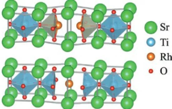
半導体酸化物の透明性やバンド構造は一般的に結晶中の 点欠陥や不純物の元素に依存すると言われている。多くの 酸化物のドーピングにおいて、不純物イオンが結晶内のどの サイトに置換するかはイオン半径や価数によって予測できる ものの、ドーピングされた結晶構造を具体的に予測すること は難しい。その点で蛍光 X 線ホログラフィーは有効的な分 析手法であり、不純物イオン周辺の元素の構造を精密に計 測することを可能にする方法である。このホログラフィーの 手法では、図 1 のように、不純物イオンの元素の蛍光 X 線 の角度依存性から、不純物イオン近傍にある元素の散乱強 度を計測している。我々は Rh をドープした SrTiO3の光触 媒の薄膜結晶にこの方法を適用し、Rh4+のドーパントが格 子歪みのない Ti サイトを置換する一方で、Rh3+のドーパン トは酸素サイトで酸素空孔または置換基を有するクラスター 構造を形成することを見出した ( 図 2)。このようなクラスター 構造は Rh:SrTiO3光触媒におけるフォトキャリアの振る舞 いや太陽光を用いた水分解反応に使用される光電極に重要 な役割を担っていることを明らかにした。
The band gap and transport behavior of oxide semiconduc-tors is generally determined by point defects and doping. In many doped oxide systems, the dominant site substitution mechanism can be assumed from the dopant valence and ionic radius, but explicitly determining the dopant site structure is generally impossible. X-ray fluorescence holography is a useful technique in this regard, as it produces directly the atomic positions of the nearest neighbors surrounding a dopant atom. The method is based on measuring the angular distribution of the dopant atom’s fluorescence x-ray intensity (Fig. 1) and solving for the positions of the nearest-neighbor scatterer atoms. We have analyzed the structure of Rh-doped SrTiO3
photocata-lysts and found that while the Rh4+ dopant substitutes at the Ti
site without lattice distortion, a Rh3+ dopant forms clusters with
oxygen vacancies or substitutes at the oxygen site (Fig. 2). Such clustering has a detrimental effect on photocarrier dynamics in Rh:SrTiO3 photocatalysts and photoelectrodes used for the
solar-powered water splitting reaction.
https://www.issp.u-tokyo.ac.jp/maincontents/organization/labs/lippmaa_group.html
リップマー研究室
Lippmaa Group リップマー ミック LIPPMAA, Mikk 教授 Professor研究テーマ
Research Subjects 1. 2. 3. 4. パルスレーザー堆積法による酸化物薄膜そしてヘテロ構造の作製 Growth of thin oxide films and heterostructures by pulsed laser deposition 水分解光電極反応の高効率化に向けた酸化物半導体材料の開発 Development of oxide photoelectrode materials for photocatalytic water splitting 極性材料とマルチフェロイック材料の開発 Polar oxides and multiferroic coupling 酸化物ナノ構造またはナノコンポジット薄膜の合成 Synthesis of nanostructures and nanocomposite thin films図1.(a)Rh3+:SrTiO3と (b)Rh4+:SrTiO3薄膜における Rh 元素の蛍光 X 線強度 の角度分布について。強度分布の違いは Rh イオン周辺の元素の並び方が異なるこ とを意味しており、(b) のパターンはペロブスカイト構造の完全単結晶の構造と一 致している。
Fig. 1. Angular distribution of Rh fluorescence x-ray intensity for (a) Rh3+:SrTiO3 and (b) Rh4+:SrTiO3 thin films. The difference in the patterns
indicates that the arrangement of the Rh nearest-neighbor atoms is different. The pattern in (b) corresponds to a perfect perovskite structure.
図2.低い酸素圧の条件で堆積した Rh3+:SrTiO3薄膜における2種類の欠陥構造 について。( 上 ) 酸素空孔を持つ Rh 酸化物のクラスター ( 下 ) アニオンサイトに おける Rh の置換構造。
Fig. 2. Two main defect cluster types in a Rh3+:SrTiO3 film grown at low
oxygen pressure: (upper) Rh cluster with an oxygen vacancy, (lower) Rh sub-stitution at the anion site.