JAIST Repository
https://dspace.jaist.ac.jp/Title
Suppression of the epitaxial growth of Si films in Si heterojunction solar cells by the formation of ultra-thin oxide layers
Author(s) Ohdaira, Keisuke; Oikawa, Takafumi; Higashimine, Koichi; Matsumura, Hideki
Citation Current Applied Physics, 16(9): 1026-1029 Issue Date 2016-06-03
Type Journal Article
Text version author
URL http://hdl.handle.net/10119/16145
Rights
Copyright (C)2016, Elsevier. Licensed under the Creative Commons Attribution-NonCommercial-NoDerivatives 4.0 International license (CC BY-NC-ND 4.0).
[http://creativecommons.org/licenses/by-nc-nd/4.0/] NOTICE: This is the author's version of a work accepted for publication by Elsevier. Keisuke Ohdaira, Takafumi Oikawa, Koichi Higashimine, and Hideki Matsumura, Current Applied Physics, 16(9), 2016, 1026-1029, http://dx.doi.org/10.1016/j.cap.2016.06.001 Description
Suppression of the epitaxial growth of Si films in Si heterojunction solar
cells by the formation of ultra-thin oxide layers
Keisuke Ohdaira*, Takafumi Oikawa, Koichi Higashimine, and Hideki Matsumura
Japan Advanced Institute of Science and Technology, 1-1 Asahidai, Nomi, Ishikawa 923-1292, Japan
Abstract
The epitaxial growth of silicon (Si) films during the catalytic chemical vapor deposition (Cat-CVD) of intrinsic amorphous Si (i-a-Si) passivation films on crystalline Si (c-Si) wafers is suppressed by the oxidation of c-Si surfaces simply by dipping the c-Si wafers in hydrogen peroxide (H2O2). This oxidation treatment is also effective for
(111)-oriented c-Si surfaces particularly at high a-Si deposition temperatures. The suppression of the epitaxial growth leads to the better effective minority carrier lifetime (τeff) of c-Si wafers passivated with Cat-CVD i-a-Si films. SHJ solar cells show
remarkably high open-circuit voltage (Voc) exceeding 0.7 V. These results clearly
show the effectiveness of the insertion of SiOx layers on the improvement in Cat-CVD
a-Si/c-Si interfaces.
*Corresponding author. Japan Advanced Institute of Science and Technology, 1-1
Asahidai, Nomi, Ishikawa 923-1292, Japan. E-mail address: [email protected] (K. Ohdaira).
1. Introduction
Silicon heterojunction (SHJ) solar cells have been expected to be one of the most promising next-generation solar cell structures because of its high open-circuit voltage (Voc) and resulting superior performance at high operation temperatures [1-7]. The
high Voc of the SHJ solar cells originates from high-quality hydrogenated amorphous
silicon (a-Si)/crystalline Si (c-Si) interfaces owing to the high passivation ability of a-Si films. Needless to say, the deposition of a-Si films on c-Si wafers must be carefully performed to realize sufficiently low surface recombination velocity (SRV). Plasma-enhanced chemical vapor deposition (PECVD), most widely utilized technique for a-Si deposition, generally requires special care to suppress plasma damage during a-Si deposition onto c-Si surfaces [8,9]. Catalytic CVD (Cat-CVD), often also referred to as hot-wire CVD, can form a-Si films by decomposing source gases on a heating metal wire through catalytic reaction, and hence, can realize the plasma-damage-less deposition of a-Si films [10]. Cat-CVD can thus provide high-quality passivation films on c-Si surfaces, and we have so far actually demonstrated the formation of Cat-CVD high-quality passivation films with low SRV [11-18].
The formation of epitaxial layers during the deposition of a-Si films is another phenomenon which should be avoided for the realization of high-quality passivation films because a large number of defects are included inside them [19]. The epitaxial layers tend to be formed more easily by Cat-CVD than by PECVD [20]. One possible reason of this may be the difference of gas decomposition mechanism. Many kinds of radicals, such as SiH3, SiH2, and SiH, are formed through the collision of electrons with
silane (SiH4) molecules in PECVD [21]. On the other hand, SiH4 radicals are
formation of low-quality epitaxial layers on c-Si. Hence, the suppression of the epitaxial growth is particularly important for the deposition of a-Si passivation films by Cat-CVD. One way to prevent the epitaxial growth is to erase the periodicity of Si crystal on the surface by the formation of a very thin different material. Thin Si oxide (SiOx) is the most promising candidate for such a material because it can be formed
simply by the oxidation of c-Si surfaces. Our approach is to form ultra-thin oxide layers by dipping in liquid oxidant [11]. We have already confirmed that the epitaxial growth on Si(100) can be suppressed by the formation of SiOx layers by dipping in
hydrogen peroxide (H2O2) [11]. The effect of the formation of SiOx layers, however,
may affect differently on different surface orientations. In particular, the effect on Si(111) is more important since it appears on the facet of pyramid textures formed by alkali etching. In this study, we have attempted to clarify the effect of the oxidation of c-Si wafers by H2O2 on the suppression of epitaxial growth and resulting improvement
in the passivation quality of Cat-CVD a-Si films.
2. Experimental procedures
We used (100) and (111)-orientated double-side-polished floating-zone n-type c-Si wafers. The wafers had a resistivity of ~2 Ωcm, thickness of 290 μm, and a bulk lifetime of >10 ms. We first cut the c-Si wafers into 2×2 cm2-sized square-shaped pieces,
and removed native oxide layers on the Si wafers in a 5% HF solution. We then immediately dipped the c-Si wafers in 4 wt% H2O2 for 30 s at room temperature for the
formation of the ultra-thin SiOx layers on their surfaces. The analysis of the ultra-thin
SiOx films by spectroscopic ellipsometry (SE) revealed their thickness to be 0.8-1.0 nm.
temperatures on both sides of the c-Si wafers with and without the ultra-thin SiOx layers
to investigate the effect of SiOx formation on epitaxial growth and passivation quality.
We employed a deposition pressure and a SiH4 flow rate of 1.0 Pa and 10 sccm,
respectively, for the deposition of i-a-Si films. A tungsten wire heated at 1800 °C was used as a catalyzer for the decomposition of SiH4 gas molecules. The c-Si wafers coated
with the i-a-Si passivation films were then annealed at 200 °C for 30 min in air for the improvement in the quality of i-a-Si/c-Si interfaces. If the epitaxial growth takes place on the c-Si, the epitaxially-grown layers have the same optical property as c-Si, and cannot thus be optically distinguished. Hence, we used SE as a method to evaluate a degree of epitaxial growth. We also visualized Cat-CVD a-Si/c-Si interfaces by cross-sectional transmission electron microscopy (TEM). The passivation ability of Cat-CVD i-a-Si films was characterized through the effective minority carrier lifetime (τeff) of the c-Si wafers with i-a-Si films measured by the microwave photoconductivity
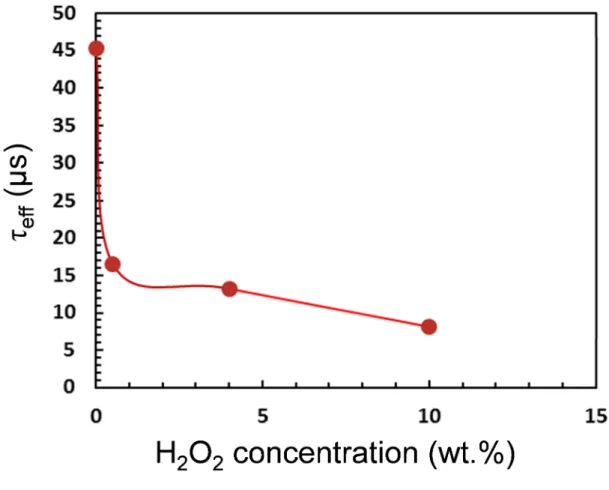
decay (µ-PCD) method. It should be noted that the ultra-thin SiOx layers formed by
dipping in H2O2 do not have any passivation ability. Figure 1 shows the τeff of c-Si
wafers with only ultra-thin SiOx films (without i-a-Si passivation films) as a function of
H2O2 concentration during oxidation process. τeff values are significantly low and
rather decreases by the introduction of oxidation process. The formation of ultra-thin SiOx films is thus only for the suppression of the epitaxial growth.
For the fabrication of SHJ solar cells, we deposited n-type a-Si (n-a-Si)/i-a-Si films on one side of the c-Si wafers and then p-type a-Si (p-a-Si)/i-a-Si films on the other side. PH3 and B2H6 gases diluted with helium to 2.25% were used to deposit the doped a-Si
films. We then formed 80-nm-thick indium tin oxide (ITO) films on the both sides of the c-Si wafers by sputtered at a substrate temperature of 100 °C, followed by the formation
of comb-shaped Ag electrodes by screen printing and successive annealing in air at 200 °C. The SHJ solar cells without the oxidation of c-Si surfaces were also fabricated for comparison. The area of the SHJ cells was 2.25 cm2. The detailed deposition conditions of the a-Si films have been summarized elsewhere [11]. The current density-voltage (J-V) characteristics of the SHJ solar cells fabricated were measured under 1-sun (AM1.5, 100 mW/cm2) illumination. We also characterized the SHJ solar cells by internal quantum efficiency (IQE).
3. Results and discussion
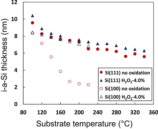
Figure 2 show the SE-measured thickness of Cat-CVD i-a-Si films deposited on (100)- and (111)-oriented c-Si wafers as a function of substrate temperature during i-a-Si deposition. The SE-measured thickness of i-a-Si films on (100)-oriented c-Si wafers without the ultra-thin SiOx formation decreases significantly with increase in the
substrate temperature. This indicates the emergence of epitaxial growth during a-Si deposition. The (100)-oriented c-Si wafers with the ultra-thin SiOx layers do not show
such a serious reduction in the SE-measured i-a-Si thickness, indicating the suppression of the epitaxial growth by the introduction of the ultra-thin SiOx layers. This fact has
been reported in our previous literature [11]. On the contrary, (111)-oriented c-Si wafers do not show the serious reduction of SE-measured i-a-Si film thickness even without the formation of SiOx layers particularly at low substrate temperatures. This
result may correspond to the general nature of Si(111) surfaces with more tolerance for the epitaxial growth [19]. However, larger SE-measured i-a-Si thickness is confirmed on the (111)-oriented c-Si wafers with the ultra-thin SiOx layers than those without SiOx
of SiOx layers is also effective for (111)-oriented c-Si surfaces particularly at high
substrate temperatures.
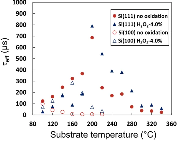
Figure 3 shows the τeff of (100)- and (111)-oriented c-Si wafers with Cat-CVD i-a-Si
passivation films as a function of substrate temperature. τeff values are quite low for
(100)-oriented c-Si wafers without SiOx layers, while much higher τeff values are
obtained for the c-Si wafers with SiOx layer formation [11]. This fact shows the
improvement in the quality of a-Si/c-Si interfaces by the introduction of the ultra-thin SiOx films. On the contrary, there is no clear difference between the τeff values of
(111)-oriented c-Si wafers with and without ultra-thin SiOx films at low deposition
temperatures. This is consistent with the result shown in Fig. 1, which indicates the absence of epitaxial growth at low deposition temperature. At high deposition temperatures (>200 °C), the τeff values of (111)-oriented c-Si wafers with the ultra-thin
SiOx layers are always higher than those without the SiOx layers. This means the
better a-Si/c-Si interface quality on the c-Si wafers with SiOx layers resulting from the
suppression of the epitaxial growth.
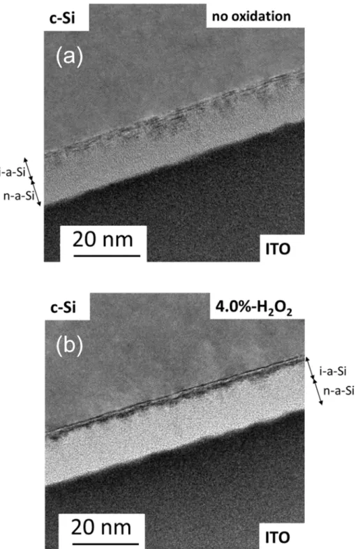
Figure 4 shows the cross-sectional TEM images of a-Si/Si(111) interfaces without and with ultra-thin oxide layers. The i-a-Si films were deposited at 240 °C in order to clearly see the effectiveness of the formation of SiOx layers. An epitaxial layer is
definitely seen in the vicinity of an a-Si/c-Si interface on the c-Si wafer without a SiOx
layer, while only much thinner epitaxial layer is observed on the c-Si wafer with a SiOx
layer. This is also a clear experimental evidence of the suppression of epitaxial growth by the usage of ultra-thin SiOx layers.
Figure 5 shows the J-V characteristics of SHJ solar cells fabricated using Si(111) wafers without and with SiOx oxide layers. We also used i-a-Si films deposited at
240 °C in the SHJ solar cells. Their performances are summarized in Table I. The short-circuit current density (Jsc) and fill factor (FF) of the SHJ cells are not sufficiently
high. The low Jsc is because not alkali-textured but mirror-polished c-Si wafers were
used for the SHJ cells and anti-reflection effect is imperfect. The insufficient FF is due to high series resistance, which is confirmed from high pseudo FF (pFF) values of >0.8 obtained by Suns-Voc measurement. One of the possible reasons for the high FFs is unoptimized ITO resistivity. The lower FF in the cell with SiOx layers indicates that
the SiOx layers and/or thicker a-Si films can also act to increase series resistance.
Similar tendency has also been confirmed for the cells with (100)-oriented wafers [11]. Note that this work does not aim at the realization of high-performance solar cells but simply focuses on the effect of oxidation process on the suppression of epitaxial growth. It should be emphasized that the SHJ cells with the ultra-thin SiOx layers have higher
τeff and Voc than that without SiOx layers. These values are ~2.5 ms and >0.7 V,
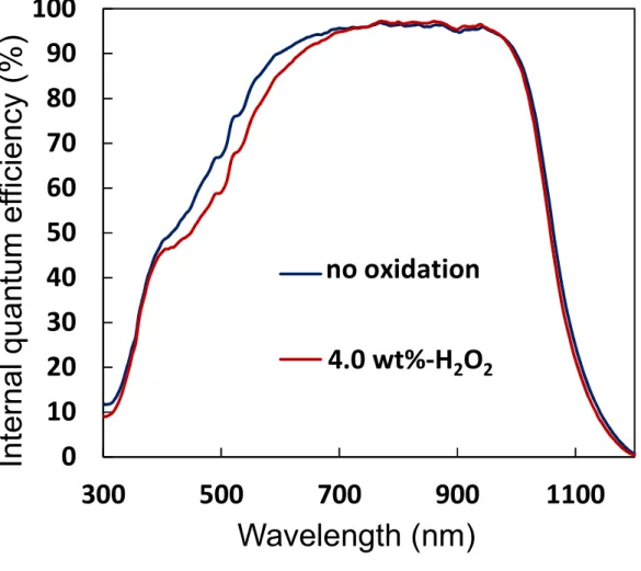
respectively, indicating the excellent quality of a-Si/c-Si interfaces. Figure 6 shows the IQE spectra of the SHJ solar cells fabricated using Si(111) wafers without and with SiOx
oxide layers. Significantly low IQE region is confirmed in the wavelength of less than 600 nm, which is probably due to parasitic optical absorption in a-Si films formed on the illuminated side of c-Si wafers. Lower IQE is seen in the SHJ solar cell with SiOx
layers, which is consistent with the lower Jsc of SHJ cell with SiOx layers shown in Fig.
5. This may be because of the existence of thicker i-a-Si films due to suppressed epitaxial growth. Note that this low Jsc will be easily improved by optimizing the
thickness of i-a-Si and p-a-Si films. Based on the results obtained in this study, we can conclude that the oxidation of (111)-oriented c-Si by the simple H2O2 dipping prior to
to improve the quality of a-Si/c-Si interfaces.
4. Conclusions
We have investigated the effectiveness of the H2O2 oxidation of (111)-oriented c-Si
surfaces on the suppression of the epitaxial growth of Si films. The epitaxial growth can be prevented by the formation of ultra-thin SiOx layers also on Si(111) surfaces
particularly at substrate temperature of more than 200 °C during i-a-Si deposition. The suppression of epitaxial growth leads to better τeff values, indicating improvement in
a-Si/c-Si interface qualities. The SHJ solar cell with the ultra-thin SiOx layers shows
better Voc than that without SiOx layers, demonstrating the effect of SiOx insertion also
on actual solar cell devices.
Acknowledgments
References
[1] M. Taguchi, A. Yano, S. Tohoda, K. Matsuyama, Y. Nakamura, T. Nishiwaki, K. Fujita, E. Maruyama, 24.7% Record efficiency HIT solar cell on thin silicon wafer, IEEE J. Photovoltaics 4 (2014) 96.
[2] K. Masuko, M. Shigematsu, T. Hashiguchi, D. Fujishima, M. Kai, N. Yoshimura, T. Yamaguchi, Y. Ichihashi, T. Mishima, N. Matsubara, T. Yamanishi, T. Takahama, M. Taguchi, E. Maruyama, S. Okamoto, Achievement of more than 25% conversion efficiency with crystalline silicon heterojunction solar cell, IEEE J. Photovoltaics 4 (2014) 1433.
[3] J. Nakamura, N. Asano, T. Hieda, C. Okamoto, H. Katayama, K. Nakamura, Development of heterojunction back contact Si solar cells, IEEE J. Photovoltaics 4, 1491 (2014).
[4] S. De Wolf, A. Descoeudres, Z. C. Holman, C. Ballif, High-efficiency silicon heterojunction solar cells: a review, Green 2 (2012) 7.
[5] J. L. Hernández, D. Adachi, D. Schroos, N. Valckx, N. Menou, T. Uto, M. Hino, M. Kanematsu, H. Kawasaki, R. Mishima, K. Nakano, H. Uzu, T. Terashita, K. Yoshikawa, T. Kuchiyama, M. Hiraishi, N. Nakanishi, M. Yoshimi, K. Yamamoto, High efficiency copper electroplated heterojunction solar cells and modules – the path towards 25% cell efficiency, Proc. 28th European Photovolt. Solar Energy Conf., 2013, p. 741.
[6] A. Descoeudres, Z. C. Holman, L. Barraud, S. Morel, S. De Wolf, C. Ballif, >21% Efficient Silicon Heterojunction Solar Cells on n- and p-Type Wafers Compared, IEEE J. Photovolt. 3 (2013) 83.
[7] M. Taguchi, A. Terakawa, E. Maruyama, M. Tanaka, Obtaining a Higher Voc in HIT
[8] D. Sarkar, E. U. Onyegam, S. Saha, L. Mathew, R. A. Rao, M. M. Hilali, R. S. Smith, D. Xu, D. Jawarani, R. Garcia, R. Stout, A. Gurmu, M. Ainom, J. G. Fossum, S. K. Banerjee, Remote Plasma Chemical Vapor Deposition for High-Efficiency Ultra-Thin ~25-Microns Crystalline Si Solar Cells, Proc. 38th IEEE Photovoltaic Specialists Conf., 2012.
[9] H. Matsumura, K. Higashimine, K. Koyama, K. Ohdaira, Comparison of crystalline-silicon/amorphous-silicon interface prepared by plasma enhanced chemical vapor deposition and catalytic chemical vapor deposition, J. Vac. Sci. Technol. B 33 (2015) 031201.
[10] H. Matsumura, Catalytic chemical vapor deposition method producing high quality hydrogenated amorphous silicon, Jpn. J. Appl. Phys. 25 (1986) L949.
[11] T. Oikawa, K. Ohdaira, K. Higashimine, H. Matsumura, Application of crystalline silicon surface oxidation to silicon heterojunction solar cells, Current Appl. Phys. 15 (2015) 1168.
[12] S. Tsuzaki, K. Ohdaira, T. Oikawa, K. Koyama, H. Matsumura, Improvement in passivation quality and open-circuit voltage in silicon heterojunction solar cells by the catalytic doping of phosphorus atoms, Jpn. J. Appl. Phys. 54 (2015) 072301.
[13] Trinh Cham Thi, K. Koyama, K. Ohdaira, H. Matsumura, Drastic reduction in the surface recombination velocity of crystalline silicon passivated with Cat-CVD SiNx
films by introducing phosphorous Cat-doped layer, J. Appl. Phys. 116 (2015) 044510. [14] Trinh Cham Thi, K. Koyama, K. Ohdaira, H. Matsumura, Passivation quality of a stoichiometric SiNx single passivation layer on crystalline silicon prepared by Cat-CVD
and successive annealing, Jpn. J. Appl. Phys. 53 (2014) 022301.
Effect of radical-doped n+ back surface field layer on the effective minority carrier lifetimes in crystalline Si with amorphous Si passivation Layer deposited by catalytic chemical vapor deposition, Jpn. J. Appl. Phys 51 (2012) 101301.
[16] Trinh Cham Thi, K. Koyama, K. Ohdaira, H. Matsumura, Passivation characteristics of SiNx/a-Si and SiNx/Si-rich SiNx stacked layers on crystalline silicon,
Sol. Energy Mater. Sol. Cells 100 (2012) 169.
[17] H. Matsumura, M. Miyamoto, K. Koyama, K. Ohdaira, Drastic reduction in surface recombination velocity of crystalline silicon by surface treatment using catalytically-generated radicals, Sol. Energy Mater. Sol. Cells 95 (2011) 797.
[18] K. Koyama, K. Ohdaira, H. Matsumura, Extremely low surface recombination velocities on crystalline silicon wafers realized by catalytic chemical vapor deposited SiNx/a-Si stacked passivation layers, Appl. Phys. Lett. 97 (2010) 082108.
[19] U. K. Das, M. Z. Burrows, M. Lu, S. Bowden, R. W. Birkmire, Surface passivation and heterojunction cells on Si (100) and (111) wafers using dc and rf plasma deposited Si:H thin films, Appl. Phys. Lett. 92 (2008) 063504.
[20] Qi Wang, M. Page, Y. Ai, W. Nemeth, L. Roybal, H.-C. Yuan, Hydrogenated amorphous Si deposition for high efficiency a-Si/c-Si heterojunction solar cells, Proc. 39th IEEE Photovolt. Specialists Conf., 2012, p. 188.
[21] A. Matsuda, Thin-film silicon –growth process and solar cell application–, Jpn. J. Appl. Phys. 43 (2004) 7909.
[22] S. Tange, K. Inoue, K. Tonokura, M. Koshi, Catalytic decomposition of SiH4 on a
Figure captions
Fig. 1 τeff of bare c-Si wafers with ultra-thin SiOx films as a function of H2O2
concentration.
Fig. 2 SE-measured thickness of Cat-CVD i-a-Si films deposited on (100)- and (111)-oriented c-Si wafers as a function of substrate temperature.
Fig. 3 τeff of (100)- and (111)-oriented c-Si wafers with Cat-CVD i-a-Si passivation
films as a function of substrate temperature.
Fig. 4 Cross-sectional TEM images of a-Si/Si(111) interfaces (a) without and (b) with ultra-thin oxide layers.
Fig. 5 J-V characteristics of SHJ solar cells fabricated using Si(111) wafers without and with SiOx oxide layers.
Fig. 6 IQE spectra of SHJ solar cells fabricated using Si(111) wafers without and with SiOx oxide layers.
Figure 2 K. Ohdaira et al.,
0
2
4
6
8
10
12
80
120
160
200
240
280
320
360
iiii----aaaa
----S
i
S
i
S
i
S
i
-4.0% -4.0%i-a
-S
i
th
ickn
e
ss
(n
m
)
Substrate temperature (
°C)
Figure 3 K. Ohdaira et al.,
0
100
200
300
400
500
600
700
800
900
1000
80
120
160
200
240
280
320
360
-4.0%
-4.0%
Substrate temperature (
°C)
τ
e
ff
(µ
s
)
Figure 5 K. Ohdaira et al.,
0
5
10
15
20
25
30
35
0
0.1
0.2
0.3
0.4
0.5
0.6
0.7
0.8
C
u
rr
e
n
t
d
e
n
si
ty
/
m
A
C
u
rr
e
n
t
d
e
n
si
ty
/
m
A
C
u
rr
e
n
t
d
e
n
si
ty
/
m
A
C
u
rr
e
n
t
d
e
n
si
ty
/
m
A
cmcmcmcm
----2222no oxidation
4.0 wt%-H
2O
2C
u
rr
e
n
t
d
e
n
s
it
y
(
m
A
/c
m
2
)
Voltage (V)
Figure 6 K. Ohdaira et al.,