®
Using the ClockLock &
ClockBoost PLL Features
in APEX Devices
April 2000, ver. 2.0 Application Note 115
Introduction
APEXTM 20K devices have the ClockLockTM and ClockBoostTM features, which use phase-locked loops (PLLs) to increase performance and provide clock-frequency synthesis. The ClockLock feature minimizes clock delay and clock skew within the device, reducing clock-to-output and setup times while maintaining zero hold times. The ClockBoost feature allows designers to run the internal logic of the device at a faster or slower rate than the input clock frequency. This technique simplifies board design because the clock tree on the board does not have to distribute a high-speed signal. Through the use of time-domain multiplexing, the ClockBoost feature allows the designer to improve device area efficiency by sharing resources within the device.APEX 20KE devices include PLLs with an enhanced ClockLock feature set, such as advanced ClockBoost capability for m/(n´k) multiplication, low-voltage differential signaling (LVDS) support, external clock outputs and feedback ability, and ClockShiftTM circuitry for more complex clock- frequency synthesis applications. These enhanced features permit system- level clock management and skew control in APEX 20KE devices.
The ClockLock and ClockBoost features provide significant
improvements in system performance, bandwidth, and system-on-a- programmable-chip integration. This application note explains the APEX 20K and APEX 20KE ClockLock and ClockBoost features. It also describes common applications for these features.
Clock Delay &
Skew
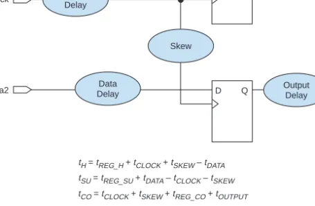
The delay from a clock pin to a register, especially for large devices, can be significant enough to degrade both on- and off-chip performance. The equation for the pin-to-pin clock-to-output delay (tCO) is shown in Figure 1.
The clock delay (tCLOCK) and clock skew (tSKEW) parameters account for a significant portion of the total clock-to-output delay in larger devices. By reducing clock delay and clock skew, the ClockLock and ClockBoost circuitry improves the device’s clock-to-output times.
AN 115: Using the ClockLock & ClockBoost PLL Features in APEX Devices
Figure 1. APEX 20K & APEX 20KE Hold, Setup & Clock-to-Output Times
Clock skew—the difference between clock delays to different registers—
also increases the setup time indirectly. To ensure a zero hold time (tH), add a data delay to account for the longest clock delay to any register. This delay must be long enough to ensure a zero hold time under fast process, voltage, and temperature conditions. However, the added data delay also increases the register’s setup time under slow process, voltage, and temperature conditions. When a ClockLock signal feeds a register, the signal bypasses the data delay element to the register, resulting in a decreased setup time. Because clock skew and delay are reduced, the register maintains a zero hold time.
As programmable logic devices (PLDs) become larger, clock delay and skew can become a problem. Also, clock skew can affect a board design.
To address these issues, designers can use either PLLs or delay-locked loops (DLLs). Although both can reduce the skew within system clocks, PLLs are more flexible than DLLs for frequency synthesis of system clocks. In addition, DLLs are not capable of performing non-integer scaling, and they cannot attenuate input jitter. In DLLs, all input jitter propagates to the output and accumulates when the DLLs are cascaded.
PLLs are ideal for clock multiplication and division applications, because they can perform non-integer scaling.
D Q
D Q
data1
clock
data2
tH = tREG_H + tCLOCK + tSKEW – tDATA tSU = tREG_SU + tDATA – tCLOCK – tSKEW tCO = tCLOCK + tSKEW + tREG_CO + tOUTPUT
Data Delay
Data Delay Clock Delay
Skew
Output Delay Output Delay
AN 115: Using the ClockLock & ClockBoost PLL Features in APEX Devices Table 1 shows the features for APEX 20K and APEX 20KE devices.
Notes:
(1) APEX 20K devices that support ClockLock and ClockBoost features are denoted by an “X” suffix in the ordering code (e.g., EP20K400FC672-1X).
(2) m is an integer that ranges from 1 to 160.
(3) The quantity (n´k) can range from 1 to 160. A special multiplication rate is also provided for T1 to E1 frequency conversion (i.e., 256/193), and E1 to T1 frequency conversion (i.e., 193/256).
(4) The EP20K300E device supports LVDS data transfer at up to 155 megabits per second (Mbps).
APEX 20K Devices
APEX 20K devices have one PLL that features ClockLock and ClockBoost circuitry. This PLL can be instantiated by using the altclklock
megafunction. APEX 20K devices support ClockBoost multiplication circuitry, offering 1´, 2´, and 4´ clock multiplication. Figure 2 shows the ClockLock and ClockBoost circuitry block diagrams within the
altclklock megafunction and its ports.
Table 1. APEX 20K & APEX 20KE ClockLock Features Note (1) Device Number
of PLLs
ClockBoost Feature
Number of External
Clock Outputs
Number of Feedback Inputs
ClockShift T1/E1 Conversion
LVDS Clock
LVDS Data
EP20K100 1 1´, 2´, 4´ – – – – – –
EP20K200 1 1´, 2´, 4´ – – – – – –
EP20K400 1 1´, 2´, 4´ – – – – – –
EP20K100E 2 m/(n´k) (2), (3) 1 1 v v v –
EP20K160E 2 m/(n´k) (2), (3) 1 1 v v v –
EP20K200E 2 m/(n´k) (2), (3) 1 1 v v v –
EP20K300E 4 m/(n´k) (2), (3) 2 2 v v v (4)
EP20K400E 4 m/(n´k) (2), (3) 2 2 v v v v
EP20K600E 4 m/(n´k) (2), (3) 2 2 v v v v
EP20K1000E 4 m/(n´k) (2), (3) 2 2 v v v v
AN 115: Using the ClockLock & ClockBoost PLL Features in APEX Devices
Figure 2. ClockLock & ClockBoost Circuitry in APEX 20K Devices
Note:
(1) This division is used only for the purpose of dividing down a 2´/4´clock1 to obtain a 1´/2´/4´ on clock0.
You can use a single output clock of 1´, 2´, 4´, or any combination of output clocks. Table 2 describes the clock multiplication combinations that the altclklock megafunction supports for APEX 20K devices.
The dedicated clock pin (CLK2) supplies the clock to the PLL and the altclklock megafunction. Adhere to the following guidelines when using the altclklock megafunction in APEX 20K devices:
■ The inclock port must only be fed directly by the dedicated clock input pin (CLK2) without inversion.
■ altclklock can only be used to clock positive or negative edge- triggered registers in logic elements (LEs), I/O elements (IOEs), or embedded system blocks (ESBs). IOE registers can only have single clock polarity from a given altclklock output (i.e., IOE registers must be all positive-edge triggered or all negative-edge triggered). If both clock polarities are needed for IOE, use two PLL outputs.
■ The CLK2 pin that directly feeds the inclock port can also drive other registers without the PLL. However, doing so makes the CLK1 pin and the clock1 port unavailable.
■ When two PLL outputs are used, the other clock pin ( ) cannot be
Ö 1, 2, or 4 Phase
Comparator
Voltage-Controlled Oscillator
ClockBoost
altclklock Megafunction
inclock Ö 1, 2, or 4 clock0
clock1 (1)
Table 2. Multiplication Factor Combinations
Clock 0 Clock 1 Input Frequency (MHz)
-1X Speed Grade -2X Speed Grade
1´ 2´ 25 to 180 25 to 170
1´, 2´ 4´ 16 to 90 16 to 100
1´, 2´, 4´ 4´ 10 to 48 10 to 34
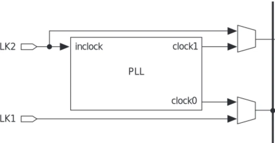
You should connect the board clock trace to only the CLK2 pin for designs that require two outputs from the altclklock megafunction. Figure 3 illustrates the valid clock connections for the PLL and global clock lines.
Figure 3. APEX 20K Dedicated Global Clock Pin Connections to PLL & Dedicated Clock Lines
Table 3 shows the timing parameters for the APEX 20K ClockLock and ClockBoost features.
PLL inclock
clock0 clock1 CLK2
CLK1
Dedicated Clocks
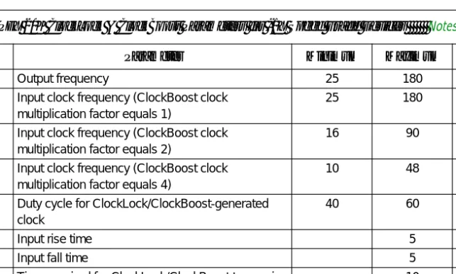
Table 3. APEX 20K ClockLock & ClockBoost Parameters for -1X Speed Grade Devices Notes (1), (2)
Symbol Parameter Minimum Maximum Unit
fOUT Output frequency 25 180 MHz
fCLK1 Input clock frequency (ClockBoost clock multiplication factor equals 1)
25 180 MHz
fCLK2 Input clock frequency (ClockBoost clock multiplication factor equals 2)
16 90 MHz
fCLK4 Input clock frequency (ClockBoost clock multiplication factor equals 4)
10 48 MHz
tOUTDUTY Duty cycle for ClockLock/ClockBoost-generated clock
40 60 %
tR Input rise time 5 ns
tF Input fall time 5 ns
tLOCK Time required for ClockLock/ClockBoost to acquire lock (3)
10 µs
Notes to tables:
(1) This information is preliminary.
(2) All input clock specifications must be met. The PLL may not lock onto an incoming clock if the clock specifications are not met, creating an erroneous clock within the device.
(3) During device configuration, the ClockLock and ClockBoost circuitry is configured first. If the incoming clock is supplied during configuration, the ClockLock and ClockBoost circuitry locks during configuration, because the lock time is less than the configuration time.
(4) The jitter specification is measured under long-term observation.
(5) If the input clock stability is 100 ps, tJITTER is 250 ps.
Table 5 lists the APEX 20K ClockLock pins and their function.
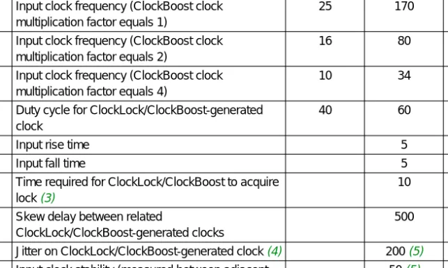
Table 4. APEX 20K ClockLock & ClockBoost Parameters for -2X Speed Grade Devices Notes (1), (2)
Symbol Parameter Minimum Maximum Unit
fOUT Output frequency 25 170 MHz
fCLK1 Input clock frequency (ClockBoost clock multiplication factor equals 1)
25 170 MHz
fCLK2 Input clock frequency (ClockBoost clock multiplication factor equals 2)
16 80 MHz
fCLK4 Input clock frequency (ClockBoost clock multiplication factor equals 4)
10 34 MHz
tOUTDUTY Duty cycle for ClockLock/ClockBoost-generated clock
40 60 %
tR Input rise time 5 ns
tF Input fall time 5 ns
tLOCK Time required for ClockLock/ClockBoost to acquire lock (3)
10 µs
tSKEW Skew delay between related
ClockLock/ClockBoost-generated clocks
500 ps
tJITTER Jitter on ClockLock/ClockBoost-generated clock (4) 200 (5) ps tINCLKSTB Input clock stability (measured between adjacent
clocks)
50 (5) ps
Notes:
(1) LVCMOS: low-voltage complementary metal-oxide semiconductor; LVTTL: low-voltage transistor-to-transistor logic; PCI: peripheral component interconnect.
(2) APEX 20K devices with a -V ordering code suffix are 5.0-V tolerant.
APEX 20KE Devices
APEX 20KE devices incorporate multiple ClockLock circuits with advanced features. These features include ClockLock circuitry, advanced ClockBoost circuitry, LVDS support, ClockShift circuitry, and external clock outputs with optional external feedback inputs.
Advanced ClockBoost Multiplication & Division
Each APEX 20KE PLL includes circuitry that provides clock synthesis for two outputs using m/(n ´ k) and m/(n ´ v) scaling factors. When a PLL is locked, the locked output clock aligns to the rising edge of the input clock.
The closed loop equation for Figure 3 gives an output frequency of fCLOCK0 = (m/(n ´ k)) fIN and fCLOCK1 = (m/(n ´ v))fIN. This equation allows the multiplication or division of clocks by a programmable number. The Quartus software automatically chooses the appropriate scaling factors (m, n, k, and v) according to the frequency, multiplication, and division values entered.
The scaling multiplication of APEX 20KE PLLs allows for a wide range of user-defined multiplication and division ratios that are not possible with DLLs. For example, if a frequency scaling factor of 3.75 is needed for a given input clock, you can enter a multiplication factor of 15 and a division factor of 4. Because this advanced ClockBoost scaling can be Table 5. APEX 20K Device ClockLock Pins
Pin Name Pin Type Description I/O Standard
Supported (1) CLK2 Input Dedicated pin that drives the ClockLock and
ClockBoost circuitry.
2.5-V I/O, LVCMOS, LVTTL, 3.3-V PCI, CMOS (2), TTL (2) LOCK Output Optional pin that shows the status of the ClockLock
and ClockBoost circuitry. When the ClockLock and ClockBoost circuitry is locked to the incoming clock and generates an internal clock, LOCK is driven high.
LOCK remains high as long as the clock input remains within specification.
All APEX 20KE PLLs are capable of converting between T1 and E1 clock frequencies. The T1 telecommunications standard uses a 1.544-MHz clock, and the E1 telecommunications standard uses a 2.048-MHz clock.
APEX 20KE PLLs can convert a T1 frequency to an E1 frequency and vice versa.
LVDS Interface
In EP20K400E and larger devices, two of the ClockLock PLLs can be configured for use in LVDS transmitter and receiver interfaces. When the PLL is configured to use LVDS, the I/O clock can be multiplied to support high-speed data transfer rates and to convert between LVDS and CMOS data. These PLLs interface with the APEX 20KE LVDS receiver and LVDS transmitter blocks.
f
See Application Note 120 (Using LVDS in APEX 20KE Devices) for more information on LVDS.External Clock Outputs
In EP20K300E and larger devices, low-jitter external clocks, CLKLK_OUT1P and CLKLK_OUT2P, are available for external clock sources. In EP20K30E, EP20K60E, EP20K100E, EP20K160E, and EP20K200E devices, one external clock, CLKLK_OUT2P, is available for an external clock source. The CLKLK_OUT1P signal originates from PLL 1; the CLKLK_OUT2P signal originates from PLL 2. Other devices on the board can use these outputs as clock sources.
External clock outputs are available in three modes:
■ Zero Delay Buffer—The external clock output pin is phase aligned with the clock input pin for zero delay. Phase shift is not allowed in this configuration. Clock division is possible on the external clock output in this configuration. Multiplication is possible on the remaining PLL output that is not driven off-chip. The altclklock megafunction’s MegaWizard Plug-In should be used to verify possible clock settings.
■ External Feedback—The external feedback input pin is phase aligned with the clock input pin. By aligning these clocks, you can actively remove clock delay and skew between devices. This mode has the same restrictions as the zero delay buffer.
■ Normal Mode—The external clock output pin will have phase delay relative to the clock input pin. If an internal clock is used in this mode, it will be phase aligned to the input clock pin.
ClockShift Circuitry
APEX 20KE PLLs have ClockShift circuitry that provides programmable clock delay and phase shift. The user enters the desired phase shift. Phase shifts of 90˚, 180˚, and 270˚ can be implemented exactly. Other phase shift or delay shift values (in time units) are available with a 0.5 ns to 1.0 ns resolution range. This resolution varies with frequency input and the user-entered multiplication and division factors. The ClockShift circuitry can only be used on a multiplied or divided clock if the input and output frequency have an integer multiple relationship (i.e., fIN/fOUT or fOUT/fIN must be an integer). The PLL ClockShift circuitry is only available in Normal mode.
Clock Enable Signal
APEX 20KE PLLs have a CLKLK_ENA pin for enabling and disabling all of the device PLLs. When the CLKLK_ENA pin is high, the PLL drives the clock0 and clock1 ports. When the CLKLK_ENA pin is low, the clock0 and clock1 ports are driven by GND and all of the PLLs go out of lock.
When the CLKLK_ENA pin goes high again, the PLL must relock.
The individual enable port on the altclklock megafunction is an all-or- none control signal. If the enable port is used for any altclklock instance, all other instances must use the enable port and connect to the same pin. If the port is used, the pin connected to the enable ports must be the CLKLK_ENA dedicated pin.
The inclocken input port on the altclklock megafunction should be used for all designs. If the CLKLK_ENA control is needed by the designer, it must be brought to the CLKLK_ENA input pin. The Quartus software automatically assigns the pin location to this dedicated function pin.
If the CLKLK_ENA control is not needed by the user in Zero Delay Buffer and Normal modes, the inclocken port should not be connected to an input pin in the design. On the board, this pin can be connected to VCC or GND since it will be a floating input.
If the CLKLK_ENA control is not needed by the user in External Feedback mode, the inclocken port must be connected to an input pin. On the board, the user must connect this pin directly to the INIT_DONE pin. The INIT_DONE option must be set in the Device & Pin Options tab of the Compiler Settings > Chips & Devices dialog box (Processing menu). If system control over the CLKLK_ENA pin is needed in External Feedback
Figure 4. Wire-ANDing with the Open-Drain INIT_DONE Pin
Lock Signals
The APEX 20KE ClockLock PLL circuits support individual LOCK signals.
The LOCK signal drives high when the PLL has locked onto the input clock.
LOCK remains high as long as the input remains within specification. It will go low if the input is out of specification. When using two clock outputs from a PLL, the two outputs may become valid at different times.
This difference is caused by the difference in divider ratios between the two outputs. A LOCK pin is optional for each PLL used in APEX 20KE devices; when not used, they are I/O pins. This signal is not available internally. If this signal is used in the design, it must be fed back in with an input pin.
Before configuration, all PLL circuits are disabled and powered down.
During configuration, the PLLs are disabled. When the device goes into user mode, the lock time is measured from the CLKLK_ENA rising edge to the LOCK rising edge.
During device programming, the I/O standard of each I/O pin defaults to 3.3-V LVTTL, which may not be correct. For this reason, the PLL does not lock during configuration.
The LOCK signal indication also has separate programmable latency controls for LOCK assertion and deassertion. Users can select one of two multipliers, 1 or 5, to indicate a small or large latency. The number of half cycles for indication is dependent on the multiplication/division ratio and input frequency. Depending on these factors, the low end of latency ranges from 1 to 16 half-clock cycles; the high end of latency ranges from 5 to 80 half-clock cycles.
The APEX 20KE ClockLock circuits (PLLs) are instantiated using the altclklock megafunctions. Figure 5 shows the ClockLock and ClockBoost circuitry in APEX 20KE devices.
CLKLK_ENA
INIT_DONE VCC
Optional Control Signal
Figure 5. ClockLock & ClockBoost Circuitry in APEX 20KE Devices
Each of the dedicated global clock pins in EP20K300E, EP20K400E, EP20K600E, EP20K1000E, and EP20K1500E devices (CLK1P, CLK2P, CLK3P, CLK4P) supplies the clock to a PLL. Each altclklock instance represents a single PLL instantiation. All altclklock clock outputs are 50/50 duty cycle. The altclklock megafunction in APEX 20KE devices must adhere to the following guidelines:
■ It can only be fed directly by a dedicated clock input pin without inversion.
■ altclklock can only be used to clock positive or negative edge- triggered registers in logic elements (LEs), I/O elements (IOEs), or embedded system blocks (ESBs). IOE registers can only have single clock polarity from a given altclklock output (i.e., IOE registers must be all positive-edge triggered or all negative-edge triggered). If both clock polarities are needed for IOE, use two PLL outputs.
■ The allowable frequency input range is 1.5 to 160 MHz.
■ The allowable frequency output range on clock0 is 1.5 to 200 MHz.
■ The allowable frequency output range on clock1 is 20 to 200 MHz.
■ Phase shifting is only possible on a multiplied clock if the input and output frequency have an integer-multiple relationship (i.e., fIN/fOUT or fOUT/fIN must be an integer).
■ Phase shifting, using degree or time units, will delay or lag the output clock with respect to the input clock (see Figure 6).
■ The ratio of clock_boost to clock_divide cannot be greater than 133. A special scaling ratio of 256/193 or 193/256 is allowed for T1/E1 or E1/T1 clock rate conversion, respectively.
Phase Comparator
Voltage-Controlled Oscillator
altclklock Megafunction
inclock clock0
clock1 Ö n
Ö m
ClockShift Circuitry
Ö k
Ö v fbin
Figure 6. Phase & Delay Shifting Using APEX 20KE PLLs
Several conditions exist that govern the relationship between the input frequency, m, n, k, v, and phase shift values. The altclklock
MegaWizard Plug-In automatically sets the m, n, k, and v dividers to satisfy these equalities and to accommodate the phase shift entered and the clock multiplication or division. The MegaWizard Plug-In verifies the validity of the settings and reports if a multiplication/division frequency ratio is not valid.
Each PLL can be driven by a dedicated clock pin and bypassed simultaneously. The CLK3P and CLK4P pins can feed two PLLs each, or two altclklock instances. This capability is useful for applications that need both phase-shifted and non-phase-shifted versions of the clock.
Because the eight PLL outputs are shared among four possible dedicated global clock lines, certain combinations of multiple altclklock instances and their output connections are not possible. The Quartus software uses different PLLs (i.e., 1, 2, 3, 4) based on pin assignments made to the dedicated global clock pin that feeds the altclklock megafunction.
Figure 7 illustrates the valid clock connections for the PLL and the dedicated global clock lines in these devices. This figure should be used to determine whether a design clocking scheme is valid in terms of
APEX 20KE PLL and clock connections. For example, in an EP20K400E device, CLK4P can feed PLL 4 and PLL 2 simultaneously; however, only a single internal output from each PLL can be used, because the four possible outputs feed two global clock lines.
Figure 7. Dedicated Global Clock Pin Connections to PLL & Dedicated Clock Lines for EP20K300E, EP20K400E, EP20K600E, EP20K1000E & EP20K1500E Devices
Notes:
(1) These PLL connections are used only in LVDS mode and apply to the altlvds megafunction. LVDSTXINCLK, LVDSRXINCLK, and LVDSTXOUTCLK are designated dual-purpose I/O pins that are used as LVDS clocks for the PLLs in LVDS mode. These connections only apply to EP20K400E, EP20K600E, EP20K1000E, and EP20K1500E devices and are mutually exclusive from the general-purpose connections (i.e., inclock, clock0, and clock1).
CLK3p and CLK4p drive drive PLL3 and PLL4, respectively, for general-purpose mode only. LVDSTXINCLK1p and LVDSRXINCLK1p drive PLL3 and PLL4, respectively, for LVDS mode.
(2) PLL 3 or PLL 4 can only be configured for either general-purpose or LVDS use.
(3) This PLL output is a high-speed CMOS/LVDS interface clock that feeds the LVDS transmitter block.
(4) This PLL output is a high-speed LVDS/CMOS interface that feeds the LVDS receiver block.
For EP20K60E, EP20K100E, EP20K160E, and EP20K200E devices, the CLK4P and CLK2P dedicated clock pins supply the clock to two PLLs.
These PLLs have the same usage guidelines as the EP20K400E and larger devices’ PLLs, with the exception of some PLL connections. You can use all four possible PLL output clocks that are shared among four dedicated clock lines. If you use all of the outputs, the CLK3P and CLK1P pins cannot be used.
Figure 8 illustrates the valid clock connections for the PLL and the global clock lines in these devices. Use Figure 8 to determine whether a design clocking scheme is valid in terms of PLL and clock connections. The altclklock megafunction port connections should follow the usage guidelines illustrated in Figures 7 and 8.
4 Dedicated Clocks
CLKLK_FB2p
CLKLK_OUT2p
CLKLK_FB1p
CLKLK_OUT1p CLK3p
CLK1p CLK4p
G1 G2 G3
LVDSRXINCLK1p LVDSTXINCLK1p
LVDSTXOUTCLK1p
CLK2p
(1) (1)
(1) (1)
(1) (1)
(3) (4)
(1)
(2) (2)
tx_outclock 1×
clock1 clock0 PLL4 tx_inclock
inclock
clock1
clock0 inclock PLL2
fbin fbin
rx_outclock clock1 clock0
PLL3 rx_inclock
inclock
clock1
clock0
PLL1 inclock G4
G3 G2
G1
Figure 8. Dedicated Global Clock Pin Connections to PLL & Dedicated Clock Lines for EP20K60E, EP20K100E, EP20K160E & EP20K200E Devices
Table 6 shows the APEX 20K ClockLock and ClockBoost parameters, and Table 7 shows the PLL parameters in LVDS mode.
4 Dedicated Clocks
CLKLK_FB2p
CLKLK_OUT2p CLK4p
CLK2p
clock1 1×
clock0 inclock PLL4
clock1
clock0 inclock PLL2
fbin
G4
G3 G2
G1
CLK3p
CLK1p
Table 6. APEX 20KE ClockLock & ClockBoost PLL Parameters Notes (1), (2), (3)
Symbol Parameter Minimum Typical Maximum Units
fCLOCK0 Output frequency for clock0 output 1.5 200 (4) MHz
fCLOCK1 Output frequency for clock1 output 20 200 (4) MHz
fIN Input clock frequency 1.5 160 MHz
tOUTDUTY Duty cycle for PLL-generated clock 50 %
tR Input rise time 5 ns
tF Input fall time 5 ns
tLOCK Time required for ClockLock/ClockBoost to acquire lock (1.5 to 50 MHz input frequency)
50 µs
Time required for ClockLock/ClockBoost to acquire lock (50 to 75 MHz input frequency)
35 µs
Time required for ClockLock/ClockBoost to acquire lock (75 to 100 MHz input frequency)
30 µs
Time required for ClockLock/ClockBoost to acquire lock (>100 MHz input frequency)
20 µs
tJITTER Jitter on ClockLock/ClockBoost-generated clock 250 ps
Notes to tables:
(1) This information is preliminary.
(2) All input clock specifications must be met. The PLL may not lock onto an incoming clock if the clock specifications are not met, creating an erroneous clock within the device.
(3) The PLL voltage-controlled oscillator (VCO) frequency range is 200 MHz £ fVCO £ 400 MHz.
(4) The maximum output frequency for the optional external clock output pin, CLKLK_OUT, is 150 MHz.
Table 7. APEX 20KE LVDS Mode PLL Parameters Note (3)
Symbol Parameter Minimum Typical Maximum Units
fINLVDS LVDS RX/TX input clock frequency for 8´ mode (w = 8)
30 78 MHz
LVDS RX/TX input clock frequency for 7´ mode (w = 7)
30 80 MHz
LVDS RX/TX input clock frequency for 4´ mode (w = 4)
50 80 MHz
tOUTDUTY Duty cycle for PLL-generated clock 50 %
tLOCK Time required for ClockLock/ClockBoost to acquire lock
50 µs
tJITTER Jitter on ClockLock/ClockBoost-generated clock 200 ps tINCLKSTB Input clock stability (measured between adjacent
clocks)
50 ps
Table 8 lists the APEX 20KE ClockLock pins and their function.
Notes:
(1) AGP: advanced graphics port; CTT: center-tap terminated; GTL+: Gunning transceiver logic; SSTL: stub-series terminated logic.
(2) This pin is available in EP20K400E, EP20K600E, EP20K1000E, and EP20K1500E devices only.
Board Layout
Each PLL uses its own VCC and GND pins. APEX 20K devices have one pair of VCC and GND pins for the ClockLock and ClockBoost circuitry.APEX 20KE devices use a VCC and GND pair for each PLL and each clock output pin. Separate VCC and GND pins and external clock outputs reduce jitter by isolating the output pin from adjacent switching pins. It also minimizes any ground bounce or VCC sag affects from nearby switching outputs.
Table 8. APEX 20KE Device ClockLock Pins
Pin Name Pin Type Description I/O Standards
Supported (1) CLKp[1..4] Input Dedicated pins that drive the PLL clock inputs. CLK3p
and CLK4p drive PLL3 and PLL4, respectively, for general-purpose mode only.
1.8-V I/O, 2.5-V I/O, AGP, CTT, HSTL, LVCMOS, LVDS, LVPECL, LVTTL, GTL+, 3.3-V PCI, 3.3-V PCI-X, SSTL-2, SSTL-3
CLKLK_FB Input Dedicated pins that allow external feedback to the PLLs.
CLKLK_OUT Output Dedicated clock output that allows the PLL output to be driven off-chip.
LVDSTXINCLK1p/n LVDSRXINCLK1p/n (2)
Input Dual-purpose I/O pins that drive the PLL clock input in LVDS mode for LVDS/CMOS data conversion.
LVDS
LVDSTXOUTCLK1p/n (2)
Output LVDS clock output that allows the PLL to drive the LVDS 1´ clock off-chip in LVDS mode. LVDS output data is synchronized to this clock. These pins are dual-purpose I/O pins.
LOCK Output Optional pin that shows the status of the ClockLock and ClockBoost circuitry. When the ClockLock and ClockBoost circuitry is locked to the incoming clock and generates an internal clock, LOCK is driven high.
LOCK remains high as long as the clock input remains within specification.
1.8-V I/O, 2.5-V I/O, LVCMOS, LVTTL, 3.3-V PCI
Table 9 shows the power pins required for APEX 20K and APEX 20KE devices.
Power supply noise, such as ground bounce and VCC sag, directly affects clock jitter. To avoid excessive jitter, use proper supply decoupling. To ensure noise resistance, isolate the power and ground supply to the PLL circuitry and clock outputs from the power and ground to the rest of the device. Use dedicated printed circuit board (PCB) traces to power the PLLs and clock outputs, separate from the VCCINT/GNDINT and VCCIO/GNDIO planes. Each of the VCC_CKLK/GND_CKLK and
VCC_CKOUT/GND_CKOUT pairs should be fed with wide, dedicated PCB traces (traces should be at least 20 mils thick) coming from the power supply to avoid coupling between PLLs.
Each of the VCC_CKLK/GND_CKLK and VCC_CKOUT/GND_CKOUT pairs should be decoupled with a 0.1-µF and 0.01-µF parallel combination of ceramic capacitors located as close as possible to the APEX 20K or APEX 20KE device. Place a 10-µF tantalum capacitor immediately Table 9. Power Pin Requirements for APEX 20K & APEX 20KE ClockLock PLL Features
Device Pin Name Description
EP20K100 EP20K200 EP20K400
VCC_CKLK GND_CKLK
Power and ground pins for the ClockLock and ClockBoost PLL circuitry. To ensure noise resistance, the power and ground supply to the PLL should be isolated from the power and ground to the rest of the device. These pins have the same specifications as VCCINT and GNDIO.
EP20K60E EP20K100E EP20K160E EP20K200E
VCC_CKLK2 VCC_CKLK4 GND_CKLK2 GND_CKLK4
Power and ground pins for the ClockLock and ClockBoost PLL circuitry. To ensure noise resistance, the power and ground supply to the PLL should be isolated from the power and ground to the rest of the device. These pins have the same specifications as VCCINT and GNDIO.
VCC_CKOUT2 GND_CKOUT2
Power and ground pins for the external clock output pins (CLKLK_OUT).
These pins supply the VCCIO and GNDIO for the CLKLK_OUT pins. These pins have the same specifications as VCCIO and GNDIO.
EP20K300E EP20K400E EP20K600E EP20K1000E EP20K1500E
VCC_CKLK[4..1]
GND_CKLK[4..1]
Power and ground pins for the ClockLock and ClockBoost PLL circuitry. To ensure noise resistance, the power and ground supply to the PLL should be isolated from the power and ground to the rest of the device. These pins have the same specifications as VCCINT and GNDIO.
VCC_CKOUT1 VCC_CKOUT2 GND_CKOUT1 GND_CKOUT2
Power and ground pins for the external clock output pins (CLKLK_OUT).
These pins supply the VCCIO and GNDIO for the CLKLK_OUT pins. These pins have the same specifications as VCCIO and GNDIO.
Figure 9. Power Supply Decoupling
Note:
(1) The VCC_CKOUT and GND_CKOUT pins are only available on APEX 20KE devices.
Software Support
The ClockShift and ClockBoost features, as well as other PLL feature settings, are controlled by the altclklock parameters. This section describes the ports and parameters for the altclklock megafunction and shows the function prototype and component declarations.
altclklock Ports & Parameters
Tables 10 through 12 list the altclklock input port, output port, and parameter descriptions.
0.1 µF 0.01 µF
VCCINT GND
VCC_CKLK
GND_CKLK VCC_CKOUT (1)
GND_CKOUT (1) APEX Device
10 µF 10 µF VCCIO GNDIO
0.01 µF 0.1 µF
Table 10. altclklock Input Port Descriptions
Name Required Description Comments
inclock Yes Clock port that drives the ClockLock PLL
–
inclocken No PLL enable signal
When the inclocken port is high, the PLL drives the clock0 and clock1 ports. When the inclocken port is low, the clock0 and clock1 ports are driven by GND and the PLL goes out of lock. When the inclocken port goes high again, the PLL must relock. This port is not available for APEX 20K devices.
fbin No External
feedback input for PLL
To complete the feedback loop, there must be a board-level connection between the fbin pin and the PLL’s external clock output pin. This port is not available for APEX 20K devices.
Table 11. altclklock Output Port Descriptions
Name Required Description Comments
clock0 No First output clock of the PLL
In APEX 20K devices, if the pin driving the PLL’s inclock port is used elsewhere in the design, you can use only the PLL’s clock0 output port. No fit is possible if you simultaneously use the clock0 port, the clock1 port, and the pin driving the PLL’s inclock port.
In APEX 20KE devices, you can use the clock0 port, the clock1 port, and the pin driving the PLL’s inclock port. If, however, you are using the PLL to generate only one clock signal, you should use the clock1 port to give the Compiler added flexibility when fitting the PLL.
clock1 No Second output clock of the PLL
In APEX 20K devices, if the pin driving the PLL’s inclock port is used elsewhere in the design, you can use only the PLL’s clock0 output port. No fit is possible if you simultaneously use the clock0 port, the clock1 port, and the pin driving the PLL’s inclock port.
In APEX 20KE devices, you can use the clock0 port, the clock1 port, and the pin driving the PLL’s inclock port. If, however, you are using the PLL to generate only one clock signal, you should use the clock1 port to give the Compiler added flexibility when fitting the PLL.
locked No Status of the PLL
When the PLL is locked, this signal is VCC. When the PLL is out of lock, this signal is GND. The locked port may pulse high and low while the PLL is in the process of achieving lock.
Table 12. altclklock Parameter Descriptions (Part 1 of 6)
Name Type Required Description
INCLOCK_PERIOD Integer Yes Specifies the period of the inclock port in ps. This parameter is not required if a clock setting is specified for the inclock port.
INCLOCK_SETTINGS String No Specifies the clock setting assignment to be used with the inclock port. If the INCLOCK_SETTINGS parameter is specified, the INCLOCK_PERIOD parameter is not required and is ignored. If omitted, the default is "UNUSED".
VALID_LOCK_CYCLES Integer No Specifies the number of half-clock cycles for which the clock0 and clock1 ports must be locked before the locked pin goes high. This parameter is used only for third-party and functional simulations. To compute the actual number of half-clock cycles for which the clock0 and clock1 ports must be locked before the locked pin goes high, the Compiler uses the value of the VALID_LOCK_MULTIPLIER parameter. The computed value replaces any manually specified values for the VALID_LOCK_CYCLES parameter.
Altera recommends creating the PLL with the MegaWizard Plug-In Manager to obtain and select, based on the design, a close approximation of the value of the VALID_LOCK_CYCLES parameter. The MegaWizard Plug-In Manager automatically specifies values for both the VALID_LOCK_CYCLES and VALID_LOCK_MULTIPLIER parameters. If omitted, the default is 5. This parameter is available only in APEX 20KE devices.
INVALID_LOCK_CYCLES Integer No Specifies the number of half-clock cycles for which the clock0 and clock1 ports must be out of lock before the locked pin goes low. This parameter is used only for third-party and functional simulations.
To compute the actual number of half-clock cycles for which the clock0 and clock1 ports must be out of lock before the locked pin goes low, the Compiler uses the value of the INVALID_LOCK_MULTIPLIER parameter. The computed value replaces any manually specified values for the
INVALID_LOCK_CYCLES parameter. Altera recommends creating the PLL with the MegaWizard Plug-In Manager to obtain and select, based on the design, a close approximation of the value of the INVALID_LOCK_CYCLES parameter. The
MegaWizard Plug-In Manager automatically specifies values for both the INVALID_LOCK_CYCLES and INVALID_LOCK_MULTIPLIER parameters. If omitted, the default is 5. This parameter is available only in APEX 20KE devices.
Table 12. altclklock Parameter Descriptions (Part 2 of 6)
Name Type Required Description
VALID_LOCK_MULTIPLIER Integer No Specifies the scaling factor, in half-clock cycles, for which the clock0 and clock1 ports must be locked before the locked pin goes high. The Compiler uses the value of the VALID_LOCK_MULTIPLIER parameter to compute the value of the VALID_LOCK_CYCLES parameter. Altera
recommends creating the PLL with the MegaWizard Plug-In Manager to obtain and select, based on the design, a close approximation of the scaling factor.
The MegaWizard Plug-In Manager automatically specifies values for both the VALID_LOCK_CYCLES and VALID_LOCK_MULTIPLIER parameters. This parameter is required if the locked port is connected.
Values are 1 and 5. If omitted, the default is 5. This parameter is available only in APEX 20KE devices.
INVALID_LOCK_MULTIPLIER Integer No Specifies the scaling factor, in half-clock cycles, for which the clock0 and clock1 ports must be out of lock before the locked pin goes low. The Compiler uses the value of the INVALID_LOCK_MULTIPLIER parameter to compute the value of the
INVALID_LOCK_CYCLES parameter. Altera recommends creating the PLL with the MegaWizard Plug-In Manager to obtain and select, based on the design, a close approximation of the scaling factor.
The MegaWizard Plug-In Manager automatically specifies values for both the
INVALID_LOCK_CYCLES and
INVALID_LOCK_MULTIPLIER parameters. This parameter is required if the locked port is connected.
Values are 1 and 5. If omitted, the default is 5. This parameter is available only in APEX 20KE devices.
Table 12. altclklock Parameter Descriptions (Part 3 of 6)
Name Type Required Description
OPERATION_MODE String No In Normal mode, the phase shift is measured between the internal clock network and the dedicated inclock pin. If the PLL also feeds an external CLKLK_OUT pin, a phase difference results at the output of the external CLKLK_OUT pin due to the time delay it introduces. In Zero Delay Buffer mode, the PLL behaves as a zero-delay buffer of the input clock.
The PLL must be connected to an external CLKLK_OUT pin, and the output of the external CLKLK_OUT pin is in phase with the dedicated inclock pin. If the clock0 port is used to drive the external CLKLK_OUT pin, the CLOCK0_BOOST parameter must be unused or set to 1; if the clock1 port is used to drive the external CLKLK_OUT pin, the CLOCK1_BOOST parameter must be unused or set to 1. If the PLL is also used to drive the internal clock network, a corresponding phase shift of that network results. The programmable phase shift feature is not available in this mode. Thus, the
OUTCLOCK_PHASE_SHIFT parameter must be unused or set to 0. In External Feedback mode, the fbin port must be used, and a board-level
connection between the external CLKLK_OUT pin and the CLKLK_FB pin must exist. In addition, the PLL adjusts its output to cause the signal observed at the CLKLK_FB pin to be synchronized with the input clock. If the PLL is also used to drive the internal clock network, a corresponding phase shift on that network results. Values are NORMAL, ZERO_DELAY_BUFFER, and EXTERNAL_FEEDBACK. If omitted, the default is NORMAL. This parameter is available only in APEX 20KE devices.
CLOCK0_BOOST Integer No Specifies the integer multiplication factor, which must be greater than 0, for the clock0 port with respect to the input clock frequency. This parameter can be specified only if the clock0 port is used; however, it is not required if a clock setting is specified for the clock0 port. The value for this parameter must be 1, 2, or 4 for APEX 20K devices. Create the PLL with the MegaWizard Plug-In Manager to calculate the value for this parameter for APEX 20KE devices. If omitted, Table 12. altclklock Parameter Descriptions (Part 4 of 6)
Name Type Required Description
CLOCK0_DIVIDE Integer No Specifies the integer division factor, which must be greater than 0, for the clock0 port with respect to the input clock frequency. This parameter can be specified only if the clock0 port is used; however, it is not required if a clock setting is specified for the clock0 port. The setting for this parameter must be 1 for APEX 20K devices. Create the PLL with the MegaWizard Plug-In Manager to calculate the value for this parameter for APEX 20KE devices. If omitted, the default is 1.
CLOCK0_SETTINGS String No Specifies the clock setting assignment to be used with the clock0 port. If this parameter is specified, the CLOCK0_BOOST, CLOCK0_DIVIDE, and OUTCLOCK_PHASE_SHIFT parameters are not required and are ignored. If both CLOCK0_SETTINGS and CLOCK1_SETTINGS are specified, both must have the same phase shift. If omitted, the default is
"UNUSED".
CLOCK1_BOOST Integer No Specifies the integer multiplication factor, which must be greater than 0, for the clock1 port with respect to the input clock frequency. This parameter can only be specified if the clock1 port is used; however, it is not required if a clock setting is specified for the clock1 port. The setting for this parameter must be 1, 2, or 4 for APEX 20K devices. Create the PLL with the MegaWizard Plug-In Manager to calculate the value for this parameter for APEX 20KE devices. If omitted, the default is 1.
CLOCK1_DIVIDE Integer No Specifies the integer division factor, which must be greater than 0, for the clock1 port with respect to the input clock frequency. The parameter can only be specified if the clock1 port is used; however, it is not required if a clock setting is specified for the clock1 port. If omitted, the default is 1.
CLOCK1_SETTINGS String No Specifies the clock setting assignment to be used with the clock1 port. If this parameter is specified, the CLOCK1_BOOST, CLOCK1_DIVIDE, and Table 12. altclklock Parameter Descriptions (Part 5 of 6)
Name Type Required Description
Function Prototype
The following sample script shows an AHDL Function Prototype (port name and order also apply to Verilog HDL).
FUNCTION altclklock (inclock, inclocken, fbin) WITH (INCLOCK_PERIOD, INCLOCK_SETTINGS, VALID_LOCK_CYCLES, INVALID_LOCK_CYCLES,
VALID_LOCK_MULTIPLIER,
INVALID_LOCK_MULTIPLIER, OPERATION_MODE, CLOCK0_BOOST, CLOCK0_DIVIDE, CLOCK0_SETTINGS, CLOCK1_BOOST, CLOCK1_DIVIDE, CLOCK1_SETTINGS, OUTCLOCK_PHASE_SHIFT)
RETURNS (clock0, clock1, locked);
OUTCLOCK_PHASE_SHIFT Integer No Specifies, in ps, the output clock phase shift relative to the input clock. Phase shifts of 0.0 0.25, 0.5, or 0.75 times the input period (0˚, 90˚, or 270˚) are implemented precisely. The allowable range for the phase shift is between 0 ps and one input clock period. If the phase shift is outside this range, the Compiler adjusts it to fall within this range. For other phase shifts, the Compiler chooses the closest allowed value. If the fbin port is used, the programmable phase shift is not available. This parameter is not required if clock settings are used for the clock0 and clock1 ports. If omitted, the default is 0. ClockShift circuitry allows you to adjust the clock delay or phase for precise timing. This parameter is available only if the OPERATION_MODE parameter is set to NORMAL. This parameter is available only in APEX 20KE devices.
Table 12. altclklock Parameter Descriptions (Part 6 of 6)
Name Type Required Description
VHDL Component Declaration
The following sample script shows a VHDL Component Declaration for the altclklock megafunction.
COMPONENT altclklock
GENERIC (INCLOCK_PERIOD: NATURAL;
INCLOCK_SETTINGS: STRING := "UNUSED";
VALID_LOCK_CYCLES: NATURAL := 3;
INVALID_LOCK_CYCLES: NATURAL := 3;
VALID_LOCK_MULTIPLIER: NATURAL := 1;
INVALID_LOCK_MULTIPLIER: NATURAL := 1;
OPERATION_MODE: STRING := "NORMAL";
CLOCK0_BOOST: NATURAL := 1;
CLOCK0_DIVIDE: NATURAL := 1;
CLOCK1_BOOST: NATURAL := 1;
CLOCK1_DIVIDE: NATURAL := 1;
CLOCK0_SETTINGS: STRING := "UNUSED";
CLOCK1_SETTINGS: STRING := "UNUSED";
OUTCLOCK_PHASE_SHIFT: NATURAL := 0);
PORT (inclock, inclocken: IN STD_LOGIC;
fbin : IN STD_LOGIC := '0';
clock0, clock1, locked : OUT STD_LOGIC);
END COMPONENT;
MegaWizard Interface
The MegaWizard Plug-In Manager automatically sets the appropriate parameters. The first page the MegaWizard manager allows you to select between entering a new instance or editing an existing instantiation. On the second page of the MegaWizard Plug-In, choose altclklock from the gates directory. On this same page, you can choose the filename and an AHDL, VHDL, or Verilog HDL file type. The options on page 3 of the MegaWizard window only apply to APEX 20KE PLLs, as shown in Figure 10. Table 13 lists the options available on page 3 of the altclklock MegaWizard Plug-In Manager.
Figure 10. Page 3 of the altclklock MegaWizard Plug-In Manager
Table 13. altclklock MegaWizard Plug-In Options
Option Description
Use the feedback path inside the PLL
This option sets the OPERATION_MODE paramter to NORMAL. In this mode, the PLL feedback path is internal to the PLL, minimizing the clock delay to the registers. This mode allows for programmable phase shift. The phase shift can be entered as degrees, ps, or ns using the drop-down list box. The smallest resolution that can be implemented is between 500 ps and 1 ns, depending on the other PLL settings. The clock0 or clock1 signals can be driven off-chip in this mode; however, they will not be phase aligned with the clock input pin.
Use feedback through the clock0/clock1 output of the PLL
This option sets which PLL output, clock0 or clock1, will be driven off-chip in Zero Delay Buffer or External Feedback mode.
Use on-chip connection for the feedback (zero delay buffer mode)
This option sets the OPERATION_MODE parameter to ZERO_DELAY_BUFFER. In this mode, the clock port driven off-chip is phase aligned with the clock input pin for a minimized clock input to external clock output pin delay. Phase shifting is not possible in this mode. The clock output selected cannot be multiplied, but can be divided. The remaining output port that is not driven off-chip can be multiplied.
Use off-chip connection for the feedback (external feedback mode)
This option sets the OPERATION_MODE parameter to EXTERNAL_FEEDBACK. In this mode, the external feedback input pin is phase aligned with the clock input pin. The external clock output pin must feed the external feedback input pin on the board. This has the same restrictions as Zero Delay Buffer mode.
Page 4 of the MegaWizard Plug-In Manager (see Figure 11) sets the megafunction’s input frequency, clock multiplication, and clock division.
The Estimated Performance box displays the actual multiplication, division, and phase shift. For circuits that can be constructed, the actual multiplication and division factors may differ from the values you enter, but the ratio of multiplication/division for a given clock output will be the same. For circuits that cannot be constructed, the closest achievable multiplication and division factors are displayed. The closest possible phase shift for the estimated performance ratios is also given. The inability to achieve the desired phase shift does not prevent circuit construction;
the compiler achieves the closest possible shift, shown under Actual phase shift in the Estimated Performance box.
Figure 11. Page 4 of the altclklock MegaWizard Plug-In Manager
Page 5 of the MegaWizard Plug-In Manager (see Figure 12) provides lock indication latency and clock enable port options. The lock indication options are determined by the internal PLL configuration parameters that are affected by the user-desired multiplication, division, and frequency.
These options automatically set the VALID_LOCK_CYCLES, INVALID_LOCK_CYCLE, VALID_LOCK_MULTIPLIER, and INVALID_LOCK_MULTIPLIER parameters.
Figure 12. Page 5 of the altclklock MegaWizard Plug-In Manager
Figures 13 and 14 are examples of PLL instantiations and configurations.
Figure 13. APEX 20K & APEX 20KE altclklock Instantiation with 2´ & 4´ Clocks
& Clock Inversion
PRN
CLRN
D Q
clock0 clock1 locked inclock PLL
Input Frequency = 33.0 MHz Clock0 Frequency = 2 Clock1 Frequency = 4
PRN
CLRN
D Q
data_a
data_b 66 MHz
133 MHz clock_33
Figure 14. APEX 20KE altclklock Instantiation with Clock Multiplication, Phase Shift & External Clock Output
Reporting
The ClockLock section of the compilation report displays information regarding device PLL usage (i.e., altclklock megafunction usage). A compilation information message displays whether the requested clock_boost and clock_divide factors and/or the requested phase shift can be achieved. This information is useful if you do not use the MegaWizard Plug-In Manager to verify if a PLL configuration can be constructed. For unachievable clock_boost and clock_divide factors, compilation will provide an error message displaying the closest achievable factors. For unachievable phase shift, the compilation displays the closest-achievable and implemented phase shift. Actual valid or invalid lock cycle indication is also displayed.
1 The ClockLock section is omitted from the compilation report if the design does not include PLLs. For more information on the ClockLock section, see Quartus Help.
PRN
CLRN
D Q
clock0 clock1 locked inclock
PLL 3
Input Frequency = 33.33 MHz Phase Shift = 90 degrees Clock0 Frequency Ratio = 6 Clock1 Frequency Ratio = 3
clock1 locked inclock PLL 4
Input Frequency = 33.33 MHz Clock1 Frequency Ratio = 3
PRN
CLRN
D Q
data_a
data_b clk_200
clk_100 clock_33
clock_100