JPEG Encoder Design Space Exploration Using the ASIP Development System: PEAS-III
12
0
0
全文
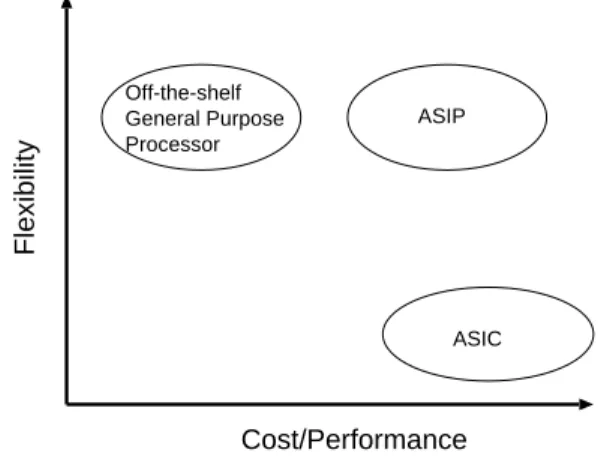
(2) No. 5. JPEG Encoder Design Space Exploration Using PEAS-III. sor specification language, because detail information is described when designers use these languages. The PEAS-III system 13)∼15) is one of the ASIP development systems, which generates not only synthesizable HDL descriptions but the target compiler and the target assembler. PEAS-III is based on processor specification language approach. Hence, wide range of processor architecture can be described using the PEAS-III system. The PEAS-III system has well parameterized resource models, Flexible Hardware Models (FHM) 16) . FHM-DBMS (DataBase Management System) produces the resource specification to generate HDL and the target compiler. When designers would like to change the features of resources, they only change the parameters of FHM. Moreover, designers describe processor specification through the PEAS-III input environment using GUIs. Resources and other architecture parameters are specified using GUIs. These features reduce the modification cost and improve design reuse. In this paper, JPEG encoder application, one of the typical DSP applications, was designed using the ASIP design methodology. Instructions for JPEG encoder, such as DCT instruction, and butterfly instructions, were added to the initial design. Area, performance, and execution cycles of processors were calculated using HDL descriptions, compiler, and assembler. From experimental results, various architectures can be designed in a short time, and designers can select an optimal architecture that matches design constraints. The rest of this paper is organized as follows. In Section 2, SoC design using ASIP is described. In Section 3, the PEAS-III system, one of the ASIP development systems, is introduced. The case study and experimental result are discussed in Section 4, and examined in Section 5. Finally, Section 6 concludes this paper and future work is described. 2. SoC Design Using ASIP Requirements of embedded systems such as consumer products, are cost effective architecture and low power. Moreover, rapid technology change makes product life cycles short and makes time-to-market a critical issue for industries. Time required for design and verification are measured in months or years with high uncertainly. One of the solutions for this requirement is ASIP (Application Specific. Flexibility. Vol. 44. Off-the-shelf General Purpose Processor. 1191. ASIP. ASIC. Cost/Performance Fig. 1 Advantage of ASIP solution.. Instruction-set Processor) solution. ASIP is a programmable processor that is designed for a specific, well-defined class of applications. An ASIP is usually characterized by a small, welldefined instruction-set that is tuned to the critical inner loops of the application code. Figure 1 shows advantage of ASIP solution. The horizontal axis is cost-performance ratio and the vertical axis is flexibility. Offthe-shelf general purpose processor like Intel Pentium processor has high flexibility, but cost-performance ratio of the general purpose processor is low. On the contrary, although ASIC achieves high cost-performance, ASIC has lower flexibility. The ASIP has higher flexibility than ASIC has, and achieves higher costperformance than the general purpose processor. Hence, ASIP can be one of the key component of SoCs. On the other hand, the cost of a SoC design is very expensive. Industry analysts make much of the rising cost of deep-submicron IC masks: The cost of a full mask set approaches $1 million. As a result, it is difficult that designers change the SoC specification and redevelop chips. ASIP design methods permit painless workarounds for the design cost problem because ASIP has flexibility. Hence, flexibility is a key issue in developing SoC. Although ASIC cannot satisfy flexibility, ASIP can satisfy flexibility. In addition, ASIP design methods increase designer productivity. RTL-based ASIC design routinely includes bugs because complexity of ASIC increases. An ASIP based SoC design method significantly cuts risks of fatal logic bugs and permits graceful recovery when testers discover a bug. The reason is that designers.
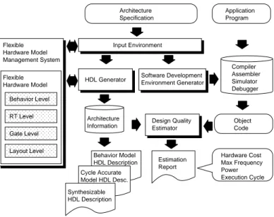
(3) 1192. IPSJ Journal Architecture Specification. Application Program. Input Environment. Flexible Hardware Model Management System Flexible Hardware Model. May 2003. HDL Generator. Software Development Environment Generator. Compiler Assembler Simulator Debugger. Behavior Level RT Level. Architecture Information. Design Quality Estimator. Object Code. Gate Level Layout Level. Behavior Model HDL Description. Estimation Report. Cycle Accurate Model HDL Desc.. Hardware Cost Max Frequency Power Execution Cycle. Synthesizable HDL Description. Fig. 2 Overview of PEAS-III system.. develop software instead of hardware logic in complex function fields. 3. ASIP Development System: PEASIII PEAS-III (Practical Environment for ASIP development) is one of the ASIP development systems. PEAS-III has the following features: (1) Synthesizable HDL description generation, (2) Software development environment generation, (3) Design reuse framework based on Flexible Hardware Model (FHM), and (4) Design quality estimation at early design phase. The overview of the PEAS-III system is shown in Fig. 2. Processor architecture specification is written in the input environment, which encourages efficient input. The processor specification description includes: (1) architecture parameters such as pipeline stage counts, the number of delayed branch slots, (2) declaration of resources included in the processor, such as ALUs and register files, (3) instruction format definitions, (4) behavior and microoperation descriptions of instructions, and (5) interrupt definitions including cause conditions and micro-operation description of interrupts. The architecture description is passed from the input environment to the HDL generator and the software development environment generator. The HDL generator and the compiler generator uses FHM, which is parameterized resource model. Since FHM is used in HDL and compiler generation, designers can change the characteristics of resource only by changing the. parameters of each resource. In the compiler generation method of PEASIII, special instructions can be added using Compiler-Known-Functions. Compiler-KnownFunctions directly replace instructions instead of constructing a usual function call. Designers can tune processors for the target application using Compiler-Known-Functions. It is the advantage of the PEAS-III design that a processor architect can design the synthesizable HDL and the target compiler rapidly. Since execution cycles, clock frequency and hardware cost can be evaluated in the early design phase, designers can find an optimal architecture in the short design time. 4. Case Study 4.1 Objective of Case Study Objective of this case study is to evaluate effectiveness of ASIP design method and the proposed ASIP development environment. Particularly, it is evaluated that design space exploration time using the PEAS-III system when designers develop an application system used in real world. Target applications of ASIP include digital signal processing (DSP) such as JPEG, MPEG, network system, wireless communication system such as mobile phone. JPEG is one of the target applications of ASIP, and JPEG is used for a lot of systems such as digital camera, mobile phone with camera, and so on. Hence, JPEG is a good example to confirm effectiveness of ASIP design method and the proposed ASIP development environment..
(4) Vol. 44. No. 5. JPEG Encoder Design Space Exploration Using PEAS-III. 1193. DCT based Encoder. 8 * 8 blocks. DCT. Quantization. VLC Compressed Image Data. Source Image Data. Table Specification. Table Specification. Fig. 3 JPEG encoder procedures based on the DCT. Step1. Step2 MADD3. x(0). x(7). C1_8 -S3_8. -1. x(3). x(6). MADD1 C1_4 C1_4. S1_8. x(2). x(5). Step4. X(0). C1_4 -C1_4. x(1). x(4). Step3. -1. X(4) X(2) MADD2 X(6). C3_8 S1_16. -1 -1 -1 -1 ADD2. -C1_4 C1_4 C1_4 C1_4. MADD1. S5_16. C1_16. C5_16 X(5). -1. -S3_16. -1 C3_16. ADD1. X(1). C7_16. X(3). -S7_16 X(7). MADD3. Fig. 4 Data flow of Chen DCT (1-dimensional 8 points).. 4.2 Target Application: JPEG Codec JPEG is a definition of a still-image compression algorithm established by the JPEG committee. Figure 3 shows JPEG encoder procedures based on the DCT. In the encoding process, the input component’s samples are grouped into 8 × 8 blocks, and each block is transformed by the DCT into a set of 64 values referred to as DCT coefficient. The first element is referred to as the DC coefficient and the other elements are referred to as the AC coefficients. Each of the 64 coefficients is then quantized using one of 64 corresponding values from a quantization table. After quantization, the DC coefficient and the 63 AC coefficients are prepared for Variable Length Coding (VLC) which compresses the DC and AC coefficients. In JPEG specification, one of two coding procedures can be used. One is Huffman encoding and the other is arithmetic coding. 4.3 Architecture Candidates Several kinds of parameters are defined in JPEG specification. In this case study, 8 bit. precision baseline algorithm was selected. Huffman coding was selected as VLC and VLD. In the following section, architecture candidates are described, and experimental results are explained. 4.3.1 DCT and IDCT DCT and IDCT are designed using Chen DCT algorithm 17) , which is one of the famous algorithm reducing multiplications and additions. Data flow of Chen DCT is shown in Fig. 4. Here, x(i) denotes element of input matrix, X(i) denotes transformed element. Ci j i×π and Si j denote cos( i×π j ) and sin( j ), respectively. Using Chen algorithm, multiplication times are reduced from 64 to 16, and addition times are reduced from 56 to 26 in 1 dimensional 8 points DCT. IDCT can be designed using inverse of DCT. Hence, multiplication and addition times in IDCT are reduced as much as those of DCT. There are several approaches in DCT and IDCT design..
(5) 1194. IPSJ Journal. • Sequential Instructions Approach Sequential instructions approach stands for software design. All of the algorithm is processed by software. • DCT Instruction Approach DCT instructions approach stands for hardware unit design. All of the algorithm is processed by hardware. • Butterfly Instructions Approach Butterfly instructions approach stands for design using fine grain instructions. The part of the algorithm is processed by hardware, and the other part of the algorithm is processed by software. These approaches have trade-offs between hardware cost and performance. 4.3.2 Quantization In quantization design, several approaches exist, which is the same as DCT design. Figure 5 shows the C source code of quantization.. May 2003. From Fig. 5, quantization divides the element by the element of quantization table. Hence, the performance of divider affects the execution cycles of quantization. In this case study, the algorithm of divider was changed. 4.4 Input Image In this evaluation, a standard image (Fig. 6) was used as an input image. The image size was 256×256 pixels and the sampling factors of each component were as follows: horizontal sampling factors of Y, U, V were 4, 1, 1, and vertical sampling factor were 4, 1, 1, respectively. 4.5 DCT/IDCT Unit Figure 7 shows the DCT/IDCT unit that processes 2 dimensional (2-D) 8 points DCT/IDCT. The input and output ports of DCT/IDCT unit consist of as follows: (a) input or output 32-bit data bus, (b) input port of 32-bit base address for data read/write, (c) 32-bit data address bus, (d) 1-bit calculation mode signal to change DCT execution or IDCT. quantization (short int ∗input, short int ∗output, short int ∗qtable) { short int *inputPtr = input; for ( ; inputPtr < input + 64; inputPtr++ ) { if ( ∗inputPtr > 0 ) { ∗output = (∗inputPtr + (∗qtable >> 1)) / ∗qtable; } else { ∗output = (∗inputPtr - (∗qtable >> 1)) / ∗qtable; } output++; qtable++; } }. Fig. 6 Sample color image (Lenna).. Fig. 5 C source code of quantization.. Read and Write base address. Data 2 data read/write or 1 data read/write on 32 bits data bass. Data address start. fin. address Unit selector. reg0. reg1. reg2. reg3. reg4. reg5. reg6. reg7. selector. ADD Block1. ADD Block2. MADD1. MADD2. Fig. 7 DCT/IDCT Unit.. MADD3. Controller.
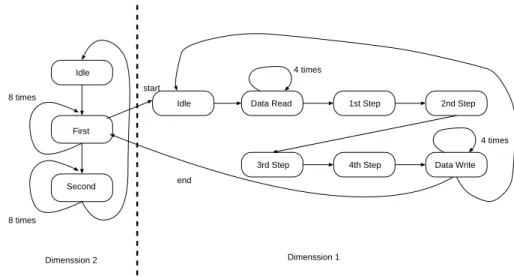
(6) Vol. 44. No. 5. JPEG Encoder Design Space Exploration Using PEAS-III. 1195. 4 times. Idle start 8 times. Idle. Data Read. 1st Step. 2nd Step. First 4 times 3rd Step Second. 4th Step. Data Write. end. 8 times. Dimenssion 2. Dimenssion 1. Fig. 8 Finite state machine of DCT/IDCT unit controller.. execution, (e) 1-bit start signal, and (f) 1bit fin signal. Functional blocks consist of 8 blocks: 16-bit internal registers, ADD block1, ADD block2, MADD1, MADD2, MADD3, address unit, and controller. ADD block1, ADD block2, MADD1, MADD2, and MADD3 execute part of Chen DCT data flow illustrated in Fig. 4. ADD block1 has 4 input ports (in1, in2, in3, in4), and 4 output ports (out1, out2, out3, out4). Each adder calculates using the following equation: out1 = in1 + in2, out2 = in1 − in2, out3 = −in3 + in4, out4 = in3 + in4. ADD block2 has 8 input ports (in1, in2, in3, in4, in5, in6, in7, in8), and 8 output ports (out1, out2, out3, out4, out5, out6, out7, out8). Each adder calculates using the following equation: out1 = in1 + in8, out2 = in2 + in7, out3 = in3 + in6, out4 = in4 + in5, out5 = in4 − in5, out6 = in3 − in6, out7 = in2 − in7, out8 = in1 − in8. MADD1 has 2 input ports (in1, in2) and 2 output ports (out1, out2). MADD1 unit calculates using the following equation: 1×π out1 = cos( 1×π 4 ) · in1 + cos( 4 ) · in2, out1 = 1×π 1×π cos( 4 ) · in1 − cos( 4 ) · in2. MADD2 has 2 input ports (in1, in2) and 2 output ports (out1, out2). MADD2 unit calculates using the follow1×π ing equation: out1 = sin( 1×π 8 ) · in1 + cos( 8 ) · 3×π 3×π in2, out2 = sin( 8 ) · in1 + cos( 8 ) · in2, MADD3 has 4 input ports (in1, in2, in3, in4) and 4 output ports (out1, out2, out3, out4). MADD3 unit can change calculation mode to use the same unit twice in Chen DCT/IDCT calculation flow. MADD3 unit calculates using the following equation: out1 = sin( 1×π 16 ) · in1 +. 5×π 5×π cos( 1×π 16 )·in4, out2 = sin( 16 )·in2+cos( 16 )· 3×π 3×π in3, out3 = − sin( 16 ) · in2 + cos( 16 ) · in3, 7×π out4 = − sin( 7×π 16 ) · in1 + cos( 16 ) · in4, or out1 = in1 + in4, out2 = in2 + in3, out3 = in2 − in3, out4 = in1 − in4. Each value is calculated in 16-bit fixed point arithmetic. Figure 8 shows the finite state machine of DCT/IDCT unit. The finite state machine consists of two part. One is 1-D Chen DCT calculation control part, the other is 2-D DCT calculation control part. In 2-D part, first step calculates row of matrix and second step calculates column of matrix. In each step, 1-D Chen DCT is executed 8 times. In 1-D part, the flow consists of data read, 4 steps execution illustrated in Fig. 4, and data write. The DCT/IDCT unit fetches data from the data memory to the internal registers. When the DCT/IDCT unit fetches data that is from row of matrix, one 16-bit value can be fetched using an address. In column data of matrix, two 16-bit values can be fetched using an address. Hence, the number of memory accesses when the DCT/IDCT unit fetches from row of matrix is 8, and the number of memory accesses when the DCT/IDCT unit fetches from column of matrix is 4. From this feature, the number of memory accesses can be reduced when the DCT/IDCT unit is used. The reason why the DCT/IDCT unit has 32-bit data bus is that the data is allocated to the data memory which is the same memory of ASIP..
(7) 1196. IPSJ Journal. May 2003. (a) Behavior Description for Compiler Generator. (a) Behavior Description for Compiler Generator. ckf prototype { void dct ( unsigned int , unsigned int ); }. }. DCT { operand { GPR UInt31to0 a; GPR UInt31to0 b; } format { “DCT” “,” a “,” b } function { stage(1) { PC.read IMEM.load word PC.inc IR.read } stage(2) {GPR.read0 GPR.read1 } stage(3) { } stage(4) { DCT0.dct } stage(5) { } } behavior { dct ( a , b ); } }. MADD1 { operand { GPR UInt15to0 a; GPR UInt15to0 b; } format { “MADD1” “,” a “,” b } function { stage(1) { PC.read IMEM.load word PC.inc IR.read } stage(2) {GPR.read0 GPR.read1 } stage(3) {MADD1U0.madd } stage(4) { } stage(5) {GPR.write0 GPR.write1 } } behavior { madd1 ( a , b ); } }. (b) Micro-Operation Description. (b) Micro-Operation Description. stage(1){ IR := IMEM[PC]; PC.inc();}, stage(2){ $op1 := GPR.read0(rs); $op2 := GPR.read1(rt);}, stage(3){}, stage(4){$dummy := DCT0.dct($op1,$op2);}, stage(5){}. stage(1){ IR := IMEM[PC]; PC.inc();}, stage(2){ $op1 := GPR.read0(rs); $op2 := GPR.read1(rt);}, stage(3){($result1, $result2) := MADD1U0.madd($op1, $op2);}, stage(4){ }, stage(5){GPR.write0($result1, rs); GPR.write1($result2, rt); }. (c) Bit Field 000000 rs. (c) Bit Field 000000 rs. rt. 0000000000. 111111. ckf prototype { void madd1 ( unsigned int , unsigned int );. Fig. 9 DCT instruction specification of PEAS-III.. 4.6 Additional Instructions • DCT DCT instruction executes the procedure of DCT. This instruction uses the DCT unit described in section 4.5. Instruction set specification for PEAS-III is described in Fig. 9. In application written in C language, DCT is described using function call. In PEAS-III specification, CompilerKnown-Function “dct” is defined, and the behavior of DCT instruction is defined using “dct” function. Micro-Operation description defines pipeline execution. DCT unit is executed at pipeline stage 4. • MADD1 MADD1 instruction calculates the MADD1 block in Fig. 4. MADD1 instruction takes 2 operands as input and write back to the same operand registers. Instruction set specification for PEAS-III is described in Fig. 10. In application written in C language, MADD1 is described using function call. In PEAS-III specification, CompilerKnown-Function “madd1” is defined, and the behavior of MADD1 instruction is defined using “madd1” function. MADD1 unit is executed at pipeline stage 3. • MADD2 MADD2 instruction calculates the MADD2 block in Fig. 4. MADD2 instruction takes 2 operands as input and write back to the same operand registers. Instruction set specification for PEAS-III is described in. rt. 0000000000. 011110. Fig. 10 MADD1 instruction specification of PEAS-III. (a) Behavior Description for Compiler Generator ckf prototype { void madd2 ( unsigned int , unsigned int ); } MADD2 { operand { GPR UInt15to0 a; GPR UInt15to0 b; } format { “MADD2” “,” a “,” b } function { stage(1) { PC.read IMEM.load word PC.inc IR.read } stage(2) {GPR.read0 GPR.read1 } stage(3) {MADD2U0.madd } stage(4) { } stage(5) {GPR.write0 GPR.write1} } behavior { madd2 ( a , b ); } } (b) Micro-Operation Description stage(1){ IR := IMEM[PC]; PC.inc();}, stage(2){ $op1 := GPR.read0(rs); $op2 := GPR.read1(rt);}, stage(3){($result1, $result2) := MADD2U0.madd($op1, $op2);}, stage(4){ }, stage(5){GPR.write0($result1, rs); GPR.write1($result2, rt);} (c) Bit Field 000000 rs. rt. 0000000000. 011111. Fig. 11 MADD2 instruction specification of PEAS-III.. Fig. 11. In application written in C language, MADD2 is described using function call. In PEAS-III specification, CompilerKnown-Function “madd2” is defined, and the behavior of MADD2 instruction is defined using “madd2” function. MADD2 unit is executed at pipeline stage 3. 4.7 Compiler Generation for Target Processors The target compiler is generated using pro-.
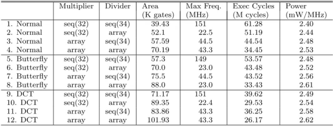
(8) Vol. 44. No. 5. JPEG Encoder Design Space Exploration Using PEAS-III. 1197. Table 1 Processor cores and their execution cycles of JPEG application.. 1. Normal 2. Normal 3. Normal 4. Normal 5. Butterfly 6. Butterfly 7. Butterfly 8. Butterfly 9. DCT 10. DCT 11. DCT 12. DCT. Multiplier. Divider. seq(32) seq(32) array array seq(32) seq(32) array array seq(32) seq(32) array array. seq(34) array seq(34) array seq(34) array seq(34) array seq(34) array seq(34) array. Area Max Freq. Exec Cycles Power (K gates) (MHz) (M cycles) (mW/MHz) 39.43 151 61.28 2.40 52.1 22.5 51.19 2.44 57.59 44.5 44.54 2.48 70.19 43.3 34.45 2.53 57.3 149 53.57 2.48 70.0 23.0 43.48 2.52 75.5 44.5 43.52 2.56 88.0 23.0 33.43 2.61 71.17 151 39.62 2.49 89.35 22.4 29.53 2.54 83.86 43.3 36.25 2.58 101.93 43.3 26.17 2.62 Library: 0.14 CMOS Standard Cell Library.. cessor specification partly represented in previous section. The target compiler produced by the proposed compiler generator executes the following steps: (1) Parsing the source code, (2) Machine independent optimization, (3) Syntax tree rewriting and pattern matching, (4) Register allocation and Spill code insertion, (5) Instruction scheduling, (6) Machine dependent optimization, and (7) Output assembly code. When special instructions such as DCT, MADD1 and so on are added to the processor specification, the proposed compiler generation method produces the following information: (a) function prototypes for C parser, (b) mapping rules for special instructions, and (c) instruction throughput and latency table for instruction scheduling. When parser reads the special instructions written in target application, the generated compiler makes CKF internal representation for compiler. When back-end of compiler generates assembler, target instruction is emitted using mapping rule for CKF. For example, DCT function is read by the compiler and the internal representation “xirCKF” is generated, which means that extended internal representation “CKF”. The “xirCKF” has attributes that include operands and CKF ID. The mapping rule for “xirCKF” specifies assembly format which is specified in format section. For instance, in DCT instruction in Fig. 9, the mapping rule of DCT instruction includes instruction string “DCT” and the operand order of DCT instruction “a” and “b”. Furthermore, instruction latency and throughput are calculated using resource usage described in function section of instruction behavior specification. Resource throughput and latency can be obtained from FHM-DBMS. The proposed compiler generator traces the resource connection graph and. calculates instruction throughput and latency. 4.8 How to Estimate Design Quality Hardware Cost and maximum clock frequency were estimated using Synopsys Design Compiler. Input of Design Compiler was synthesizable HDL generated by PEAS-III. 0.14 µm CMOS standard cell library (voltage 1.5 V) was used for logic synthesis. Execution cycle was estimated using Synopsys Scirocco that is a cycle-based HDL simulator. Dynamic power was estimated by gate-level simulation using Mentor Graphics ModelSim and Synopsys Power Compiler. 4.9 Processor Organization Processor organization in this case study is shown in Table 1. Normal denotes base instruction set that is sub set of MIPS-R3000 instruction set. Butterfly denotes instruction set added MADD1, and MADD2 instructions. DCT denotes instruction set added DCT instruction. The hardware algorithm of multiplier is sequential type that executes 32 cycles and array type that executes 1 cycle. On the other hand, the hardware algorithm of divider is sequential type that executes 34 cycles, and array type that executes 1 cycle. 4.10 Trade-offs Between Hardware Cost and Performance Figure 12 shows trade-offs between hardware cost and execution cycles when JPEG encoder has been executed. Horizontal axis is hardware cost, and vertical axis is execution cycles. The number of each plot point in Fig. 12 corresponds to each processor in Table 1. From Fig. 12, the trade-off between hardware cost and execution cycles exists when instructions are added and the hardware algorithms are changed. Figures 13 and 14 show trade-offs between.
(9) 1198. IPSJ Journal. May 2003. Fig. 12 Trade-offs between hardware cost and execution cycles when JPEG encoder was executed.. Fig. 15 Trade-offs between hardware cost and power consumption when JPEG encoder was executed within 0.5 second.. Fig. 13 Trade-offs between hardware cost and execution time when JPEG encoder was executed (66 MHz).. Fig. 16 Trade-offs between hardware cost and power consumption when JPEG encoder was executed within 1 second.. Fig. 14 Trade-offs between hardware cost and execution time when JPEG encoder was executed (40 MHz).. hardware cost and execution time when JPEG encoder has been executed. Horizontal axis is hardware cost, and vertical axis is execution time. In Fig. 13, execution time was calculated using execution cycles and clock frequency that was 66 MHz, and in Fig. 14, execution time was calculated using execution cycles and clock frequency that was 40 MHz. As shown in these figures, the number of architecture candidates was changed because the max clock frequency of each architecture candidate ranges between about 20 MHz and 150 MHz. These results. show that designers have to consider not only the execution cycles of an application, but also the clock frequency when architecture candidates are selected. In Fig. 13, when a design constraint is that hardware cost is under 60 K gates, the processor No.5 in Table 1 is selected as the optimal architecture. 4.11 Trade-offs Between Hardware Cost and Power Consumption Figures 15 and 16 show trade-offs between hardware cost and power consumption when JPEG encoder has been executed. The horizontal axis is hardware cost, and the vertical axis is dynamic power. In Fig. 15, JPEG Encoder was executed within 0.5 second, and in Fig. 16, JPEG Encoder was executed within 1 second. In Fig. 15, the frequency of processor 1 was about 120 MHz, the frequency of processor 9 was about 90 MHz. Hence, the dynamic power of processor 1 in Fig. 15 was about 290 mW, and the dynamic power of processor 9 was about 190 mW. If design constraint of power consumption is 200 mW, the processor 9 can be selected, but if design constraint of power consumption is 300 mW, processor 1 can be selected because the hardware cost of pro-.
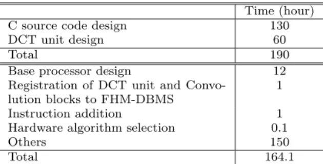
(10) Vol. 44. No. 5. JPEG Encoder Design Space Exploration Using PEAS-III. Table 2 Design time. C source code design DCT unit design Total Base processor design Registration of DCT unit and Convolution blocks to FHM-DBMS Instruction addition Hardware algorithm selection Others Total. Time (hour) 130 60 190 12 1 1 0.1 150 164.1. cessor 1 is smaller than that of processor 9. Furthermore, if design constraint of execution time is within 1 second, the trade-off between hardware cost and power consumption is Fig. 16. In Fig. 16, processors 5 and 7 cannot be architecture candidates. 4.12 Design Time The design time of the case study is shown in Table 2. From Table 2, about ten hours were spent using the PEAS-III system. Here, the reason why the hardware algorithm selection time is short is only changing FHM parameters to select hardware algorithm. From this result, the hardware description and the target compiler can be designed in a short design time. 130 hours were spent designing JPEG codec using C source code. 60 hours were spent DCT unit design. Others include debug time and simulation time and synthesizing time to evaluate the processor core. It seems that the time of JPEG codec application design and DCT unit design is as long as other environments. 5. Discussion The experimental result shows that architecture candidates are changed when clock frequency or time constraint are changed. From this result, designers must consider not only the execution cycles of a target processor but also the max frequency of a target processor and power consumption. For example, in Fig. 15, processor 5 can be an architecture candidate. However, in Fig. 16, processor 5 is not an architecture candidate because processor 3 can achieve low power and the same hardware cost. In the PEAS-III design, software development environment and designed processor’s HDL descriptions are generated at the same time. Hence, designers can consider the execution cycles of application, the clock frequency of processor, hardware cost and power consumption efficiently.. 1199. When an application such as DSP application is designed using ASIPs, designers consider trade-offs among hardware cost, performance and power consumption. Generally, it is said that the design time of hardware description, compiler and assembler require several months or at least several weeks. However, it is too long to meet a requirement of the design time in design space exploration. On the other hand, when designers use other ASIP development systems that have been explained in section 1, either software development environment or hardware description is produced in a short time, but the other part, for example processor cores for software development environment, must be developed by themselves. The advantage of the PEAS-III system is that compiler, assembler and hardware description are generated at the same time. Furthermore, the modification cost of the design is low, and hardware modules such as DCT unit can be reused easily, because designers only select modules from FHM-DBMS as resources. Using the PEAS-III system, designers can evaluate processors and select an optimal architecture in a short design time. The architecture candidates described in Section 4.3 were selected from the feature of C source code or data flow. Although a lot of candidates can be considered, several architecture candidates that were expected to improve processor performance were designed to evaluate the potential of PEAS-III design method in this case study. Generally, architecture candidates selection is very difficult. Hence, the profiling environment to select architecture candidates and architecture selection method are needed to reduce design cost and to get better solution. In Table 2, the time of others includes debug time and simulation time of target processor. To reduce this part, a source code debugger and a faster simulator are desirable. 6. Conclusion In this paper, JPEG encoder design space exploration using the PEAS-III system is described, which is one of the ASIP development system. Instructions for JPEG encoder, such as DCT instruction, and butterfly instructions, were added to the initial processor. Area, performance, and dynamic power of processors were calculated using the generated HDL description, compiler, and assembler. From experimental results, 12 architectures can be de-.
(11) 1200. IPSJ Journal. signed in a short time. Moreover, the design quality of each processor including hardware cost, execution cycles of application, clock frequency, and power consumption was evaluated using the PEAS-III system efficiently. Future work includes instruction set simulator, profiler, and debugger generation, and architecture candidates selection method. Acknowledgments The authors are grateful to the members of PEAS Project. The authors also would like to express thanks to Mr. Nobuyuki Hikichi from SRA (Software Research Associates Inc.). Moreover, the authors are also grateful to Japan Novel Corp. The compiler development kit CoSy is provided by ACE Associated Compiler Experts bv. This work was partly supported by STARC (Semiconductor Technology Academic Research Center), and one of tools was supported by Mentor Graphics higher education program. References 1) Sato, J., Alomary, A.Y., Honma, Y., Nakano, T., Shiomi, A., Hikichi, N. and Imai, M.: PEAS-I: A Hardware/Software Codesign System for ASIP Development, IEICE Trans. Fundamentals, Vol.E77-A, No.3, pp.483–491 (March 1994). 2) Shackleford, B., Yasuda, M., Okushi, E., Koizumi, H., Tomiyama, H. and Yasuura, H.: Satsuki: An Integrated Processor Synthesis and Compiler Generation System, IEICE Trans. Inf. & Syst., Vol.E79-D, No.10, pp.1373–1381 (Oct. 1996). 3) Yang, J.-H., Kim, B.-W., Nam, S.-J., Cho, J.H., Seo, S.-W., Ryu, C.-H., et al.: MetaCore: An Application Specific DSP Development System, 35th DAC, pp.800–803 (1998). 4) Campasano, R. and Wilberg, J.: Embedded System Design, Design Automation for Embedded Systems, Vol.1, No.1-2, pp.5–50 (Jan.1996). 5) Tensilica: Xtensa. http://www.tensilica.com 6) Fauth, A.: Beyond tool-specific machine descriptions, Code Generation for Embedded Processors, pp.138–152, Kluwer Academic Publishers (1995). 7) Hadjiyiannis, G., Russo, P. and Devadas, S.: A Methodology for Accurate Performance Evaluation in Architecture Exploration, 36th Design Automation Conference, pp.927–932 (June 1999). 8) Pees, S., Hoffmann, A., Zivojnovic, V. and Meyr, H.: LISA — Machine Description Language for Cycle-Accurate Models of Programmable DSP Architecture, 36th Design Automation Conference, pp.933–938 (1999).. May 2003. 9) Paulin, P.G., Liem, C., May, T.C. and Sutawala, S.: FlexWare: A Flexible Firmware Development Environment for Embedded Systems, Code Generation for Embedded Processors, pp.65–84 (1995). 10) Halambi, A., Grun, P., Ganesh, V., Khare, A., Dutt, N. and Nicolau, A.: EXPRESSION: A Language for Architecture Exploration through Compiler/Simulator Retargetability, DATE 99, pp.485–490 (March 1999). 11) Morimoto, T., Saito, K., Nakamura, H., Boku, T. and Nakazawa, K.: Advanced Processor Design Using Hardware Description Language AIDL, ASP-DAC’97, pp.387–390 (1997). 12) Hamabe, M., Nose, A., Togawa, N., Yanagisawa, M. and Ohtsuki, T.: A Generation System for Hardware Description of Pipelined Processors, Tech. Report of IEICE, VLD97-117, pp.33–40 (1997) (in japanese). 13) Itoh, M., Higaki, S., Sato, J., Shiomi, A., Takeuchi, Y., Kitajima, A. and Imai, M.: PEAS–III: An ASIP design environment, Proc. 2000 IEEE International Conference on Computer Design: VLSI in Computers & Processors (ICCD2000 ), pp.430–436 (Sept. 2000). 14) Kobayashi, S., Mita, K., Takeuchi, Y. and Imai, M.: Design Space Exploration for DSP Applications using the ASIP Development System PEAS-III, Proc. IEEE International Conference on Acoustics, Speech, and Signal Processing, Vol.3, pp.3168–3171 (May 2002). 15) Kobayashi, S., Takeuchi, Y., Kitajima, A. and Imai, M.: Compiler Generation in PEAS-III: an ASIP Development System, SCOPES 2001, St. Goal, Germany (March 2001). 16) Takeuchi, Y., Ueda, K., Yamane, Y., Shiomi, A. and Imai, M.: Flexible Hardware Model: A Hardware Model for IP Reuse and its Database Management System FHM-DBMS, Technical Report of IEICE, Vol.VLD2002-119, pp.221– 226 (Nov. 2002) (in japanese). 17) Chen, W.H., Smith, C.H. and Fralick, S.C.: A fast computational algorithm for the discrete cosine transform, IEEE Trans. Commun., Vol.COM-25, pp.1004–1009 (Sept. 1977).. (Received October 16, 2002) (Accepted March 4, 2003).
(12) Vol. 44. No. 5. JPEG Encoder Design Space Exploration Using PEAS-III. Shinsuke Kobayashi received his M.E. degree from Osaka University in 2000. He is currently a doctoral candidate in the Department of Informatics and Mathematical Sciences, Graduate School of Engineering Science at Osaka University. His research interests include software development environment generation for ASIPs, VLSI design, processor architecture and VLSI CAD. He is a member of IEEE CAS Society, ACM SIGDA, and IEICE. Kentaro Mita received his B.E. degree from Osaka University in 2001. He is currently a master’s candidate in the Department of Informatics and Mathematical Sciences, Graduate School of Engineering Science at Osaka University. His research interests include software development environment generation for ASIPs. Yoshinori Takeuchi received his B.E., M.E. and Dr. Eng. degrees from Tokyo Institute of Technology in 1987, 1989 and 1992, respectively. He is currently an Associate Professor of the Graduate School of Engineering Science at Osaka University. His research interests include digital signal processing, VLSI design and VLSI CAD. He is a member of IEEE of SP, CAS, and SSC Society, and IEICE.. 1201. Masaharu Imai received his B.S., M.S., and Ph.D. degrees from Nagoya University, Nagoya, Japan in 1974, 1976, and 1979, respectively. He joined the Department of Information and Computer Sciences at Toyohashi University of Technology in 1979. He was a visiting Assistant Professor at the University of South Carolina, SC, U.S.A. from 1984 to 1985. Since 1996, he has been with the Department of Informatics and Mathematical Science, Graduate School of Engineering Science, Osaka University, where he is currently a professor. Since 1991, he has been working for the Standardization of VHDL under IEEE/DASC and EIAJ (Electronic Industries Association of Japan). His research interests include HW/SW Codesign and VLSI architecture. He is a member of IEICE of Japan, IPSJ, IEEE, and ACM..
(13)
図


+5

関連したドキュメント
We can now state the fundamental theorem of model ∞-categories, which says that under the expected co/fibrancy hypotheses, the spaces of left and right homotopy classes of maps
By using the averaging theory of the first and second orders, we show that under any small cubic homogeneous perturbation, at most two limit cycles bifurcate from the period annulus
4 because evolutionary algorithms work with a population of solutions, various optimal solutions can be obtained, or many solutions can be obtained with values close to the
Several control schemes for the stability/synchronization/solution problem of nonlinear systems have been studied extensively, such as backstepping design 8, feedback control
Lamé’s formulas for the eigenvalues and eigenfunctions of the Laplacian on an equilateral triangle under Dirichlet and Neumann boundary conditions are herein extended to the
In order to be able to apply the Cartan–K¨ ahler theorem to prove existence of solutions in the real-analytic category, one needs a stronger result than Proposition 2.3; one needs
In order to predict the interior noise of the automobile in the low and middle frequency band in the design and development stage, the hybrid FE-SEA model of an automobile was
Henson, “Global dynamics of some periodically forced, monotone difference equations,” Journal of Di ff erence Equations and Applications, vol. Henson, “A periodically
