®
Altera Corporation 1
APEX 20K
Programmable Logic Device Family
March 2000, ver. 2.06 Data Sheet
Features...
■Industry’s first programmable logic device (PLD) incorporating system-on-a-programmable-chip integration
– MultiCore
TMarchitecture integrating look-up table (LUT) logic, product-term logic, and embedded memory
Preliminary Information
– LUT logic used for register-intensive functions
– Embedded system block (ESB) used to implement memory functions, including first-in first-out (FIFO) buffers, dual-port RAM, and content-addressable memory (CAM)
– ESB implementation of product-term logic used for combinatorial-intensive functions
■
High density
– 30,000 to 1.5 million typical gates (see Table 1) – Up to 51,840 logic elements (LEs)
– Up to 442,368 RAM bits that can be used without reducing available logic
– Up to 3,456 product-term-based macrocells
Note:
(1) The embedded IEEE Std. 1149.1 Joint Test Action Group (JTAG) boundary-scan circuitry contributes up to 57,000 additional gates.
Table 1. APEX 20K Device Features
Note (1)Feature EP20K30E EP20K60E EP20K100E EP20K100
EP20K160E EP20K200E EP20K200
EP20K300E EP20K400E EP20K400
EP20K600E EP20K1000E EP20K1500E
Maximum system gates
113,000 162,000 263,000 404,000 526,000 728,000 1,052,000 1,537,000 1,772,000 2,392,000
Typical gates
30,000 60,000 100,000 160,000 200,000 300,000 400,000 600,000 1,000,000 1,500,000
LEs 1,200 2,560 4,160 6,400 8,320 11,520 16,640 24,320 38,400 51,840
ESBs 12 16 26 40 52 72 104 152 160 216
Maximum RAM bits
24,576 32,768 53,248 81,920 106,496 147,456 212,992 311,296 327,680 442,368
Maximum macrocells
192 256 416 640 832 1,152 1,664 2,432 2,560 3,456
Maximum user I/O pins
128 204 252 316 382 408 502 624 708 808
2 Altera Corporation APEX 20K Programmable Logic Device Family Data Sheet Preliminary Information
...and More Features
■
Designed for low-power operation
– 1.8-V and 2.5-V supply voltage (see Table 2)
– MultiVolt
TMI/O interface support to interface with 1.8-V, 2.5-V, 3.3-V, and 5.0-Vdevices (see Table 2)
– ESB offering programmable power-saving mode
■
Flexible clock management circuitry with up to four phase-locked loops (PLL)
– Built-in low-skew clock tree – Up to eight global clock signals
– ClockLock
TMfeature reducing clock delay and skew – ClockBoost
TMfeature providing clock multiplication and
division
– ClockShift
TMprogrammable clock phase and delay shifting
■
Powerful I/O features
– Compliant with peripheral component interconnect Special Interest Group (PCI SIG)
PCI Local Bus Specification,Revision 2.2
for 3.3-V operation at 33 or 66 MHz and 32 or 64 bits – Support for high-speed external memories, including DDR
SDRAM and ZBT SRAM (ZBT is a trademark of Integrated Device Technology, Inc.)
– Bidirectional I/O performance (
tCO+
tSU) up to 370 MHz – LVDS performance up to 624 Mbits per channel
– Direct connection from I/O pins to local interconnect providing fast
tCOand
tSUtimes for complex logic
– MultiVolt I/O interface support to interface with 1.8-V, 2.5-V, 3.3-V, and 5.0-V devices (see Table 2)
– Programmable clamp to V
CCIO– Individual tri-state output enable control for each pin – Programmable output slew-rate control to reduce switching
noise
– Support for advanced I/O standards, including low-voltage differential signaling (LVDS), LVPECL, PCI-X, AGP, CTT, stub- series terminated logic (SSTL-3 and SSTL-2), and Gunning transceiver logic plus (GTL+) and high-speed terminated logic (HSTL Class I)
– Supports hot-socketing operation
– Pull-up on I/O pins before and during configuration
Preliminary Information APEX 20K Programmable Logic Device Family Data Sheet
Note:
(1) Certain APEX 20K devices are 5.0-V tolerant. See “MultiVolt I/O Interface” on page 46 for details.
■
Advanced interconnect structure
– Four-level hierarchical FastTrack
®Interconnect structure providing fast, predictable interconnect delays
– Dedicated carry chain that implements arithmetic functions such as fast adders, counters, and comparators (automatically used by software tools and megafunctions)
– Dedicated cascade chain that implements high-speed,
high-fan-in logic functions (automatically used by software tools and megafunctions)
– Interleaved local interconnect allows one LE to drive 29 other LEs through the fast local interconnect
■
Advanced packaging options
– Available in a variety of packages with 144 to 1,020 pins (see
Tables 3 through 6)– FineLine BGA
TMpackages maximize board space efficiency – SameFrame
TMpin migration providing migration capability
across device densities and package sizes
■
Advanced software support
– Software design support and automatic place-and-route provided by the Altera
®Quartus
TMdevelopment system for Windows-based PCs, Sun SPARCstations, and HP 9000 Series 700/800 workstations
– Altera MegaCore
TMfunctions and Altera Megafunction Partners Program (AMPP
SM) megafunctions
– NativeLink
TMintegration with popular synthesis, simulation, and timing analysis tools
Table 2. APEX 20K Supply Voltages
Feature EP20K100
EP20K200 EP20K400
EP20K60E EP20K100E EP20K160E EP20K200E EP20K300E EP20K400E EP20K600E EP20K1000E EP20K1500E
Internal supply voltage (VCCINT) 2.5 V 1.8 VMultiVolt I/O interface voltage levels (VCCIO)
2.5 V, 3.3 V 5.0 V (1)
1.8 V, 2.5 V, 3.3 V
4 Altera Corporation APEX 20K Programmable Logic Device Family Data Sheet Preliminary Information
– Quartus SignalTap
TMembedded logic analyzer simplifies in-system design evaluation by giving access to internal nodes during device operation
– Supports popular revision-control software packages including PVCS, RCS, and SCCS
Table 3. APEX 20K QFP, BGA & PGA Package Options & I/O Count
Notes (1), (2), (3)Device 144-Pin
TQFP
208-Pin PQFP RQFP
240-Pin PQFP RQFP
356-Pin BGA
652-Pin BGA
655-Pin PGA
984-Pin PGA
EP20K30E 92 128
EP20K60E 92 151 183 204
EP20K100 101 159 189 252
EP20K100E 92 151 183 246
EP20K160E 87 143 175 273
EP20K200 144 174 279
EP20K200E 136 168 273 376
EP20K300E 120 152 408
EP20K400 502 502
EP20K400E 488
EP20K600E 488
EP20K1000E 488 716
EP20K1500E 488 858
Table 4. APEX 20K FineLine BGA Package Options & I/O Count
Notes (1), (2), (3)Device 144 Pin 324 Pin 484 Pin 672 Pin 1,020 Pin
EP20K30E 108 128 128 (4) 128 (4)
EP20K60E 108 204 204 (4) 204 (4)
EP20K100 252 252 (4) 252 (4)
EP20K100E 108 246 246 (4) 246 (4)
EP20K160E 324 324 (4)
EP20K200 382 382 (4)
EP20K200E 376 376
EP20K300E 408
EP20K400 502 (5)
EP20K400E 488 (5)
EP20K600E 508 (5) 588
EP20K1000E 508 (5) 708
EP20K1500E 808
Preliminary Information APEX 20K Programmable Logic Device Family Data Sheet
Notes to tables:
(1) Contact Altera for up-to-date information on package availability.
(2) I/O counts include dedicated input and clock pins.
(3) APEX 20K device package types include thin quad flat pack (TQFP), plastic quad flat pack (PQFP), power quad flat pack (RQFP), 1.27-mm pitch ball-grid array (BGA), 1.00-mm pitch FineLine BGA, and pin-grid array (PGA) packages.
(4) All FineLine BGA packages, except the 144-pin and 1,020-pin packages, are footprint-compatible via SameFrame pin-out. Therefore, designers can design a board to support a variety of devices, providing a flexible migration path across densities and pin counts. Device migration is fully supported by Altera development tools. See “SameFrame Pin-Outs” on page 45 for more information.
(5) This device uses a thermally enhanced package, which is taller than the regular package. Consult the Altera Device Package Information Data Sheet for detailed package size information.
General Description
APEX 20K devices are the first PLDs designed with the MultiCore architecture, which combines the strengths of LUT-based and product- term-based devices with an enhanced memory structure. LUT-based logic provides optimized performance and efficiency for data-path, register- intensive, mathematical, or digital signal processing (DSP) designs.
Product-term-based logic is optimized for complex combinatorial paths, such as complex state machines. LUT- and product-term-based logic combined with memory functions and a wide variety of MegaCore and AMPP functions make the APEX 20K architecture uniquely suited for system-on-a-programmable-chip designs. Applications historically requiring a combination of LUT-, product-term-, and memory-based devices can now be integrated into one APEX 20K device.
Table 5. APEX 20K QFP, BGA & PGA Package Sizes
Feature 144-Pin TQFP 208-Pin QFP 240-Pin QFP 356-Pin BGA 652-Pin BGA 655-Pin PGA
Pitch (mm) 0.50 0.50 0.50 1.27 1.27 –
Area (mm2) 484 924 1,218 1,225 2,025 3,906
Length × Width (mm × mm)
22 × 22 30.4 × 30.4 34.9 × 34.9 35 × 35 45 × 45 62.5 × 62.5
Table 6. APEX 20K FineLine BGA Package Sizes
Feature 144 Pin 324 Pin 484 Pin 672 Pin 1,020 Pin
Pitch (mm) 1.00 1.00 1.00 1.00 1.00
Area (mm2) 169 361 529 729 1,089
Length × Width (mm × mm) 13 × 13 19 × 19 23 × 23 27 × 27 33 × 33
6 Altera Corporation APEX 20K Programmable Logic Device Family Data Sheet Preliminary Information
APEX 20KE devices are a superset of APEX 20K devices and include additional features such as advanced I/O standard support, CAM, additional global clocks, and enhanced ClockLock clock circuitry. In addition, APEX 20KE devices extend the APEX 20K family to over one million gates. APEX 20KE devices are denoted with an “E” suffix in the device name (e.g., the EP20K1000E device is an APEX 20KE device).
Table 7 summarizes the features included in APEX 20K and APEX 20KE
devices.
Preliminary Information APEX 20K Programmable Logic Device Family Data Sheet
Table 7. Comparison of APEX 20K & APEX 20KE Features
Feature APEX 20K Devices APEX 20KE Devices
MultiCore system integration Full support Full support Hot-socketing support Full support Full support SignalTap logic analysis Full support Full support 64-Bit, 66-MHz PCI Full compliance Full compliance MultiVolt I/O 2.5-V or 3.3-V VCCIO
VCCIO selected for device
1.8-V, 2.5-V, or 3.3-V VCCIO VCCIO selected block-by-block ClockLock support Clock delay reduction
2× and 4× clock multiplication
Clock delay reduction m/(n×v) clock multiplication Drive ClockLock output off-chip External clock feedback ClockShift
LVDS support Up to four PLLs
ClockShift, clock phase adjustment
Dedicated clock and input pins Six Eight
I/O standard support 2.5-V, 3.3-V, 5.0-V I/O 3.3-V PCI
Low-voltage complementary metal-oxide semiconductor (LVCMOS)
Low-voltage transistor-to-transistor logic (LVTTL)
1.8-V, 2.5-V, 3.3-V I/O 2.5-V I/O
3.3-V PCI and PCI-X
3.3-V Advanced Graphics Port (AGP) Center tap terminated (CTT)
GTL+
LVCMOS
LVDS and LVPELL data pins (in EP20K300E and larger devices) LVDS and LVPELL clock pins (in all devices)
LVTTL HSTL Class I LVPECL PCI-X
SSTL-2 Class I and II SSTL-3 Class I and II Memory support Dual-port RAM
FIFO RAM ROM
CAM
Dual-port RAM FIFO
RAM ROM
8 Altera Corporation APEX 20K Programmable Logic Device Family Data Sheet Preliminary Information
All APEX 20K devices are reconfigurable and are 100
%tested prior to shipment. As a result, test vectors do not have to be generated for fault coverage purposes. Instead, the designer can focus on simulation and design verification. In addition, the designer does not need to manage inventories of different application-specific integrated circuit (ASIC) designs; APEX 20K devices can be configured on the board for the specific functionality required.
APEX 20K devices are configured at system power-up with data stored in an Altera serial configuration device or provided by a system controller.
Altera offers in-system programmability (ISP)-capable EPC1
configuration devices, which configure APEX 20K devices via a serial data stream. Moreover, APEX 20K devices contain an optimized interface that permits microprocessors to configure APEX 20K devices serially or in parallel, and synchronously or asynchronously. The interface also enables microprocessors to treat APEX 20K devices as memory and configure the device by writing to a virtual memory location, making reconfiguration easy.
1
Contact Altera for information on future configuration devices.
After an APEX 20K device has been configured, it can be reconfigured in-circuit by resetting the device and loading new data. Real-time changes can be made during system operation, enabling innovative reconfigurable computing applications.
APEX 20K devices are supported by Altera’s Quartus development system, a single, integrated package that offers HDL and schematic design entry, compilation and logic synthesis, full simulation and worst-case timing analysis, SignalTap logic analysis, and device configuration. The Quartus software runs on Windows-based PCs, Sun SPARCstations, and HP 9000 Series 700/800 workstations.
The Quartus software provides NativeLink interfaces to other industry-
standard PC- and UNIX workstation-based EDA tools. For example,
designers can invoke the Quartus software from within third-party design
tools. Further, the Quartus software contains built-in optimized synthesis
libraries; synthesis tools can use these libraries to optimize designs for
APEX 20K devices. For example, the Synopsys Design Compiler library,
supplied with the Quartus development system, includes DesignWare
functions optimized for the APEX 20K architecture.
Preliminary Information APEX 20K Programmable Logic Device Family Data Sheet
Functional Description
APEX 20K devices incorporate LUT-based logic, product-term-based logic, and memory into one device. Signal interconnections within APEX 20K devices (as well as to and from device pins) are provided by the FastTrack Interconnect—a series of fast, continuous row and column channels that run the entire length and width of the device.
Each I/O pin is fed by an I/O element (IOE) located at the end of each row and column of the FastTrack Interconnect. Each IOE contains a
bidirectional I/O buffer and a register that can be used as either an input or output register to feed input, output, or bidirectional signals. When used with a dedicated clock pin, these registers provide exceptional performance. IOEs provide a variety of features, such as 3.3-V, 64-bit, 66-MHz PCI compliance; JTAG BST support; slew-rate control; and tri-state buffers. APEX 20KE devices offer enhanced I/O support, including support for 1.8-V I/O, 2.5-V I/O, LVCMOS, LVTTL, HSTL, LVPECL, 3.3-V PCI, PCI-X, LVDS, LVPELL GTL+, SSTL-2, SSTL-3, HSTL, CTT, and 3.3-V AGP I/O standards.
The ESB can implement a variety of memory functions, including CAM, RAM, dual-port RAM, ROM, and FIFO functions. Embedding the memory directly into the die improves performance and reduces die area compared to distributed-RAM implementations. Moreover, the
abundance of cascadable ESBs ensures that the APEX 20K device can implement multiple wide memory blocks for high-density designs. The ESB’s high speed ensures it can implement small memory blocks without any speed penalty. The abundance of ESBs ensures that designers can create as many different-sized memory blocks as the system requires.
Figure 1 shows an overview of the APEX 20K device.
Figure 1. APEX 20K Device Block Diagram
LUT
LUT LUT LUT
LUT
Memory
Memory Memory
Memory
IOE IOE
IOE IOE
IOE
IOE
IOE IOE
LUT
LUT Memory
Memory IOE
IOE Product Term
Product Term LUT
LUT Memory
Memory IOE
IOE Product Term
Product Term Product Term
Product Term Product Term
Product Term
FastTrack Interconnect Clock Management Circuitry
IOEs support PCI, GTL+, SSTL-3, LVDS, and other standards.
ClockLock
Four-input LUT for data path and DSP functions.
Product-term integration for high-speed control logic and state machines.
Flexible integration of embedded memory, including CAM, RAM, ROM, FIFO, and other memory functions.
10 Altera Corporation APEX 20K Programmable Logic Device Family Data Sheet Preliminary Information
APEX 20K devices provide two dedicated clock pins and four dedicated input pins that drive register control inputs. These signals ensure efficient distribution of high-speed, low-skew control signals. These signals use dedicated routing channels to provide short delays and low skews. Four of the dedicated inputs drive four global signals. These four global signals can also be driven by internal logic, providing an ideal solution for a clock divider or internally generated asynchronous clear signals with high fan-out. The dedicated clock pins featured on the APEX 20K devices can also feed logic. The devices also feature ClockLock and ClockBoost clock management circuitry. APEX 20KE devices provide two additional dedicated clock pins, for a total of four dedicated clock pins.
MegaLAB Structure
APEX 20K devices are constructed from a series of MegaLAB
TMstructures. Each MegaLAB structure contains 16 logic array blocks (LABs), one ESB, and a MegaLAB interconnect, which routes signals within the MegaLAB structure. In EP20K1000E and EP20K1500E devices, MegaLAB structures contain 24 LABs. Signals are routed between MegaLAB structures and I/O pins via the FastTrack Interconnect. In addition, edge LABs can be driven by I/O pins through the local interconnect. Figure 2 shows the MegaLAB structure.
Figure 2. MegaLAB Structure
ESB MegaLAB Interconnect
Local Interconnect To Adjacent
LAB or IOEs
LABs LE1
LE2 LE3 LE4 LE5 LE6 LE7 LE8 LE9 LE10
LE1 LE2 LE3 LE4 LE5 LE6 LE7 LE8 LE9 LE10
LE1 LE2 LE3 LE4 LE5 LE6 LE7 LE8 LE9 LE10
Preliminary Information APEX 20K Programmable Logic Device Family Data Sheet
Logic Array Block
Each LAB consists of 10 LEs, the LEs’ associated carry and cascade chains, LAB control signals, and the local interconnect. The local interconnect transfers signals between LEs in the same or adjacent LABs, IOEs, or ESBs.
The Quartus Compiler places associated logic within an LAB or adjacent LABs, allowing the use of a fast local interconnect for high performance.
Figure 3 shows the APEX 20K LAB.
APEX 20K devices use an interleaved LAB structure. This structure allows each LE to drive two local interconnect areas. This feature minimizes use of the MegaLAB and FastTrack interconnect, providing higher
performance and flexibility. Each LE can drive 29 other LEs through the fast local interconnect.
Figure 3. LAB Structure
To/From Adjacent LAB, ESB, or IOEs To/From
Adjacent LAB, ESB, or IOEs
The 10 LEs in the LAB are driven by two local interconnect areas. These LEs can drive two local interconnect areas.
Local Interconnect LEs drive local
MegaLAB, row, and column interconnects.
Column Interconnect Row
Interconnect
MegaLAB Interconnect
12 Altera Corporation
Each LAB contains dedicated logic for driving control signals to its LEs and ESBs. The control signals include clock, clock enable, asynchronous clear, asynchronous preset, asynchronous load, synchronous clear, and synchronous load signals. A maximum of six control signals can be used at a time. Although synchronous load and clear signals are generally used when implementing counters, they can also be used with other functions.
Each LAB can use two clocks and two clock enable signals. Each LAB’s clock and clock enable signals are linked (e.g., any LE in a particular LAB using
CLK1will also use
CLKENA1). LEs with the same clock but different clock enable signals either use both clock signals in one LAB or are placed into separate LABs.
If both the rising and falling edges of a clock are used in an LAB, both LAB-wide clock signals are used.
The LAB-wide control signals can be generated from the LAB local interconnect, global signals, and dedicated clock pins. The inherent low skew of the FastTrack Interconnect enables it to be used for clock distribution. Figure 4 shows the LAB control signal generation circuit.
Figure 4. LAB Control Signal Generation
Notes:
(1) APEX 20KE devices have four dedicated clocks.
(2) The LABCLR1 and LABCLR2 signals also control asynchronous load and asynchronous preset for LEs within the LAB.
(3) The SYNCCLR signal can be generated by the local interconnect or global signals.
SYNCCLR or LABCLK2 (3)
SYNCLOAD or LABCLKENA2
LABCLK1
LABCLKENA1
LABCLR2 (2)
LABCLR1 (2) Dedicated
Clocks Global Signals Local
Interconnect Local Interconnect Local Interconnect Local Interconnect
2 or 4 (1) 4
Logic Element
The LE, the smallest unit of logic in the APEX 20K architecture, is compact and provides efficient logic usage. Each LE contains a four-input LUT, which is a function generator that can quickly implement any function of four variables. In addition, each LE contains a programmable register and carry and cascade chains. Each LE drives the local interconnect, MegaLAB interconnect, and FastTrack Interconnect routing structures. See Figure 5.
Figure 5. APEX 20K Logic Element
Each LE’s programmable register can be configured for D, T, JK, or SR operation. The register’s clock and clear control signals can be driven by global signals, general-purpose I/O pins, or any internal logic. For combinatorial functions, the register is bypassed and the output of the LUT drives the outputs of the LE.
labclk1 labclk2 labclr1 labclr2
Carry-In
Clock &
Clock Enable Select
Carry-Out Look-Up
Table (LUT)
Carry Chain
Cascade Chain Cascade-In
Cascade-Out
To F astTrack Interconnect, MegaLAB Interconnect, or Local Interconnect
To F astTrack Interconnect, MegaLAB Interconnect, or Local Interconnect Programmable
Register
PRN
CLRN
D Q
ENA
Register Bypass
Packed Register Select
Chip-Wide Reset
labclkena1 labclkena2
Synchronous Load & Clear
Logic LAB-wide Synchronous
Load
LAB-wide Synchronous
Clear
Asynchronous Clear/Preset/
Load Logic data1
data2 data3 data4
14 Altera Corporation
Each LE has two outputs that drive the local, MegaLAB, or FastTrack Interconnect routing structure. Each output can be driven independently by the LUT’s or register’s output. For example, the LUT can drive one output while the register drives the other output. This feature, called register packing, improves device utilization because the register and the LUT can be used for unrelated functions. The LE can also drive out registered and unregistered versions of the LUT output.
The APEX 20K architecture provides two types of dedicated high-speed data paths that connect adjacent LEs without using local interconnect paths: carry chains and cascade chains. A carry chain supports high-speed arithmetic functions such as counters and adders, while a cascade chain implements wide-input functions such as equality comparators with minimum delay. Carry and cascade chains connect LEs 1 through 10 in an LAB and all LABs in the same MegaLAB structure.
Carry Chain
The carry chain provides a very fast carry-forward function between LEs.
The carry-in signal from a lower-order bit drives forward into the higher- order bit via the carry chain, and feeds into both the LUT and the next portion of the carry chain. This feature allows the APEX 20K architecture to implement high-speed counters, adders, and comparators of arbitrary width. Carry chain logic can be created automatically by the Quartus Compiler during design processing, or manually by the designer during design entry. Parameterized functions such as library of parameterized modules (LPM) and DesignWare functions automatically take advantage of carry chains for the appropriate functions.
The Quartus Compiler creates carry chains longer than ten LEs by linking LABs together automatically. For enhanced fitting, a long carry chain skips alternate LABs in a MegaLAB structure. A carry chain longer than one LAB skips either from an even-numbered LAB to the next even- numbered LAB, or from an odd-numbered LAB to the next odd-
numbered LAB. For example, the last LE of the first LAB in the upper-left MegaLAB structure carries to the first LE of the third LAB in the
MegaLAB structure.
Figure 6 shows how an n-bit full adder can be implemented in n + 1 LEs
with the carry chain. One portion of the LUT generates the sum of two bits
using the input signals and the carry-in signal; the sum is routed to the
output of the LE. The register can be bypassed for simple adders or used
for accumulator functions. Another portion of the LUT and the carry
chain logic generates the carry-out signal, which is routed directly to the
carry-in signal of the next-higher-order bit. The final carry-out signal is
routed to an LE, where it is driven onto the local, MegaLAB, or FastTrack
Interconnect routing structures.
Figure 6. APEX 20K Carry Chain
a1 LUT b1
Carry Chain
s1
LE1 Register
a2 b2
Carry Chain
s2
LE2 Register
Carry Chain
sn
LEn Register an
bn
Carry Chain
Carry-Out
LEn + 1 Register Carry-In
LUT
LUT
LUT
16 Altera Corporation
Cascade Chain
With the cascade chain, the APEX 20K architecture can implement functions with a very wide fan-in. Adjacent LUTs can compute portions of a function in parallel; the cascade chain serially connects the
intermediate values. The cascade chain can use a logical
ANDor logical
OR(via De Morgan’s inversion) to connect the outputs of adjacent LEs. Each additional LE provides four more inputs to the effective width of a function, with a short cascade delay. Cascade chain logic can be created automatically by the Quartus Compiler during design processing, or manually by the designer during design entry.
Cascade chains longer than ten LEs are implemented automatically by linking LABs together. For enhanced fitting, a long cascade chain skips alternate LABs in a MegaLAB structure. A cascade chain longer than one LAB skips either from an even-numbered LAB to the next even-numbered LAB, or from an odd-numbered LAB to the next odd-numbered LAB. For example, the last LE of the first LAB in the upper-left MegaLAB structure carries to the first LE of the third LAB in the MegaLAB structure. Figure 7 shows how the cascade function can connect adjacent LEs to form functions with a wide fan-in.
Figure 7. APEX 20K Cascade Chain
LE1 LUT
LE2 LUT
d[3..0]
d[7..4]
d[(4n – 1)..(4n – 4)]
d[3..0]
d[7..4]
LEn
LE1
LE2
LEn LUT
LUT
LUT
LUT
AND Cascade Chain OR Cascade Chain
d[(4n – 1)..(4n – 4)]
LE Operating Modes
The APEX 20K LE can operate in one of the following three modes:
■
Normal mode
■
Arithmetic mode
■
Counter mode
Each mode uses LE resources differently. In each mode, seven available inputs to the LE—the four data inputs from the LAB local interconnect, the feedback from the programmable register, and the carry-in and cascade-in from the previous LE—are directed to different destinations to implement the desired logic function. LAB-wide signals provide clock, asynchronous clear, asynchronous preset, asynchronous load,
synchronous clear, synchronous load, and clock enable control for the register. These LAB-wide signals are available in all LE modes.
The Quartus software, in conjunction with parameterized functions such as LPM and DesignWare functions, automatically chooses the
appropriate mode for common functions such as counters, adders, and
multipliers. If required, the designer can also create special-purpose
functions that specify which LE operating mode to use for optimal
performance. Figure 8 shows the LE operating modes.
18 Altera Corporation
Figure 8. APEX 20K LE Operating Modes
Notes:
(1) LEs in normal mode support register packing.
(2) There are two LAB-wide clock enables per LAB.
(3) When using the carry-in in normal mode, the packed register feature is unavailable.
(4) A register feedback multiplexer is available on LE1 of each LAB.
(5) The DATA1 and DATA2 input signals can supply counter enable, up or down control, or register feedback signals for LEs other than the second LE in an LAB.
(6) The LAB-wide synchronous clear and LAB wide synchronous load affect all registers in an LAB.
PRN
CLRN
D Q
4-Input LUT Carry-In (3)
Cascade-Out Cascade-In
LE-Out Normal Mode (1)
PRN
CLRN
D Q
Cascade-Out Cascade-In
3-Input LUT Carry-In
3-Input LUT
Carry-Out Arithmetic Mode
Counter Mode
data1 (5)
data2 (5) PRN
CLRN
D Q
Carry-In
LUT
3-Input 3-Input
LUT
Carry-Out data3 (data)
Cascade-Out Cascade-In
LAB-Wide Synchronous Load (6)
LAB-Wide Synchronous Clear (6)
(4)
LE-Out
LE-Out
LE-Out
LE-Out
LE-Out ENA
LAB-Wide Clock Enable (2)
ENA LAB-Wide Clock Enable (2)
ENA LAB-Wide Clock Enable (2)
data1 data2
data1 data2 data3 data4
Normal Mode
The normal mode is suitable for general logic applications, combinatorial functions, or wide decoding functions that can take advantage of a cascade chain. In normal mode, four data inputs from the LAB local interconnect and the carry-in are inputs to a four-input LUT. The Quartus Compiler automatically selects the carry-in or the
DATA3signal as one of the inputs to the LUT. The LUT output can be combined with the cascade-in signal to form a cascade chain through the cascade-out signal.
LEs in normal mode support packed registers.
Arithmetic Mode
The arithmetic mode is ideal for implementing adders, accumulators, and comparators. An LE in arithmetic mode uses two 3-input LUTs. One LUT computes a three-input function; the other generates a carry output. As shown in Figure 8, the first LUT uses the carry-in signal and two data inputs from the LAB local interconnect to generate a combinatorial or registered output. For example, when implementing an adder, this output is the sum of three signals:
DATA1,
DATA2, and carry-in. The second LUT uses the same three signals to generate a carry-out signal, thereby creating a carry chain. The arithmetic mode also supports simultaneous use of the cascade chain. LEs in arithmetic mode can drive out registered and unregistered versions of the LUT output.
The Quartus software implements parameterized functions that use the arithmetic mode automatically where appropriate; the designer does not need to specify how the carry chain will be used.
Counter Mode
The counter mode offers clock enable, counter enable, synchronous
up/down control, synchronous clear, and synchronous load options. The
counter enable and synchronous up/down control signals are generated
from the data inputs of the LAB local interconnect. The synchronous clear
and synchronous load options are LAB-wide signals that affect all
registers in the LAB. Consequently, if any of the LEs in an LAB use the
counter mode, other LEs in that LAB must be used as part of the same
counter or be used for a combinatorial function. The Quartus software
automatically places any registers that are not used by the counter into
other LABs.
20 Altera Corporation
The counter mode uses two three-input LUTs: one generates the counter data, and the other generates the fast carry bit. A 2-to-1 multiplexer provides synchronous loading, and another
ANDgate provides
synchronous clearing. If the cascade function is used by an LE in counter mode, the synchronous clear or load overrides any signal carried on the cascade chain. The synchronous clear overrides the synchronous load.
LEs in arithmetic mode can drive out registered and unregistered versions of the LUT output.
Clear & Preset Logic Control
Logic for the register’s clear and preset signals is controlled by LAB-wide signals. The LE directly supports an asynchronous clear function. The Quartus Compiler can use a
NOT-gate push-back technique to emulate an asynchronous preset. Moreover, the Quartus Compiler can use a
programmable
NOT-gate push-back technique to emulate simultaneous preset and clear or asynchronous load. However, this technique uses three additional LEs per register. All emulation is performed automatically when the design is compiled. Registers that emulate simultaneous preset and load will enter an unknown state upon power-up or when the chip- wide reset is asserted.
In addition to the two clear and preset modes, APEX 20K devices provide a chip-wide reset pin (
DEV_CLRn) that resets all registers in the device.
Use of this pin is controlled through an option in the Quartus software that is set before compilation. The chip-wide reset overrides all other control signals. Registers using an asynchronous preset are preset when the chip-wide reset is asserted; this effect results from the inversion technique used to implement the asynchronous preset.
FastTrack Interconnect
In the APEX 20K architecture, connections between LEs, ESBs, and I/O pins are provided by the FastTrack Interconnect. The FastTrack
Interconnect is a series of continuous horizontal and vertical routing channels that traverse the device. This global routing structure provides predictable performance, even in complex designs. In contrast, the segmented routing in FPGAs requires switch matrices to connect a variable number of routing paths, increasing the delays between logic resources and reducing performance.
The FastTrack Interconnect consists of row and column interconnect
channels that span the entire device. The row interconnect routes signals
throughout a row of MegaLAB structures; the column interconnect routes
signals throughout a column of MegaLAB structures. When using the row
and column interconnect, an LE, IOE, or ESB can drive any other LE, IOE,
or ESB in a device. See Figure 9.
Figure 9. APEX 20K Interconnect Structure
A row line can be driven directly by LEs, IOEs, or ESBs in that row.
Further, a column line can drive a row line, allowing an LE, IOE, or ESB to drive elements in a different row via the column and row interconnect.
The row interconnect drives the MegaLAB interconnect to drive LEs, IOEs, or ESBs in a particular MegaLAB structure.
A column line can be directly driven by LEs, IOEs, or ESBs in that column.
A column line on a device’s left or right edge can also be driven by row IOEs. The column line is used to route signals from one row to another. A column line can drive a row line; it can also drive the MegaLAB
interconnect directly, allowing faster connections between rows.
Figure 10 shows how the FastTrack Interconnect uses the local
interconnect to drive LEs within MegaLAB structures.
MegaLAB MegaLAB MegaLAB MegaLAB I/O
I/O I/O I/O I/O
I/O I/O
I/O
MegaLAB MegaLAB MegaLAB MegaLAB I/O
MegaLAB MegaLAB MegaLAB MegaLAB I/O
I/O I/O I/O I/O
Column Interconnect Column
Interconnect Row Interconnect
22 Altera Corporation
Figure 10. FastTrack Connection to Local Interconnect
L A B
L A B L A B
L A B E S B
L A B L A B I/O
I/O
MegaLAB Column
Row
MegaLAB
MegaLAB Interconnect
Row & Column Interconnect Drives MegaLAB Interconnect
MegaLAB Interconnect Drives Local Interconnect
L A B
L A B
E S B Row
Column E
S B
L A B
Figure 11 shows the intersection of a row and column interconnect, and
how these forms of interconnects and LEs drive each other.
Figure 11. Driving the FastTrack Interconnect
APEX 20KE devices include an enhanced interconnect structure for faster routing of input signals with high fan-out. Column I/O pins can drive the FastRow interconnect, which routes signals directly into the local interconnect without having to drive through the MegaLAB interconnect.
FastRow lines traverse two MegaLAB structures. Also, these pins can drive the local interconnect directly for fast setup times. On EP20K300E and larger devices, the FastRow interconnect drives the two MegaLABs in the top left corner and the two MegaLABs in the bottom right corner. On EP20K200E and smaller devices, FastRow interconnect drives the two MegaLABs on the top and the two MegaLABs on the bottom of the device.
On all devices, the FastRow interconnect drives all local interconnect in the appropriate MegaLABs except the interconnect areas on the far left and far right of the MegaLAB. Figure 12 shows the FastRow interconnect.
Row Interconnect
MegaLAB Interconnect
LE
Column Interconnect
Local Interconnect
24 Altera Corporation
Figure 12. APEX 20KE FastRow Interconnect
Table 8 summarizes how various elements of the APEX 20K architecture
drive each other.
IOE IOE FastRow Interconnect IOE IOE
Drives Local Interconnect in Two MegaLAB Structures
MegaLAB MegaLAB
Local Interconnect Select Vertical I/O Pins Drive Local Interconnect and FastRow Interconnect FastRow
Interconnect
LEs
LABs
Note:
(1) This connection is supported in APEX 20KE devices only.
Product-Term Logic
The product-term portion of the MultiCore architecture is implemented with the ESB. The ESB can be configured to act as a block of macrocells on an ESB-by-ESB basis. Each ESB is fed by 32 inputs from the adjacent local interconnect; therefore, it can be driven by the MegaLAB interconnect or the adjacent LAB. Also, nine ESB macrocells feed back into the ESB through the local interconnect for higher performance. Dedicated clock pins, global signals, and additional inputs from the local interconnect drive the ESB control signals.
In product-term mode, each ESB contains 16 macrocells. Each macrocell consists of two product terms and a programmable register. Figure 13 shows the ESB in product-term mode.
Table 8. APEX 20K Routing Scheme
Source Destination
Row I/O Pin
Column I/O Pin
LE ESB Local
Interconnect
MegaLAB Interconnect
Row FastTrack Interconnect
Column FastTrack Interconnect
FastRow Interconnect
Row I/O Pin v v v v
Column I/O Pin
v (1) v v (1)
LE v v v v
ESB v v v v
Local Interconnect
v v v v
MegaLAB Interconnect
v
Row FastTrack Interconnect
v v
Column FastTrack Interconnect
v v
FastRow Interconnect
v (1)
26 Altera Corporation
Figure 13. Product-Term Logic in ESB
Note:
(1) APEX 20KE devices have four dedicated clocks.
Macrocells
APEX 20K macrocells can be configured individually for either sequential or combinatorial logic operation. The macrocell consists of three
functional blocks: the logic array, the product-term select matrix, and the programmable register.
Combinatorial logic is implemented in the product terms. The product- term select matrix allocates these product terms for use as either primary logic inputs (to the
ORand
XORgates) to implement combinatorial functions, or as parallel expanders to be used to increase the logic available to another macrocell. One product term can be inverted: the Quartus software uses this feature to perform DeMorgan’s inversion for more efficient implementation of wide
ORfunctions. The Quartus Compiler can use a
NOT-gate push-back technique to emulate an asynchronous preset. Figure 14 shows the APEX 20K macrocell.
Global Signals Dedicated Clocks
Macrocell Inputs (1-16) CLK[1..0]
ENA[1..0]
CLRN[1..0]
From Adjacent LAB
MegaLAB Interconnect
To Row and Column Interconnect
2 16
32
2 2 4 2 or 4 (1)
65
Local Interconnect
9
Figure 14. APEX 20K Macrocell
For registered functions, each macrocell register can be programmed individually to implement D, T, JK, or SR operation with programmable clock control. The register can be bypassed for combinatorial operation.
During design entry, the designer specifies the desired register type; the Quartus software then selects the most efficient register operation for each registered function to optimize resource utilization. The Quartus software or other synthesis tools can also select the most efficient register operation automatically when synthesizing HDL designs.
Each programmable register can be clocked by one of two ESB-wide clocks. The ESB-wide clocks can be generated from device dedicated clock pins, global signals, or local interconnect. Each clock also has an
associated clock enable, generated from the local interconnect. The clock and clock enable signals are related for a particular ESB; any macrocell using a clock also uses the associated clock enable.
If both the rising and falling edges of a clock are used in an ESB, both ESB-wide clock signals are used.
Clock/
Enable Select Product-
Term Select Matrix
Parallel Logic Expanders (From Other Macrocells)
ESB-Wide Clears
ESB-Wide Clock Enables
ESB-Wide Clocks
32 Signals from Local Interconnect
Clear Select
ESB Output Programmable
Register
2 2 2
ENA D
CLRN Q
28 Altera Corporation
The programmable register also supports an asynchronous clear function.
Within the ESB, two asynchronous clears are generated from global signals and the local interconnect. Each macrocell can either choose between the two asynchronous clear signals or choose to not be cleared.
Either of the two clear signals can be inverted within the ESB. Figure 15 shows the ESB control logic when implementing product-terms.
Figure 15. ESB Product-Term Mode Control Logic
Note:
(1) APEX 20KE devices have four dedicated clocks.
Parallel Expanders
Parallel expanders are unused product terms that can be allocated to a neighboring macrocell to implement fast, complex logic functions.
Parallel expanders allow up to 32 product terms to feed the macrocell
ORlogic directly, with two product terms provided by the macrocell and 30 parallel expanders provided by the neighboring macrocells in the ESB.
The Quartus Compiler can allocate up to 15 sets of up to two parallel expanders per set to the macrocells automatically. Each set of two parallel expanders incurs a small, incremental timing delay. Figure 16 shows the APEX 20K parallel expanders.
CLK2 CLKENA2 CLK1 CLKENA1 CLR2 CLR1
Dedicated Clocks Global Signals Local
Interconnect Local Interconnect Local Interconnect Local Interconnect
2 or 4 (1) 4
Figure 16. APEX 20K Parallel Expanders
Embedded System Block
The ESB can implement various types of memory blocks, including dual-port RAM, ROM, FIFO, and CAM blocks. The ESB includes input and output registers; the input registers synchronize writes, and the output registers can pipeline designs to improve system performance. The ESB offers a dual-port mode, which supports simultaneous reads and writes at two different clock frequencies. Figure 17 shows the ESB block diagram.
Figure 17. ESB Block Diagram
32 Signals from
Local Interconnect To Next
Macrocell From
Previous Macrocell
Product- Term Select Matrix
Product- Term Select Matrix
Macrocell Product- Term Logic Macrocell Product- Term Logic
Parallel Expander Switch Parallel Expander Switch
wraddress[]
data[]
wren inclock inclocken inaclr
rdaddress[]
q[]
rden outclock outclocken outaclr
30 Altera Corporation
ESBs can implement synchronous RAM, which is easier to use than asynchronous RAM. A circuit using asynchronous RAM must generate the RAM write enable (
WE) signal, while ensuring that its data and address signals meet setup and hold time specifications relative to the
WEsignal.
In contrast, the ESB’s synchronous RAM generates its own
WEsignal and is self-timed with respect to the global clock. Circuits using the ESB’s self- timed RAM must only meet the setup and hold time specifications of the global clock.
ESB inputs are driven by the adjacent local interconnect, which in turn can be driven by the MegaLAB or FastTrack Interconnect. Because the ESB can be driven by the local interconnect, an adjacent LE can drive it directly for fast memory access. ESB outputs drive the MegaLAB and FastTrack Interconnect. In addition, ten ESB outputs, nine of which are unique output lines, drive the local interconnect for fast connection to adjacent LEs or for fast feedback product-term logic.
When implementing memory, each ESB can be configured in any of the following sizes: 128 × 16, 256 × 8, 512 × 4, 1,024 × 2, or 2,048 × 1. By combining multiple ESBs, the Quartus software implements larger memory blocks automatically. For example, two 128 × 16 RAM blocks can be combined to form a 128 × 32 RAM block, and two 512 × 4 RAM blocks can be combined to form a 512 × 8 RAM block. Memory performance does not degrade for memory blocks up to 2,048 words deep. Each ESB can implement a 2,048-word-deep memory; the ESBs are used in parallel, eliminating the need for any external control logic and its associated delays.
To create a high-speed memory block that is more than 2,048 words deep,
ESBs drive tri-state lines. Each tri-state line connects all ESBs in a column
of MegaLAB structures, and drives the MegaLAB interconnect and row
and column FastTrack Interconnect throughout the column. Each ESB
incorporates a programmable decoder to activate the tri-state driver
appropriately. For instance, to implement 8,192-word-deep memory, four
ESBs are used. Eleven address lines drive the ESB memory, and two more
drive the tri-state decoder. Depending on which 2,048-word memory
page is selected, the appropriate ESB driver is turned on, driving the
output to the tri-state line. The Quartus software automatically combines
ESBs with tri-state lines to form deeper memory blocks. The internal
tri-state control logic is designed to avoid internal contention and floating
lines. See Figure 18.
Figure 18. Deep Memory Block Implemented with Multiple ESBs
The ESB implements two forms of dual-port memory: read/write clock mode and input/output clock mode. The ESB can also be used for bidirectional, dual-port memory applications in which two ports read or write simultaneously. To implement this type of dual-port memory, two ESBs are used to support two simultaneous reads or writes.
The ESB can also use Altera megafunctions to implement dual-port RAM applications where both ports can read or write, as shown in Figure 19.
Figure 19. APEX 20K ESB Implementing Dual-Port RAM
ESB ESB
ESB
To System Logic Address Decoder
Port A Port B
address_a[] address_b[]
data_a[] data_b[]
we_a we_b
clkena_a clkena_b
Clock A Clock B
32 Altera Corporation
Read/Write Clock Mode
The read/write clock mode contains two clocks. One clock controls all registers associated with writing: data input,
WE, and write address. The other clock controls all registers associated with reading: read enable (
RE), read address, and data output. The ESB also supports clock enable and asynchronous clear signals; these signals also control the read and write registers independently. Read/write clock mode is commonly used for applications where reads and writes occur at different system frequencies. Figure 20 shows the ESB in read/write clock mode.
Figure 20. ESB in Read/Write Clock Mode Note (1)
Notes:
(1) All registers can be cleared asynchronously by ESB local interconnect signals, global signals, or the chip-wide reset.
(2) APEX 20KE devices have four dedicated clocks.
Dedicated Clocks
2 or 4 4
D ENA
Q
D ENA
Q
D ENA
Q
D ENA
Q
D ENA
Q data[ ]
rdaddress[ ]
wraddress[ ]
RAM/ROM 128 × 16 256 × 8 512 × 4 1,024 × 2 2,048 × 1 Data In
Read Address
Write Address
Read Enable
Write Enable Data Out
outclocken
inclocken
inclock
outclock
D ENA
Q
Write Pulse Generator rden
wren
Dedicated Inputs &
Global Signals
To MegaLAB, FastTrack &
Local Interconnect (2)
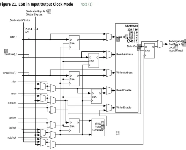
Input/Output Clock Mode
The input/output clock mode contains two clocks. One clock controls all registers for inputs into the ESB: data input,
WE,
RE, read address, and write address. The other clock controls the ESB data output registers. The ESB also supports clock enable and asynchronous clear signals; these signals also control the reading and writing of registers independently.
Input/output clock mode is commonly used for applications where the reads and writes occur at the same system frequency, but require different clock enable signals for the input and output registers. Figure 21 shows the ESB in input/output clock mode.
Figure 21. ESB in Input/Output Clock Mode Note (1)
Notes:
(1) All registers can be cleared asynchronously by ESB local interconnect signals, global signals, or the chip-wide reset.
(2) APEX 20KE devices have four dedicated clocks.
Dedicated Clocks
2 or 4 4
D ENA
Q
D ENA
Q
D ENA
Q
D ENA
Q
D ENA
Q data[ ]
rdaddress[ ]
wraddress[ ]
RAM/ROM 128 × 16 256 × 8 512 × 4 1,024 × 2 2,048 × 1 Data In
Read Address
Write Address
Read Enable
Write Enable Data Out
outclken
inclken
inclock
outclock
D ENA
Q
Write Pulse Generator rden
wren
Dedicated Inputs &
Global Signals
To MegaLAB, FastTrack &
Local Interconnect (2)
34 Altera Corporation
Single-Port Mode
The APEX 20K ESB also supports a single-port mode, which is used when simultaneous reads and writes are not required. See Figure 22.
Figure 22. ESB in Single-Port Mode Note (1)
Notes:
(1) All registers can be asynchronously cleared by ESB local interconnect signals, global signals, or the chip-wide reset.
(2) APEX 20KE devices have four dedicated clocks.
Content-Addressable Memory
In APEX 20KE devices, the ESB can implement CAM. CAM can be thought of as the inverse of RAM. When read, RAM outputs the data for a given address. Conversely, CAM outputs an address for a given data word. For example, if the data
FA12is stored in address
14, the CAM outputs
14when
FA12is driven into it.
CAM is used for high-speed search operations. When searching for data within a RAM block, the search is performed serially. Thus, finding a particular data word can take many cycles. CAM searches all addresses in parallel and outputs the address storing a particular word. When a match is found, a match flag is set high. Figure 23 shows the CAM block diagram.
Dedicated Clocks
2 or 4 4
D ENA
Q
D ENA
Q
D ENA
Q
D ENA
Q data[ ]
address[ ]
RAM/ROM 128 × 16 256 × 8 512 × 4 1,024 × 2 2,048 × 1 Data In
Read Address
Write Enable Data Out
outclken
inclken
inclock
outclock
Write Pulse Generator wren
Dedicated Inputs &
Global Signals
To MegaLAB, FastTrack &
Local Interconnect (2)
Figure 23. APEX 20KE CAM Block Diagram
CAM can be used in any application requiring high-speed searches, such as networking, communications, data compression, and cache
management.
The APEX 20KE on-chip CAM provides faster system performance than traditional discrete CAM. Integrating CAM and logic into the APEX 20KE device eliminates off-chip and on-chip delays, improving system performance.
When in CAM mode, the ESB implements 32-word, 32-bit CAM. Wider or deeper CAM can be implemented by combining multiple CAMs with some ancillary logic implemented in LEs. The Quartus software combines ESBs and LEs automatically to create larger CAMs.
CAM supports writing “don’t care” bits into words of the memory. The don’t-care bit can be used as a mask for CAM comparisons; any bit set to don’t-care has no effect on matches.
The output of the CAM can be encoded or unencoded. When encoded, the ESB outputs an encoded address of the data’s location. For instance, if the data is located in address
12, the ESB output is
12. When unencoded, the ESB uses its 16 outputs to show the location of the data over two clock cycles. In this case, if the data is located in address
12, the 12th output line goes high. When using unencoded outputs, two clock cycles are required to read the output, because a 16-bit output bus is used to show the status of 32 words.
The encoded output is better suited for designs that ensure duplicate data is not written into the CAM. If duplicate data is written into two locations, the CAM’s output will not be correct. If the CAM may contain duplicate data, the unencoded output is a better solution; CAM with unencoded outputs can distinguish multiple data locations.
CAM can be pre-loaded with data during configuration, or it can be written during system operation. In most cases, two clock cycles are required to write each word into CAM. When don’t-care bits are used, a third clock cycle is required.
wraddress[]
data[]
wren inclock inclocken inaclr
data_address[]
match outclock outclocken outaclr
36 Altera Corporation
f For more information on APEX 20KE devices and CAM, see Application
Note 119 (Implementing High-Speed Search Applications with APEX CAM).Driving Signals to the ESB
ESBs provide flexible options for driving control signals. Different clocks can be used for the ESB inputs and outputs. Registers can be inserted independently on the data input, data output, read address, write address,
WE, and
REsignals. The global signals and the local interconnect can drive the
WEand
REsignals. The global signals, dedicated clock pins, and local interconnect can drive the ESB clock signals. Because the LEs drive the local interconnect, the LEs can control the
WEand
REsignals and the ESB clock, clock enable, and asynchronous clear signals. Figure 24 shows the ESB control signal generation logic.
Figure 24. ESB Control Signal Generation
Note:
(1) APEX 20KE devices have four dedicated clocks.
An ESB is fed by the local interconnect, which is driven by adjacent LEs (for high-speed connection to the ESB) or the MegaLAB interconnect. The ESB can drive the local, MegaLAB, or FastTrack Interconnect routing structure to drive LEs and IOEs in the same MegaLAB structure or anywhere in the device.
RDEN WREN INCLOCK INCLKENA
OUTCLOCK OUTCLKENA Dedicated
Clocks Global Signals Local
Interconnect Local Interconnect Local Interconnect Local Interconnect
2 or 4 4
Local Interconnect Local
Interconnect INCLR OUTCLR
(1)
Implementing Logic in ROM
In addition to implementing logic with product terms, the ESB can implement logic functions when it is programmed with a read-only pattern during configuration, creating a large LUT. With LUTs,
combinatorial functions are implemented by looking up the results, rather than by computing them. This implementation of combinatorial functions can be faster than using algorithms implemented in general logic, a performance advantage that is further enhanced by the fast access times of ESBs. The large capacity of ESBs enables designers to implement complex functions in one logic level without the routing delays associated with linked LEs or distributed RAM blocks. Parameterized functions such as LPM functions can take advantage of the ESB automatically. Further, the Quartus software can implement portions of a design with ESBs where appropriate.
Programmable Speed/Power Control
APEX 20K ESBs offer a high-speed mode that supports very fast operation on an ESB-by-ESB basis. When high speed is not required, this feature can be turned off to reduce the ESB’s power dissipation by up to 50%. ESBs that run at low power incur a nominal timing delay adder. This Turbo Bit
TMoption is available for ESBs that implement product-term logic or memory functions. An ESB that is not used will be powered down so it does not consume DC current.
Designers can program each ESB in the APEX 20K device for either
high-speed or low-power operation. As a result, speed-critical paths in the
design can run at high speed, while the remaining paths operate at
reduced power.
38 Altera Corporation
I/O Structure The APEX 20K I/O element (IOE) contains a bidirectional I/O buffer and a register that can be used either as an input register for external data requiring fast setup times, or as an output register for data requiring fast clock-to-output performance. IOEs can be used as input, output, or bidirectional pins. For fast bidirectional I/O timing, LE registers using local routing can improve setup times and OE timing. The Quartus Compiler uses the programmable inversion option to invert signals from the row and column interconnect automatically where appropriate.
Because the APEX 20K IOE offers one output enable per pin, the Quartus Compiler can emulate open-drain operation efficiently.
The APEX 20K IOE includes programmable delays that can be activated to ensure zero hold times, minimum clock-to-output times, input IOE register-to-core register transfers, or core-to-output IOE register transfers.
A path in which a pin directly drives a register may require the delay to ensure zero hold time, whereas a path in which a pin drives a register through combinatorial logic may not require the delay.
Table 9 describes the APEX 20K programmable delays and their logic
options in the Quartus software.
The Quartus Compiler can program these delays automatically to minimize setup time while providing a zero hold time. Figure 25 shows how fast bidirectional I/Os are implemented in APEX 20K devices.
The register in the APEX 20K IOE can be programmed to power up high or low after configuration is complete. If it is programmed to power up low, an asynchronous clear can control the register. If it is programmed to power up high, the register cannot be asynchronously cleared or preset.
This feature is useful for cases where the APEX 20K device controls an active-low input or another device; it prevents inadvertent activation of the input upon power-up.
Table 9. APEX 20K Programmable Delay Chain
Programmable Delays Quartus Logic Option
Input Pin to Core Delay Decrease input delay to internal cells Input Pin to Input Register Delay Decrease input delay to input register Core to Output Register Delay Decrease input delay to output register Output Register tCO Delay Increase delay to output pinFigure 25. APEX 20K Bidirectional I/O Registers
VCC OE[7..0]
CLK[1..0]
ENA[5..0]
CLRn[1..0]
Peripheral Control Bus
CLRN
D Q