Title
C-12-41 LSI Implementation of a Bit-Parallel Cellular Multiplier
over GF(24) using Charge-Sharing Symmetric Adiabatic Logic.(
本文(Fulltext) )
Author(s)
MONTEIRO, Cancio; TAKAHASHI, Yasuhiro; SEKINE,
Toshikazu
Citation
[電子情報通信学会ソサイエティ大会講演論文集] vol.[2013]
no.[2] p.[101]-[101]
Issue Date
2013-09-03
Rights
copyright 2013 IEICE
Version
出版社版 (publisher version) postprint
URL
http://hdl.handle.net/20.500.12099/53352
Institute of Electronics, Information, and Communication Engineers
NII-Electronic Library Service
Institute ofElectionics, InEoimation, and CommunicationEngineeis2
O
1
3
ffS
i:fitureE\ft=vpFa=9xytt(rf(Jkft
C-12-41
LSI
Implementation
of
a
Bit-Parallel
Cellular
Multiplier
over
GF(24)
using
Charge-Sharing
Symmetric
Adiabatic
Logic.
Cancio
Monteiroi
Yhsuhiro
Takahashi2
[[bshikazu
Sekine2
Graduate
School
ofEngineering,
C;ifu
Universityifecu}ty
of Engineering,Gifu
IJniversity2Abstract
This
paperpresents
a verification ofthe
oporating speedin
abit-paraltel
cellu]ar multiplier overGF(24)
using a securedual-rail chargffsharing symmetric
adiabatic
logic.
The
multiplierLSI
uhip nieasuredin
thls
work waslabricated
usingO.IS
ptm
C]MOS
process
technology.
Maximum
power
clockfrequency
for
chip measurementis
5
MHz,
whereasthe
post-layout
simulationis
upto
50
MHz
aJidthe
pre-laorout
simulatioll reaches l25MHz
using
the
sameindividual
logic,
1
Introduction
Finitc
field
arithmetic
has
played
an
important
role
in
modern
coding
theory,
computer
algebra,
and
cryp-tographic
system.
Ftom
the
yiew
peint
of
the
crypto-graphic
hardware
implementation,
one ofthe
main is-suesis
relatedto
the security ofprocessed
iilformation.
Apart
form
the
securelogic
ability
to
wlthstand
side
channel
analysis
attacks,the
power
eMciency isalso adernand
of our society.Tb
the
best
of ourknowledge,
many works on securelogic
design
in
the
simulation
level
andfurther
in
the
LSI
implernentation
have
been
done
in
the
conventional CMOSlogic
operation,As
a result,thc
high
dynamic
power
consumptionbecomes
a challenge andthe
motivationin
our work.In
our approachfor
secureand
low-power
logic
implementa-tion,
we
have
designed
a
new securelogic
styletliat
is
based
on
the
a[liabatic switchingprinciple
[1].
The
full
customlayout
wasdesigned
in
cadence virtuosoIC6.1
withthe
chipsize
of 172×155
pam2
[2].
In
this
work,the
fabricated
LSI
chip measurementis
conducted.The
operating speed of the mukiplier inthe
LSI
ls
checked and compared withthe
prfflasout
andthe
post-layout
simulation result,2
LSI
Measurement
Result
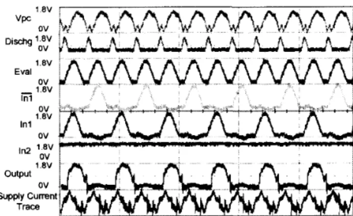
The
circuit schematic ofthe
bit-parallel
cellular
multiplier over
GF(24)
andthe
photomicrograph
areshown
in
Figs.
1(a),(b),
respectively,As
shownin
Fig.
(a)
that
the
inner
cell composes ofdual-ii'Lput
AND
andXOR
togic,
wherethose
individ-uallogic's
transistor
schematiccan
be
found
in
[1].
The
LSI
measurement result ofthe
input
andout-put
signals at1.25
MHz
power
clockfrequency
is
shownin
Fig,
2,
In
this
measurement,
the
in-put
signals
of
the
Inl=
{AO,Al,A2,A3,A4},
Jn2=
{BO,Bl,B2,B3,B4}="1",
thus
the
output
voltage
of a multiplier{CO,Cl,C2,C3,C4}
are correntlypre-duced
asOut="1".
The
Vpc
supply currentin
the
bottom
ofFlg,
2
indicates
that
the
peak
currentis
uniformly
plotted
which
may
resistiveto
side
channel
analysis attacks.
(a)
Cb)
Fig,
1
(a)
Circuit
structure of thebit-parallel
cellularmultiplier
over
GF(24),
(b)
Photomicrograph
of
the
bit-paJrallel
cellu]ar
multiplier overGF(24).
vpe ",:V
M.AAvgkkAV5A,bs'Ni'XA,A
Dischg'6tV;/
L:.k,"
A.iA.,.,A...LmaAw(・
'
/
t
Et:llD:vl' tu
s'
'
ov 1.ev lnl ov 1.ev 1ma ov 1,evOutpat ov I s,pp+y.C.'.rreniFig.
2
Input
and output signals ofthebit-parallel
cel-lular
multiplier oveTCF(24)
from
the measuremeiit re-sult.3
Conclusion
We
have
verified a multiplierlogic
functionality
in
the
LSI
measurement
that,
the
output
voltages
are
cor-rectly
measures,The
maximum operatingpower
clockfrequency
inthe
measurementis
5
MHz,
whichis
slowdown
from
50MHz
in thepost-layout
simulation and ahundred
times
speeddown
from
prelayout
simulationusing
the
sarne
individual
logic.
Referenoes
[11
C.
Monteiro,
Y.
Takahashi,
andT.
Sekine,
``Charge-sharingsymmetric
adiabatic
Logic
in
counterTneasure aguinst poweranalysis attacks at cell
leve1,"
thcrvetectronics
Jeurnat,
vol.44, no.6,
pp.496-503,
June
2013.
[2]
C.
Monteiro,
Y.
Talcahashi,
alldFl'.
Sekine,
"Lewpower
cure
CSSAL
bit-parallel
multiplier overGF(24)
in
O,18pm