リアルタイム追跡用アナログフェーズドアレイアン テナの開発
グアン, チャイ ユー
https://doi.org/10.15017/1931941
出版情報:Kyushu University, 2017, 博士(工学), 課程博士 バージョン:
権利関係:
Graduate School of Information Science and Electrical Engineering Kyushu University, Fukuoka, Japan.
Development of Analog Phased Array Antenna for Real-time Location System
by Guan Chai Eu
A thesis submitted to the Graduate School of Information Science and Electrical Engineering in partial fulfilment of the requirements for the degree of
Doctor of Engineering
Kyushu University, Fukuoka, Japan.
2018
GRADUATE SCHOOL OF INFORMATION SCIENCE AND ELECTRICAL ENGINEERING
KYUSHU UNIVERSITY Fukuoka, Japan
Thesis Title:
Development of Analog Phased Array Antenna for Real-time Location System
Prepared by: Guan Chai Eu
Supervisor : Professor Haruichi Kanaya, Dr. Eng.
Co-supervisor 1: Professor Kuniaki Yoshitomi, Dr. Eng.
Co-supervisor 2: Professor Kazutoshi Kato, Dr. Eng.
Date: March 2018
Kyushu University, Fukuoka, Japan.
To Whom It May Concern,
We hereby certify that this copy is a typical copy of the original Dr. Eng. (Doctor of Engineering) thesis of
Mr. Guan Chai Eu
Dissertation Title:
DEVELOPMENT OF ANALOG PHASED ARRAY ANTENNA FOR REAL-TIME LOCATION SYSTEM
Supervisor,
_______________________________
Prof. Haruichi Kanaya, Dr. Eng.
Department of Electronics,
Graduate School of Information Science and Electrical Engineering,
KYUSHU UNIVERSITY March, 2018.
i
Acknowledgements
First and foremost, I would like to express my deepest gratitude and sincere appreciation to my research supervisor, Professor Haruichi Kanaya for his guidance and support over the course of this research. I have benefited greatly from his perceptive and remarkable knowledge of my field of research. Inspirations gained from technical discussions with him have proven to be invaluable in defining my research direction. In addition, good research environment and hospitality offered by Professor Haruichi Kanaya becomes one of the most memorable experiences in my life.
Furthermore, I would like to thank to Professor Kuniaki Yoshitomi and Professor Kazutoshi Kato for serving on my dissertation committees. Their valuable suggestions are very useful in the improving quality of the dissertation. Their generosity in providing their expertise and advices has inspired me to engage in lifelong learning and being relevant to the organization and community that I will be attached to.
Interacting with my colleagues in RFIC and Microwave Communication Device laboratory has been rewarding, both personally and professionally. I am particularly indebted to every member in the laboratory whom unconditionally lent their kind support to me when I was a research student and after I become a PhD candidate. Many arduous evaluations and experiments became more rewarding with their assistance.
Besides, I would like to express my gratitude to our industry collaborators – Mr.Akira Ishikawa, Mr.Shugo Fukagawa and Mr.Ryuji Kitaya from Kyushu Ten. They assisted me in many aspects and their supports made this research became less strenuous.
Also, I would like to extend my gratitude to the university co-investigators: Mr. Tomoki Oda, Mr. Fumiya Iwai, Mr. Kota Tsugami and Mr. Takuhiro Ide, for their significant contributions in developing receiver module for the wireless locating system.
This dissertation would never have been completed without the sponsor and
support from Japan Ministry of Education, Culture, Sports, Science and Technology
(MEXT). I am extremely indebted to the Japan government for the financial aid given
and assigning me to learn from a supportive, dedicated, and profound research
supervisor. Thank you.
ii
Abstract
Global Positioning System (GPS) is widely used for locating and tracking objects due to their maturity and large scale implementation. Increase in the number of satellites and number of satellite systems spurs rapid development of detailed digital maps. Many vehicles used in government and commercial sectors, such as taxis, buses, ambulances, and fire trucks are equipped with navigation systems that not only show the current location but constantly trace the movement of vehicle from a monitoring center.
Business ventures such as Uber and Grab benefited from the advancement of GPS that leads to new mobile internet applications to complete the conventional public transport services. Uber and Grab-based applications enable prospective passengers to request door-to-door transport service via mobile phone booking.
From the point of view the security and traceability, demands for real-time location tracking of object or human in indoor environment increases. GPS (Global Positioning System), a satellite-based real-time location tracking system, is widely used in providing critical positioning capabilities to commercial users. Due to inability of transmitted signals to penetrate through the wall of building, GPS is unfitted for indoor environment, such as inside building and factory. Low accuracy in the range of 1 meter makes satellite-based location tracking system less suitable for indoor environments. On the other hand, the capability of time difference of arrival (TDOA) based radar, which operates at license-free high band UWB (Ultra-wide band, 7.25 GHz to 10 GHz), capable of estimating object location with the accuracy of 10 cm has been reported.
TDOA method estimates signal propagation distance by calculating difference between the time that signals were sent, and time that signals arrive at receiver. It was reported that transmitted pulse shorter than 1 ns is required for precise indoor object-tracing, so that time difference between incident and arrival signals can be exactly measured.
While UWB systems have a very good accuracy, their maximum operation range
is limited by few tens of meters. Realization of a system with high antenna gain for long
distance communication systems, such as object tracking in warehouse and factory,
becomes main challenge because maximum radiated power spectral density of the
existing system is limited by local laws and regulations.
iii The dissertation presents design methodology to increase antenna gain and scan angle in a wideband phased-array system in indoor environment. First part of this dissertation presents a 1x4 printed array antenna for multiple layers PCB. The goal of this work is to design an antenna with realized gain and input impedance less responsive to substrate thickness. Patch antenna fed by two-layer proximity coupled feed line is proposed to alleviate gain degradation caused by thin substrate. Fabricated antenna exhibits good radiation characteristics and a flat gain response from 7.7 to 8.3 GHz.
Besides, optimum separation between periodically spaced vias is analyzed and proposed to reduce propagation leakage in the dielectric region.
Second part of this dissertation presents the analysis and design of a full 360 degrees, harmonic-suppressed hybrid coupler phase shifter. Numerical and parametric analyses are used to find the equivalent circuit for circuit proposed. Simulation and measurement results demonstrated that fabricated phase shifter suppresses second harmonic and achieves phase shift range of 360 degrees. Next, harmonic-suppressed phase shifter with new reflective network is presented for phased-array system.
Continuous relative phase shift of 250 degrees and insertion loss variation less than 1 dB are achieved with 0-to-10V reverse bias voltages. It is observed that insertion loss variation is smaller than commercial phase shifters and phase shifters found in the literature.
Finally, last part of this dissertation presents the integration of antenna array,
power divider, phase shifter and parasitic antenna elements on multiple layers PCB to
realize phased array antenna. By placing parasitic antennas in between active antenna
arrays, it is found that mutual coupling effect between parasitic antennas and neighbor
active driven antenna increases scan angle range of phased array antenna. The measured
far-field radiation patterns of fabricated phased array antenna match to the simulation
results. Proposed work extends maximum scan range from 55 degrees to 60 degrees. In
this work, wide scan angle is realized by using phase shift range lower than phase shift
range required in conventional corporate-fed phased array antennas.
iv
Contents
Acknowledgements ……… .. … ....i
Abstract ……… ...ii
Contents ……… ... … .iv
List of Figures ……… ... … vi
List of Tables ……… .. … .. … ix
List of Abbreviations ……… . … x
CHAPTER 1: INTRODUCTION 1 1.1 Motivations ……… . 3
1.2 Research Objectives ……… ... 4
1.3 Thesis Outline ……… . 5
CHAPTER 2: PHASED ARRAY SYSTEM 7 2.1 Beam Steering Concept in Analog Phase Shifter ……… ... 9
2.2 Phase Shifting Techniques ……… . 12
2.3 Array Feeds 2.3.1 Series Array Feed ……… ... 14
2.3.2 Corporate Array Feed ……… . 15
2.4 Scan Angle Range of Analog Phased Array Antenna ……… 16
2.5 Antenna Gain and Radiation Efficiency ……… . 16
2.6 Chapter Summary ……… ... 19
References ……… .. 20
CHAPTER 3: LINEAR ARRAY ANTENNA 21 3.1 Antenna Design 3.1.1 Antenna Geometry ……… ... 22
3.1.2 Antenna Resonant Frequency ……… . ……… . 24
3.1.3 Fields Radiated in Patch in TM
xMode … .. ……… . 26
3.1.4 Antenna Input Impedance ……… 28
3.1.5 Antenna Array Principle ……… .. 29
3.2 Wilkinson Power Divider ……… . 31
3.3 Simulation and Measurement Results of Proposed Antenna Array ………… .. 35
v 3.4 Electromagnetic Leakage Suppression in Propagation Medium
3.4.1 Minimum Distance of Periodically Spaced Vias ……… .. 40
3.4.2 Design Verification and Implementation ……… .. 43
3.4.3 Simulation and Measurement Results ……… ... 45
3.5 Chapter Summary ……… ... 48
References.. ……… 49
CHAPTER 4: PHASE SHIFTER 4.1 Phase Shifter with Harmonic Suppression 4.1.1 Numerical Analysis ……… .. 54
4.1.2 Parametric Analysis ……… .. 61
4.1.3 Relationship of Series Inductance and Phase Shift Range ……… ... 62
4.1.4 Design Implementation and Fabrication ……… .. 66
4.1.5 Simulation and Measurement Results ……… .. 67
4.2 Phase Shifter with Discrete Reflective Loads 4.2.1 Circuit Analysis ……… 70
4.2.2 Design Implementation and Fabrication ……… .. 74
4.2.3 Simulation and Measurement Results ……… .. 75
4.3 Chapter Summary ……… .. 80
References ……… . 81
CHAPTER 5: PHASED ARRAY ANTENNA 83 5.1 Phased Array Antenna Architecture ……… ... 85
5.2 Parasitic Element For Scan Angle Enhancement ……… ... 87
5.3 Design Implementation and Fabrication ……… 90
5.4 Simulation and Measurement results 5.4.1 S-parameter ……… ... 91
5.4.2 Maximize Scan Angle Using Parasitic Antenna ……… .. 92
5.4.3 Far-field Radiation and Realized Gain ……… . 93
5.5 Chapter Summary ……… . 101
References ……… 103
CHAPTER 6: CONCLUSIONS AND FUTURE WORKS 105 6.1 Conclusions ……… 105
6.2 Future Works ……… . 108
References ……… .. 109
vi
List of Figures
Fig. 2.1 Digital beamforming architecture ……… .. 8
Fig. 2.2 Analog beamforming architecture ……… . 9
Fig. 2.3 Linear phased array antenna ……… .. 10
Fig. 2.4 Calculated radiation pattern of non-steering phased array antenna with (a) d = 0.5
λ0(b) d =
λ0……… .. 13
Fig. 2.5 Series and corporate array feeds ……… 15
Fig. 2.6 Calculated radiation pattern of 1x4 phased array antenna with
d=0.5λgand θ =180
˚, (a) Normalized radiation pattern. (b) Phase difference θ between antenna elements ……… . 17
Fig. 2.7 Phase between current I and voltage v, (a) Ideal case (b) lossy dielectric medium ……… ... 18
Fig. 3.1 Geometry of the proposed antenna ……… 22
Fig. 3.2 Electromagnetic field distribution in patch. ……… ... 23
Fig. 3.3 Structure of rectangular patch antenna ……… ... 24
Fig. 3.4 Excitation modes of rectangular patch antenna ……… . 26
Fig. 3.5 Perspective view of the patch and its radiation pattern. (a) Perspective view (b) xy-plane pattern (c) xz-plane pattern. ……… . 27
Fig. 3.6 Antenna input impedance in response to w
f2-to-w
f1ratio ……… .. 28
Fig. 3.7 Linear array consists of isotropic point sources equally-spaced with distance d ……… 30
Fig. 3.8 Array factor of two elements antenna verus spatial phase delay, ѱ… .. 31
Fig. 3.9 Three ports power divider. (a) Power divider with dividing ratio , r (b) Wilkinson power divider ……… ... 32
Fig. 3.10 Transmission line circuit model of Wilkinson power divider ………… 32
Fig. 3.11 Power source with source impedance matched to the transmission line ……… 34
Fig. 3.12 Gain drop in conventional patch antenna and proposed antenna at xz- plane, in response to substrate thickness reduction ……… .. 36
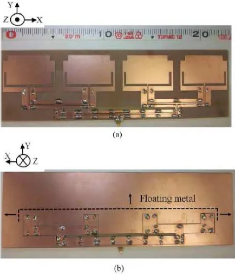
Fig. 3.13 Photograph of the fabricated array antenna ……… . 36
Fig. 3.14 Antenna input impedance measurement with Keysight 8722C Network analyzer ……… .. 37
Fig. 3.15 Radiation pattern measurement setup in anechoic chamber ………… .. 37
Fig. 3.16
S11and maximum realized gains of the proposed array antenna. Simulations (solid) and measurements (dashed) ……… .. 38
Fig. 3.17 Simulated (solid) and measured (dashed) radiation patterns of the proposed array antenna at 8 GHz: (a) xz plane, (b) yz plane ……… .. 39
Fig. 3.18 Geometry of the CBCPW with periodically spaced vias ………… .. 41
Fig. 3.19 Region of interest for the CBCPW with periodically spaced vias … . 42
Fig. 3.20 Layouts of antenna array fed by different topology. (a) CPW with air
bridges. (b) CBCPW with a periodic spaced-via ……… ... 44
vii Fig. 3.21 Fabricated 4x1 antenna array with the CBCPW feed network
(size=234 mm x 71 mm). (a) Top view. (b) Bottom
view ……… ... 45 Fig. 3.22 Measured reflection coefficient and achieved gain of the CPW-fed
and the CBCPW-fed antenna arrays ……… . 46 Fig. 3.23 Radiation pattern of 4x1 CBCPW-fed antenna array.
(a) xz-plane. (b) yz-plane ……… ... ………… . 47 Fig. 4.1 Digital phase shifter, (a) Circuit block diagram (b) I-Q relationship … 52 Fig. 4.2 Null in phased array antenna due to destructive interference between
phase shifter and antenna elements ……… 54 Fig. 4.3 Schematic diagram of π -section low pass filter (LPF) ……… ... 55 Fig. 4.4 Schematic of the conventional RTPS ……… . 57 Fig. 4.5 Schematic of proposed phase shifter with harmonic suppression …… .. 57 Fig. 4.6 Calculated relative phase shift versus port impedance ratio r
z(Z
qw= 20 Ω,
Ls=0.45nH, C
min=0.45pF, C
max=3.1pF and R
s=2.5Ω…… . 59 Fig. 4.7 Transmission line of the hybrid coupler. (a) Quarter wavelength
transmission line. (b) Distributed elements π -section filter ………… .. 59 Fig. 4.8 Parametric variation of the electrical length
θlof the transmission line
to obtain r
z=2 (a) Z
i2versus
θlvariation. (b) Z
o2versus
θlvariation … . 63 Fig. 4.9 Theoretical calculation of the relative phase shift versus varactor bias
voltage (Ls varies) ……… .. 65
Fig. 4.10 Theoretical calculation of the relative phase shift versus varactor bias
voltage (Z
qwvaries) ……… 65
Fig. 4.11 Layout of the full- 360 ˚, harmonic -suppressed hybrid coupler phase
shifter ……… .. 66
Fig. 4.12 A full 360◦, harmonic-suppressed hybrid coupler phase shifter (left)
and π -section LPF (right) ……… ... 67 Fig. 4.13 Second harmonic suppression of the π -section LPF at 17.2 GHz. (a)
Simulation (dashed) using HFSS (b) Measurement (solid) ………… . 68 Fig. 4.14 Second harmonic suppression of the proposed phase shifter, in
comparison with conventional phase shifter. S represents simulation
results from HFSS, and M represents measurements ……… 68 Fig. 4.15 Relative phase shift versus varactor bias voltage evaluated at
fundamental frequency of 8.6GHz. Simulation (solid) result from
HFSS, and measurement (dashed) ……… . 69 Fig. 4.16 |S11| (black), |S22|(blue), and |S21|(grey) of the phase shifter at
various varactor bias voltage Vb. (a) Simulations (b) Measurements... 69 Fig. 4.17 Schematic diagram of phase shifter with discrete reflective loads … .. 70 Fig. 4.18 Calculated relative phase shift versus tuning range of varactor at 8.6
GHz (L
s=0.2nH, Z
03=25Ω , and R
s=2 Ω ) ……… 72 Fig. 4.19 Calculated insertion loss of phase shifter versus tuning range of
varactor
(Le
=0.4 nH, L
s=0.2nH, C
min=0.2pF, C
max=1pF, Z
03=25Ω , and R
s=2 Ω ) 73 Fig. 4.20 Calculated phase shift across frequencies of interest
(Le
=0.4 nH, L
s=0.2nH, Z
03=25Ω , and R
s=2 Ω ) ……… 73
viii
Fig. 4.21 Layout of phase shifter with discrete loads ……… 74
Fig. 4.22 Input return loss S
11of phase shifter, simulation (solid) and measurement (dashed) ……… .. 75
Fig. 4.23 Output return loss S
22of phase shifter, simulation (solid) and measurement (dashed) ……… 76
Fig. 4.24 Insertion loss S
21of phase shifter, simulation (solid) and measurement (dashed). ……… ... 76
Fig. 4.25 Insertion phase
ϕS
21of phase shifter output, simulation (solid) and measurement (dashed) ……… .. …… 77
Fig. 4.26 Electric field distribution of phase shifter with reflection loads separated by quarter wave-length transmission line ……… .. 78
Fig. 4.27 Electric field of proposed phase shifter with discrete reflection loads.. 78
Fig. 5.1 Corporate-fed phased array antenna with the proposed phase shifter... 86
Fig. 5.2 Phase shifter with different reflection loads topology. (a) Conventional phase shifter. (b) Proposed phase shifter with discrete reflective loads ……… . 86
Fig. 5.3 Mutual coupling between active dipole antenna and parasitic antenna 89 Fig. 5.4 Electric field distribution at scanning angle of +30
˚………..……….89
Fig. 5.5 Prototype of phased array antenna (74.5 mm x 46.8 mm). (a) Top view. (b) Bottom view ……… .. 90
Fig. 5.6 Phased antenna measurement in anechoic chamber ……… . …… . 91
Fig. 5.7 Return loss of the phased array antenna at various scan angle …… .. … 92
Fig. 5.8 Induced current at the floating parasitic antenna ……… ... 92
Fig. 5.9 Radiation pattern at scan angle, θ =0
˚ and center frequency, fc=8.6 GHz (xz-plane). (a) Simulation. (b) Measurement.(c) Simulated 3D radiation pattern ……… . 93
Fig. 5.10 Radiation pattern at scan angle, θ =
−10
˚ and center frequency, fc=8.6 GHz (xz-plane). (a) Simulation, (b) Measurement. (c) Simulated 3Dradiation pattern ……… .... 94
Fig. 5.11 Radiation pattern at scan angle, θ =+10
˚ and center frequency, fc=8.6 GHz (xz-plane). (a) Simulation. (b) Measurement. (c) Simulated 3Dpattern ……… 94
Fig. 5.12 Radiation pattern at scan angle, θ =
−30
˚ and center frequency, fc=8.6 GHz (xz-plane). (a) Simulation. (b) Simulated 3D pattern……… . … .. 95
Fig. 5.13 Radiation pattern at scan angle, θ =+30
˚ and center frequency, fc=8.6 GHz (xz-plane). (a) Simulation. (b) Simulated 3D pattern… . ……… ... 95
Fig. 5.14 Simulated realized gain of phased array antenna at xy-plane (max. scan angle θ =
±30
˚) ……… .. 96
Fig. 5.15 Broadside radiation beam at multiple frequencies (no beam steering).. 97
Fig. 5.16 Scan angle of
−15
˚at multiple frequencies ……… .. ………… . 97
Fig. 5.17 Scan angle of +15
˚at multiple frequencies ……… 98
Fig. 5.18 Scan angle of
−30
˚at multiple frequencies ……… .. ……… . 98
Fig. 5.19 Scan angle of +30
˚at multiple frequencies ……… 99
Fig. 5.20 Schematic of DC-to-DC step up converter (LMR62421) and its
subsidiary components ……… ... 102
ix
List of Tables
Table 3.1 Design parameters of the proposed antenna ……… .. 28 Table 3.2 Resultant voltages from superposition analysis ……… 34 Table 3.3 Wilkinson power divider S parameters at input and output ports … . 35 Table 4.1 Design parameters of the RTPS (r
z=2) ……… 65 Table 4.2 Parameters of π -section LPF obtained from numeric and parametric
analysis ……… . 66
Table 4.3 Parameters of π -section LPF (unit in mm) ……… .. 66 Table 4.4 Dimension of phase shifter with discrete loads. (unit in mm) ……… . 74 Table 4.5 Comparison of proposed works against other phase shifters found in
the literature ……… .. 79
Table 5.1 Progressive phase shift required for beam steering from
−25
˚to
+25
˚……….…85 Table 5.2
Comparison of phased array antenna with and without parasiticelement……….
87 Table 5.3 Realized gain at difference scan angle at the center frequency, f
c=8.6
GHz ……… .. 99 Table 5.4
Comparison of the proposed phased array antenna against othersteerable antennas found in the literature………
100
x
List of Abbreviations
ADC - Analog to digital converter
AF - Antenna factor
CBCPW - conductor backed co-planar waveguide
CMOS -Complementary metal-oxide semiconductor CPW - co-planar waveguide
DBF - Digital beamforming
DC - Direct current
DOA - Direction of arrival DSP - Digital signal processor DUT - Device under test
ESPAR - Electronically steerable passive array radiator FPGA - Field programmable gate array
IF - Intermediate frequency
ISM - Industrial, science and medical LMS - Least mean square
LNA - Low noise amplifier
LO - Local oscillator
LTCC - Low temperature co-fired ceramic
MIMO - Multiple Input Multiple Output
MMIC - Monolithic microwave integrated circuit MSL - Microstrip line
PCB - Patterned circuit board
RF - Radio frequency
RLS - Reclusive least square
RTPS - Reflective-type phase shifter
SINR - Signal to noise interference
UWB - Ultra-wide band
1
Chapter 1
Introduction
As wireless technology progresses, antennas are evolved in order to keep its pace to the latest demands of the market. Reconfigurable antenna in wireless communication system offers spatial directivity and antenna gain to increase spectral efficiency.
Directivity of antenna array in wireless communication with beam steering capability can be adapted to a particular transmit or receive angle. Generally, antenna elements with the same radiation patterns and polarizations are used to populate phased array system, which leads to performance enhancement in terms of peak gain and beam width characteristics.
In satellite communication, antenna on the surface of earth is fixed and pointed to satellites located in geosynchronous orbit. Constant communication is maintained because orbital periods of satellites are same as the Earth's rotation period. Reflector antenna, which has high gain, is preferred in point-to-point communication. Antenna array with beam steering capability is preferred when simultaneous communication between stationary earth station and several geostationary (GEO) satellites is required.
In cellular communications and Wi-Fi system, antenna array with beam steering
capability is deployed in multiple input multiple output (MIMO) system. MIMO systems
benefit from increase in data rate and network capacity.
2 Multiple, spatially separate data can be transmitted over the same frequency band via beam steering technique. Besides, beam steerable antenna can dynamically respond to the propagation environment to minimize multipath fading.
In RFID systems, beam steering technology is the backbone of wireless locating and tracing system. Its implementation allows real-time tracking of goods and products, for more efficient storage and sequence planning. Radiation beam can be adaptively steered from one spot to another spot in the surveillance region without any additional readers. Several commercial UWB radars, which use low energy spectral density based on chirp-spread spectrum signals, are able to provide minimum accuracy of few centimeters such as, PulsON 440 module, Decawave Scensor DW1000 and Ubisense Dimension4.
In automotive industry, Lidar (Light radar), which is based on beam steering technology, are widely researched for the next-generation car sensor. It detects objects with optical pulses and produces a set of data points to estimate the distance of nearby objects. On 2016 consumer electronics show (CES) exhibition, Quanergy Systems, which is based in Sunnyvale (California), demonstrated a prototype solid-state Lidar sensor designed for driverless car. Representative from Quanergy quoted that its sensor will cost 250 USD in volume production. Currently, industry players are working hard towards their final goal of realizing solid-state Lidar sensor, which is capable of detecting 100 m object with a selling price of 10 USD per chip.
Beam steering technology can be realized on patterned circuit board (PCB), low
temperature co-fired ceramic (LTCC)or silicon-based technologies such as complementary metal-oxide semiconductor (CMOS) and silicon germanium (SiGe). For millimeter-wave band wireless communication system, compound semiconductors, e.g.
indium phosphide (InP) and gallium arsenide (GaAs), are preferred, irrespective of their
high fabrication cost and complex fabrication process. Currently, the cost of CMOS or
monolithic microwave integrated circuit (MMIC) chip fabrication and complexity of
phased array antennas are the main impediments to their deployment in any large scale
commercial application.
3 X-band spectrum, as well as high band ultra-wideband (UWB) spectrum, has short wavelength (<5 cm). They are good candidates for wireless locating system that requires accuracy resolution of 10 cm for object tracking. Development of phased array system operates at X-band on patterned circuit board (PCB) will reduce production cost and extend the deployment of phased array antenna to a wide range of consumer applications. Usually, microwave devices operate X-band or high band UWB spectrums are fabricated on CMOS or compound semiconductors. Implementation of the microwave devices on standard PCB that has higher tangent loss than CMOS and compound semiconductors, poses several challenges in terms of substrate loss, module size, dispersion characteristics in the microstrip transmission line and etc.
This
dissertation investigates on the high band UWB phased array antennaimplemented on patterned circuit board (PCB) to achieve good cost versus performance.
First, designs of phased array antennas found in the literature are taken as reference models. Modular approach is adopted to develop microwave devices, i.e. antenna, phase shifter, and power distribution network, separately. Next, all microwave devices are integrated into a single module on multiple layers PCB. Viable solutions are then proposed to realize phased array antenna that meet requirements of commercial applications such as realized gain, scan angle, power consumption, operation bandwidth, control voltages, and manufacturing cost.
1.1 Motivations
Wireless communication systems in the consumer market normally operate at 2.4 and 5 GHz frequency ranges. However, the growing demands for higher data rates spur the development of wireless communication system at higher frequencies because significantly wide bandwidth can be obtained as operating frequency is increased.
Wavelength at higher frequencies, e.g. X-band and above, is shorter than the ones in 2.4 GHz and 5 GHz. As opposed to wavelength at 2.4 GHz or 5 GHz, X-band signal has a shorter wavelength, in which signal could not penetrate through walls and ceilings.
Short wavelength has good isolation in indoor environment enables frequency reuse in
order to extend the number of users.
4 In indoor environments such as the factory and airport checked luggage area, wide operation bandwidth and frequency reuse are required for real-time object tracking system. From the point of view the security and traceability, the growth of real-time location estimation of object or human in indoor environment is expected. In outdoor environment, a satellite-based real-time location tracking system, GPS (Global Positioning System) is widely used in providing critical positioning capabilities to users.
Due to its inability of transmitted signals to penetrate through the wall of building, airborne GPS is unfitted for indoor environment, such as inside building and factory.
On the other hand, the capability of time difference of arrival (TDOA)-based radar to estimate object location with the accuracy of 10 cm has been reported. It operates in license-free high band UWB (ultra-wide band, 7.25 GHz to 10 GHz). TDOA method estimates signal propagation distance by calculating difference between the exact times that signals were sent, and time that signals arrive at receiver. Maximum radiated power spectral density of the present system is limited by local laws and regulations. By increasing antenna gain in a system, communication distance can be extended in system with restricted power spectral density.
This dissertation presents a design methodology to increase antenna gain and maximize scan angle in phased array systems with a limited bias voltage. PCB manufacturing process is preferred because of its low fabrication cost and ease of implementation. Best to author
’s knowledge, implementation of module-based phased array system at X-band using PCB manufacturing process has not been reported prior to this work. Considering the merit of cost versus performance of PCB-based phased array antenna, the development of beam steering system for real time location system is investigated thoroughly in this dissertation.
1.2 Research Objectives
The objectives of this thesis are to develop phased array antenna in a single module, which has the following unique features that can be summarize as:
(1) Intermodulation Distortion Reduction: Designed phase shifter must be capable of
suppressing high order harmonics on transmitter and receiver paths.
5 Suppression of high order harmonics at the RF front-end reduces intermodulation distortion at low noise amplifier (LNA) in the receiver path.
(2) Beam Squint: Beam squint refers to the changes in scanning angle of phased array antenna when the operating frequency is changed. Beam squint is commonly found in series-fed phased array antenna because of large group delay from accumulated phase shift. Corporate-fed phased array antenna has minimum beam squint but strict requirement for large phase shift range in individual phase shifter limits scan angle of the adaptive antenna array.
(3) Scan Angle with Low Bias Voltage: To achieve large scan angle range, large progressive phase shift range is required in phased array antenna. My research objective is to widen scan angle of phased array antenna with restricted phase shift range, by using 10 V bias voltage. Parasitic antenna elements are introduced to extend original scan angle, in order to overcome phase shift limitation imposed by phase shifters.
1.3 Thesis Outline
The dissertation is organized in 6 chapters to define and explain on the development of analog phased array antenna. Concept of beam steering in analog phased array antenna is provided in Chapter 2. Phased array system architecture and possible phase shifting techniques are then discussed. Issue related to grating lobes in the radiation pattern caused by separation distance between adjacent antenna elements is highlighted. Next, power distribution network of the antenna elements is explored to ensure uniform power distribution and evade some issues related to scan angle across frequencies of interest. The relationship of scan angle with progressive phase shift and separation distance between adjacent antennas is defined.
Chapter 3 discusses the implementation of linear antenna array on multiple layers
PCB process. Antenna elements are fabricated on 1.6 mm while power distribution
network is fabricated on 0.2 mm PCB. Antenna elements and its distribution network are
combined into single module using multiple layers PCB to achieve compact and low
profile structure.
6 Two layer proximity coupling is introduced in slotted patch antenna for impedance matching purpose. In addition, periodically spaced vias structure is proposed for radiation suppression in the transmission line. At the end of the section, simulation and measurement results are presented to validate design concept introduced.
Chapter 4 presents the analysis and design of a full 360 degrees, harmonic- suppressed hybrid coupler phase shifter. Numerical and parametric analyses are introduced as tools of analysis. Simulation and measurement results demonstrate that fabricated phase shifter suppresses higher harmonics and achieves relative phase shift range of 360
˚. Next, harmonic-suppressed phase shifter with reflective network constructed from discrete varactors and inductors is proposed. Continuous relative phase shift of 250
˚and insertion loss variation with less than 1 dB are achieved with 10 V reverse bias voltage. The loss variation obtained is less than commercial phase shifters and phase shifters found in the literature.
Chapter 5 presents the integration of antenna array, power divider, phase shifter and parasitic antenna elements fabricated on multiple layers PCB to form phased array antenna. By placing parasitic antennas in between active antenna arrays, it is found that mutual coupling between active antennas and parasitic antennas increases scan angle range of phased array antenna. The measured far-field radiation patterns of the fabricated phased array antenna match to simulation results. Proposed parasitic antennas extend the maximum scan angle range from 50
˚to 60
˚. Proposed design technique enables wide scan angle to be achieved by phase shifter with limited phase shift range.
Required relative phase shift range for
±30
˚scan angle is less than other commercially available phased array system and phased array antennas found in the literature.
In the last chapter, contributions from all works and techniques are summarized.
Realization of phased array antenna with beam steering capability at device level and
system level are concluded. Besides, other prospective technique to improve the gain of
phased array system across wideband is reviewed.
7
Chapter 2
Phased Array Systems
The presence of phased array antenna enables antenna beam to be steered by electronic mean. Beam is steered by controlling phase and amplitude of incoming RF signals of phased array antenna. Beam steering techniques can be classified into analog and digital beamforming. Digital beamforming (DBF) architecture offers several sophisticate features, including multiple beams forming capability, direction of arrival (DOA) estimation, and good signal-to-interference noise ratio (SINR). Fig 2.1 shows the block diagram of a DBF antenna. DBF architecture consists of orthogonal transform unit and field programmable gate array (FPGA) to deliver amplitude and phase weights to antenna elements. Orthogonal transformation unit separates incoming intermediate frequency (IF) signals into in-phase
I, and quadrature Q components. The modulatedcomplex signals of antenna beams are processed by FPGA. Adaptive algorithm such as Least Mean Square (LMS), Recursive Least Square (RLS) and Conjugate Gradient Method (CGM) is utilized to compute the array weights [1]-[3]. The computed weights are downconverted to intermediate frequency (IF) signals and distributed to antenna elements for beam steering.
The analog approach, on the other hand, is less capable to execute the
same functionalities that DBF does. Fig 2.2 depicts two architectures of phased array
antenna using analog approach. As we can see, analog beamforming architectures
require neither analog-to-digital converters (ADCs) nor FPGA for complex amplitude
and phase distributions.
8
Analog approach offers low DC power consumption and affordable fabrication cost because of the absence of high-priced FPGA and ADCs. Architecture in Fig. 2.2(a) shows analog beamforming architecture, where complex weight is applied to the signal at radio frequency (RF) stage. The architecture is not suitable for system designated at frequency above Ku-band because off-the-shelf phase shifter operates at Ku-band is scarce; even if it were available, it should be expensive due to the low demand-to-supply ratio. RF complementary metal oxide semiconductor (RF-CMOS) and patterned circuit board (PCB) technology are the most common technologies used to fabricate phase shifter. For RF-CMOS phase shifter, transient frequency
ftof the gate transistor limits operation frequency of the device. PCB-based phase shifter can be deployed at high frequency; nevertheless, severe dielectric loss at high frequency due to tangent loss of dielectric material is inevitable. For system suffered from high attenuation at high frequency, variable gain amplifier was introduced to amplify weak RF signal [4].
Another technique to overcome severe attenuation at high frequency is demonstrated in Fig. 2.2(b), where phase shifting is implemented at intermediate frequency (IF) stage. In this architecture, RF signals are down-converted to IF signal for its phase to be shifted using phase shifters operate at IF-stage.
Fig. 2.1 Digital beamforming architecture.
ADC ADC ADC ADC
w w
w w
LO
FPGA
Orthogonal Transform Beamformer
Antenna
9
Fig. 2.2 Analog beamforming architecture. (a) RF Phase Shifting. (b) IF Phase Shifting.
2.1 Beam Steering Concept in Analog Phase Array Antenna
The history of analog beamforming technique dates back to the Butler matrix beamforming network consists of hybrid coupler and fixed phase shifters, that steers beam in discrete manner [5]. Researches on analog beam steering proliferated when analog phase shifters with continuous phase shift were proposed to replace butler matrix.
Block diagram of an
n-element phased array system is shown in Fig. 2.3. n-elementantennas are equally spaced by a distance,
d, along a linear axis. For simplicity, wediscuss only the receiver case, where similar concepts are held for transmitter due to the reciprocity concepts. Separate variable time delays are incorporated at each signal path to control the phase of the signals before all the signals are combined at the power combiner. Fig. 2.3 shows plane-wave beam incidents upon the antenna array at an angle
of θ to the normal direction.Due to the spacing between the adjacent antennas, the beam reached successive antennas at different time constant.
RF Power combiner
LO
IF
(a) (b)
IF Power combiner LO
IF
10
Fig. 2.3 Linear phased array antenna.
To derive array factor in linear phased array antenna, we do not consider mutual coupling between adjacent antenna elements for the sake of simplicity. Assume that all the elements in array are isotropic, and they are driven at the same phase and power, the resultant beam will radiate at broadside direction; perpendicular to the plane where they are mounted to. For broadside direction, radiation will spread along
z direction in Fig.2.3. When beam is steered, resultant field of radiated beam is a function of phase difference between adjacent antenna elements when the distance between the array elements,
d, is fixed and spaced apart by one-half free space wavelength ( 0/2). If we apply a progressive phase shift to the inter-stage array elements, the beam can be directed towards desired scan angle, for example,
θ, as shown in Fig. 2.3. In general, radiation pattern of uniformly-spaced array antenna can be represented by [6]
𝑆 𝜃 = ∑ 𝑆 𝜃 𝑆𝐴𝐹 𝜃 = 𝑆 𝜃 ∑ 𝑁− sin𝜃+𝛼 , .
𝑁
= 𝑁
=
where
𝛼represents phase taper on each path of antenna element.
Antenna
Phase Shifter
z-axis
Far-field radiation
11 Sel
(
θ) represents element factor of antenna elements, k
0is the free space wavenumber,
αis phase difference between adjacent antenna, and n
is number of antenna elements.
Array factor of linear array radiation pattern is written as
𝑆𝐴𝐹 𝜃 = ∑ 𝑁− 𝛹, .
𝑁
=
where
𝛹 = sin 𝜃 + 𝛼. .In eq. (2.3), we may recognise a finite geometric series. If both sides of this equation are multiplied with
𝛹, we get
𝑆𝐴𝐹 𝜃 𝛹 = 𝑁𝛹+ 𝑁− 𝛹 + ⋯ + 𝛹 + 𝛹 . .
Next, eq. (2.3) is subtracted from eq. (2.5), then we obtain
𝑆𝐴𝐹 𝜃 ( 𝛹− ) = ( 𝑁𝛹− ) .
which may be written, after splitting and rearranging the exponential terms, as
𝑆𝐴𝐹 𝜃 =
𝑁𝛹 𝑗𝑁𝛹− −𝑗𝑁𝛹
𝛹( 𝛹− − 𝛹)= 𝑁− 𝛹sin 𝑁𝛹
sin 𝛹 , .
Neglecting phase factor,
𝑁− 𝛹,
|𝑆𝐴𝐹 𝜃 | = |sin 𝑁𝛹
sin 𝛹 | . .
|𝑆𝐴𝐹 𝜃 | = |sin 𝑁 sin 𝜃 + 𝛼
sin sin 𝜃 + 𝛼 | . .
To steer beam to desired direction, progressive phase taper,
an, must be applied touniformly-spaced antenna elements. Separation distance between antenna elements, d, is
12
crucial to avoid unwanted radiation beam, known as grating lobes. Grating lobe appears when the array factor repeats itself, as reported in [3].
Grating lobes, which have same radiation strength as main beam, will appear along with the main beam if d is set too large. It occurs whenever the argument
𝛹in eq.
(2.4) is an integer multiple of
𝜋and it can be written as
𝛹 = 𝜋. = , , … , .
First grating lobe occurs when
𝜆 sin𝜃 − sin𝜃 = , = , , … , (2.12)
By rearranging eq. (2.12), grating lobe in uniformly-spaced phased array antenna can be
avoided if separating distance between antenna elements satisfies
< sin𝜃 − sin𝜃 . .
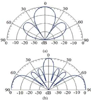
Fig. 2.4 shows radiation pattern of one dimension linear array antenna with and without the presence of grating lobes. Antenna elements are cosines waveform. Directivity of antenna array composed of cascading 4 identical, equidistant antenna elements is plotted.
Grating lobes occur when separation distance between antenna elements
d is increasedfrom one-half guided wavelength (0.5
λ0) to one wavelength (
λ0).
2.2 Phase Shifting Techniques
Phase shifter is a core device in analog phased array radar systems, as briefed in the previous section. We will take a look on parameters in RF signal which can be manipulated to accomplish a relative phase shift in this section. Phase of signals can be derived by assuming the signals to be time harmonic, as follows:
𝜔 = cos 𝜔 ,
(2.14)
where
𝜔 = 𝜋 ,is the frequency of travelling wave.
13
(a)
(b)
Fig. 2.4 Calculated radiation pattern of non-steering phased array antenna with (a) d =0.5
λ0and (b) d =
λ0 .Time, t, is expressed as the distance, l, travelled by signal over propagation velocity of the signal c, so that we find for phase of travelling wave as,
𝜔 = 𝜋 √𝜀
, (2.15) where
εis the permittivity, and is the permeability of the propagation medium.
Variables (
, , 𝜀,) listed in eq. (2.15) implicitly shows all parameters required to adjust phase of a signal. Relative phase shift are achieved, as follows:
adjusting phase by changing electrical length of transmission line (l);
adjusting phase by varying frequency of RF signal (f);
adjusting phase by changing permittivity of medium for signal propagation (
ε);
adjusting phase by changing permeability of medium for signal propagation ( ).
14 2.3 Array Feeds
Feeding network is the backbone in antenna arrays, in which it combines a number of antenna elements, to achieve high gain. Required phase shift range for phased array antenna to steer beam to the maximum scan angle depends on the type of feeding network used. Generally, antenna array can be categorized based on the way antenna elements are fed in an array network. When the array elements are in series along array feed,
the array is termed “series”.On the other hand
, the array is termed “shunt”when the elements are in parallel with array feed. Shunt feed is also known as corporate feed.
Series and corporate feeds are the most common feeding network available for phased array antenna.
2.3.1 Series Array Feed
Fig. 2.5 presents series-fed network consists of
N antenna elements and (N−1) phase shifters connected in series. To obtain broadside radiation, antenna elements are fed in-phase and series array feed is adjusted to a particular factor of wavelength of the operating signal. Input and output impedances of each antenna must be customized individually in order to match to the
transmission line’s characteristic impedance. The cumulative nature of the phase shift in series array feed enables the realization of a wide steering angle with a small phase shift range. As the signal travels away from the source in series array feed, antenna elements and phase shifters connected in series withdraw power from transmission line. For antenna elements located far away from the RF source, power delivered to the antenna elements is reduced.
When the number of elements in array antenna expands, this may lead to uneven
power distribution to antenna elements that must be accounted for array factor
calculation. Furthermore, accumulated phase shift in series-fed network leads to beam
squint and limits operating bandwidth of phased array antenna.
15
Fig. 2.5 Series and corporate array feeds.
2.3.2 Corporate Array Feed
Antenna elements arranged in parallel to the array feed is known as corporate-fed network. N antenna elements and N phase shifters are connected in parallel to form corporate feed. Owning to the fact that phase shifter is connected individually to antenna element, large phase shift range is required to realize wide beam steering angle. The required amount of phase shift is higher than series array feed by a factor of
N−1, in which N is the number of antenna elements in the phased array system. RF power is distributed evenly to each antenna element via equally split, 2-way power dividers cascaded in nested structure as illustrated in Fig. 2.5. In corporate-fed network, distance travelled by RF signals from the source to the array elements is same in terms of electrical length.
Antenna elements in corporate-fed network are equidistant from source. This allows radiated power to be distributed uniformly to generate maximum directivity at desired angle for a given aperture size. Side lobes level in corporate-fed antenna array can be suppressed by increasing number of antenna elements or distributing non-uniform amplitude with determined optimal weights for each antenna elements.
ϕ ϕ ϕ Feed 0 ϕ 2ϕ 3ϕ
Feed
Series array feed Parallel array feed
Required phase shift range for phase shifter Ѱ = 0~+3ϕ
Required phase shift range for phase shifter Ѱ = 0 ~+ϕ
16 2.4 Scan Angle Range of Analog Phased Array Antenna
Scan range is referred to the maximum scan angle of beam that can be steered away from broadside without the appearance of grating lobes in the principal planes. As we have seen in Fig. 2.4, grating lobes occur in the principal plane upon enlarging separation distance between antenna elements to
λ0. In other words, grating lobe occurs when separation distance
dis more than one free space wavelength (d
≥ λ0) for the broadside linear array antenna, in a non-scanning situation.
To steering beam in any angle without a grating lobe being present in the principal place, new equation is deduced from eq.(2.13) as follows,
< | + 𝑖 𝜃 𝑎𝑥| . .
Maximum scan angle without any grating lobes depends on the separation distance d. Eq.
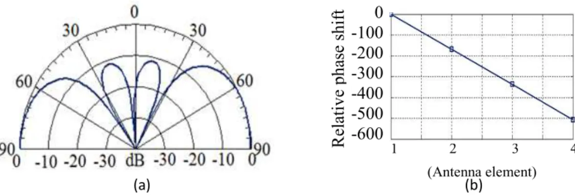
(2.13) implicitly indicates that grating lobes will appear even if separation distance between inter-stage antenna elements is kept less than one free-space wavelength, given than beam is over-steered. Fig. 2.6 shows calculated radiation pattern of 1x 4 phased array antenna with separation distance between antenna element,
d=0.5 g, and progressive phase difference,
θ=16
0˚.Progressive phase difference,
θ, is chosen to violate eq. (2.16) to demonstrate the occurrence of grating lobes.
Progressive phase shift required for grating lobe-free beam steering, can be written as
ϕ = ˚・ sin
. .
2.5 Antenna Gain and Radiation Efficiency
For direct current (DC) or alternate current (AC) transmission line, energy loss
can be ignored when power is transferred from one point to another point, separated by
distance,
d. Power transfer efficiency in a device or transmission line is defined as theratio of the output power divided by the input power. Resistance of material inhibits in
the carrier is the primarily factor of power loss in DC transmission line.
17
If we take a look on high frequency signal propagation in device such as antenna, there are several factors that lead to mismatch between radiated power in the free space and power delivered to the antenna.
Similar to power transfer efficiency in other electronic device, radiation efficiency of an antenna is the ratio of the desired output power to the incident power, as follows:
𝑎 =𝑃𝑎
𝑃 =𝑃 − 𝑃
𝑃 .
where
𝑃 = 𝐿 +𝐿 + 𝐿 . .Prad
is the far-field radiated power of the antenna, P
inc is the incident power supplied tothe antenna, and P
lossis the power loss suffered by the antenna due to the imperfection of dielectric materials used and impedance mismatch between high frequency devices. Eq.
(2.19) shows power loss suffered by the antenna when RF signals radiate in far-field.
Lcond
represents ohmic loss caused by imperfection in the conductors of radiator and ground plane. L
diecis a dielectric loss occurs in dielectric materials as RF signals propagate in the dielectric medium. Dielectric loss happened because a portion of RF energy is absorbed by the dielectric material and converted into heat.
(a) (b)
Fig. 2.6 Calculated radiation pattern of 1x4 phased array antenna with d=0.5
λgand
θ=180
˚. (a) Normalized radiation pattern. (b) Phase difference
θbetween antenna elements.
1 2 3 4 (Antenna element)
0
-
100-
200-
300-
400-
500-
600
Relative phase shift
18
For an ideal case, the current leads the voltage by 90
˚for any RF signals propagate in propagation medium with permittivity
𝜀 = ,such as free space. In the lossy dielectric medium, incident current does not lead the voltage by 90
˚as shown in Fig. 2.7 (b). Lag angle,
θd, is known as dielectric loss angle. Loss in a dielectric material can be expressed as
𝐿 = VI cos 𝜃 = VI cos − 𝜙
(2.20) As such, propagation loss in the dielectric medium can be expressed as follows:
𝐿 = VI sin 𝜙 ,
(2.21) For smaller value of
ϕd𝐿 = VI tan 𝜙
(2.22) to represent lag angle between current and voltage vector of RF signals propagate in dielectric medium.
tan ϕdis a tangent loss of the dielectric medium; it can be written as
tan 𝜙 =𝜀𝜀𝑟′′𝑟′
(2.23) where
𝜀′and
𝜀′′are the real and imaginary part of the dielectric constant, respectively.
(a) (b)
Fig. 2.7 Phase between current I and voltage v, (a) Ideal case, and (b) lossy dielectric medium.
ϕd
V I
I
V 90˚
19 Limp
represents mismatch loss due to impedance mismatch between antenna and feed line.
Let
’s consider antenna input impedance as Z
antand feed
line’s characteristic impedance as Z
feed. Reflection coefficient, , is used to describe amount of an electromagnetic wave
reflected from antenna due to impedance mismatch. It can be written, as follows [7] :
=𝐸−𝐸+ = 𝑎 −
𝑎 + , .
where E
−is reflected wave and E
+is incident wave. Mismatch loss,
Limpcan be expressed as
𝐿 = − log − 𝛤 . .
2.6 Chapter Summary
A brief introduction to the architectures and principles of operation of a phased
array was discussed. Beamforming network can be realized using either analog or
digital architectures, depends on the system requirements. Digital phased array antenna
can steer multiple beams simultaneously. In digital beamforming, power consumption in
ADCs and its processor escalates for the devices to keep up with the growth in design
complexity to accomodate high sampling rate. In analog beamforming, its architecture is
less complex, and the phased array system consumes less power than its digital
counterparts. Next, travelling wave as cosine wave is considered in deriving factors that
influence phase of travelling wave. Phase of the travelling wave can be tuned by
changing the parameters of the factors derived, such as transmission line length,
substrate permittivity and permeability. Other characteristics of phased array antenna,
such as beam steering principle, scan angle, antenna factor, and radiation efficiency,
were also discussed.
20 References
[1] E. Everett, C. Shepard, L. Zhong, and A. Sabharwal,
“SoftNull: Many-Antenna Full-Duplex Wi
reless via Digital Beamforming,”IEEE Trans. on Wireless Comm. ,Vol. 15, no. 12, pp. 8077-8092, Dec. 2016
[2] C. Ward, P. Hargrave, and J. McWhirter,
“A novel algorithm and architecture for adaptive digital beamforming,
”IEEE Trans. Antennas Propag., vol. 34, no.3, pp.
338 -346, March 1986.
[3] S. Denno, and T. Ohira,
“Modified constant modulus algorithm for digital signal processing adaptive antennas with microwave analog beamforming,
”IEEE Trans.
Antennas Propag., vol. 50, no.6, pp. 850-857, June 2002
[4] D. R. Banbury, N. Fayyaz, S. Safavi-
Naeini, and S. Nikneshan, “ACMOS 5.5/2.4 GHz dual-band smart-antenna transceiver with a novel RF dual-band
phase shifter for WLAN 802.11a/b/g,” in IEEE RFIC Symp., pp. 157–160, Jun.
2004.
[5] J. Butler et al.,
“Beamforming matrix simplifies design of electronically scanned antennas
,”Electron. Design, vol. 9, pp.170-173, April 1961
[6] Robert C. Hansen,
“Phased Array Antennas,
”2nd edition, Wiley Press, Nov.
2009.
[7] David M. Pozar,
“Microwave Engineering
,”4
thedition, Wiley Press, Nov. 2012.
21
Chapter 3
Linear Array Antenna
Microstrip patch antennas are compact, low profile and easy to design that makes the antennas extremely useful in many wireless applications. In recent years, considerable attention has been given to widening the operating bandwidth of the microstrip patch antenna. Numerous methods to increase the bandwidth of the antenna, including aperture coupling, stacking substrates with different permittivity and deployment of low dielectric substrate, had been reported [1],[2], [4]. Work in [4] shows that the antenna gain and substrate thickness are mutually conflicting, that is, the use of thin substrate causes degradation in the realized gain of the antenna. A coplanar waveguide (CPW)-fed unidirectional slot antenna was proposed to overcome the problem stated in [5].
Antenna operates at 8.5 GHz offers wider bandwidth compared to frequencies operate at industrial, scientific, and medical (ISM) bands, especially 2.5 GHz and 5 GHz.
Increase in substrate thickness enhances realized gain of antenna. Subsequently, the size of distributed elements phase shifter is increased if substrate with the same thickness were used in phase shifter design. To achieve low-profile and compact size array antenna, multiple layers PCB is required to combine antennas and feeding network on substrate with difference thickness.
This chapter presents antenna elements that are excited by upper two copper
layers of four layers PCB through proximity coupling. Proposed structure alleviates gain
degradation caused by thin substrate. The proposed antenna requires only two substrate
layers, instead of 3 layers required by the conventional aperture coupled microstrip patch.
22 The proposed method also reduces width mismatch between antenna elements and feeding network in multi-layer PCB. In order to validate our idea, 1x4 array antenna is fabricated and measured.
3.1 Antenna Design [3]
3.1.1 Antenna Geometry
Fig. 3.1 illustrates the geometry of the proposed antenna. Patch antenna is etched on the top layer with the length
lpand width
wpare calculated using transmission-line model [8]. The radiating patch is excited electromagnetically by 2 layers feed line, having width of w
f2on the external layer, and width of w
f1on the internal layer. External feed line is electrically connected to internal feed line placed beneath radiating patch through metal via. A slot is etched at the center of the patch to excite energy from the internal feed line.
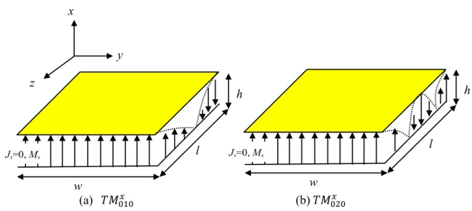
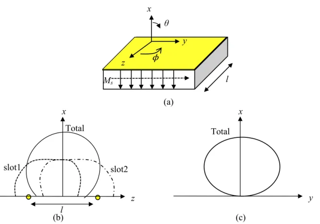
Referring to cavity model in [6], a rectangular microstrip antenna can be represented as an array of two radiating narrow apertures; patch width of w
pis separated by a distance of
lp. Charge distribution in the cavity model is explained from the formation of the fields within the cavity is explained. When the microstrip patch is excited, potential difference is formed on the top patch, feed line and bottom ground plane. Charge movement due to potential difference causes edges of the patch to radiate.
Fig. 3.1 Geometry of the proposed antenna.
x z y y
upper feed line line