Rearrangement of crystal lattice at a Ag/Ag
and Au/Au bonded interface in atomic diffusion
bonding
著者
Shigenobu Matsuda, Miyuki Uomoto, Ayaka Miura,
Takehito Shimatsu
journal or
publication title
Japanese Journal of Applied Physics
volume
59
number
SB
page range
SBBC01-1-SBBC01-3
year
2019-11-27
URL
http://hdl.handle.net/10097/00129725
doi: 10.7567/1347-4065/ab4f27Japanese Journal of Applied Physics 59, SBBC01(1-3) (2020) DOI:10.7567/1347-4065/ab4f27
1
Rearrangement of Crystal Lattice at a Ag/Ag and Au/Au Bonded Interface in
Atomic Diffusion Bonding
Shigenobu Matsuda1, Miyuki Uomoto1, Ayaka Miura1, and Takehito Shimatsu1,2,3*
1 Frontier Research Institute for Interdisciplinary Sciences (FRIS), Tohoku University, Sendai 980-8578, Japan 2 Research Institute of Electrical Communication (RIEC), Tohoku University, Sendai 980-8577, Japan 3 Center for Spintronics Research Network (CSRN), Tohoku University, Sendai 980-8577, Japan
*E-mail: [email protected]
This study examines atomic diffusion bonding (ADB) of wafers using Ag and Au films in vacuum at room temperature. Transmission electron microscopic images show remarkable crystal lattice rearrangement that occurs at depths greater than 50 nm from the connected Ag/Ag film interface. The Au/Au interface fluctuation attributable to the crystal lattice rearrangement is 5–10 nm. X-ray diffraction reveals that the crystal lattice rearrangement for Ag/Ag interface occurs remarkably at thicknesses of less than 150 nm, indicating high bonding potential when using Ag films in ADB. Large surface roughness in the thick film region probably suppresses the crystal lattice rearrangement.
Atomic diffusion bonding (ADB) of wafers is a promising process to achieve room-temperature wafer bonding1,2) along with surface-activated bonding3–6). In ADB processing, thin metal films are fabricated on two flat wafer surfaces using sputter deposition, with subsequent bonding of the two films on the wafers in vacuum. Any mirror-polished wafer can be bonded using thin metal films in the ADB process. The high atomic diffusion coefficient obtained at the film surfaces and grain boundaries, in addition to high surface energy, enables bonding at room temperature without high loading pressure. Crystal lattice rearrangement occurs at room temperature when two film surfaces mutually contact, thereby enhancing the bonding potential.
Representative material films used for ADB are Au and Ag. We bonded Si wafers in vacuum using 50-nm-thick Ag film on each side. Then the bonded interface structure of Ag/Ag films was compared to that obtained using Au films of equal film thickness.7) Images obtained using transmission electron microscopy (TEM) revealed that crystal lattice rearrangement occurred at room temperature at depths greater than 50 nm from the original film interface in Ag(50 nm)/Ag(50 nm) bonded films, although fluctuation of the Au/Au interface caused by the crystal lattice rearrangement was 5–10 nm. Results suggest a high bonding potential when using Ag film in ADB.
This study assessed ADB of wafers at room temperature using Ag films in vacuum and examined the crystal lattice rearrangement at the bonded interface of Ag/Ag films. Thereafter, we compared the results with those obtained from bonding using Au films.
Using magnetron sputter deposition, Ag films were deposited with Ta underlayers on two flat Si (001) wafer surfaces. Film thicknesses on each side, , of the Ag film were varied from 10 nm 200 nm on each side. The Ta underlayer thickness was fixed at 5 nm. Following film deposition, bonding of the two Ag films on the wafers was conducted in the same vacuum. No heating process was applied for bonding. To elucidate aspects of X-ray diffraction in the latter section of this paper, we used Ag films deposited on synthetic quartz glass wafers, without Ta underlayers. For comparison, studies using Au films were conducted using identical processes.
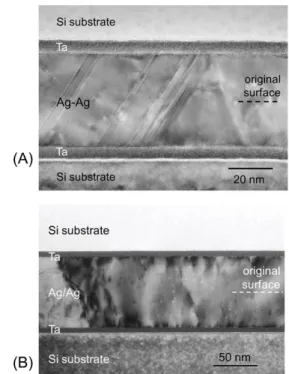
Figure 1 presents TEM cross-section image of Si wafers
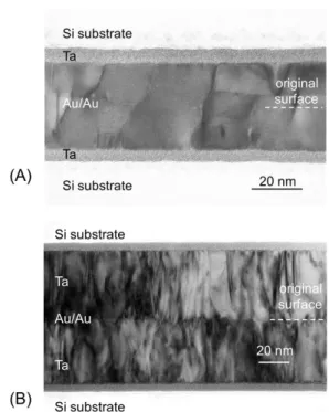
bonded using Ag films of (A) =20 nm and (B) =50 nm. Images show native Si-oxide layers as thin white layers between Ta underlayer films and Si wafers. No vacancy was observed at the bonded interface in either image because of the crystal lattice rearrangement at connected film surfaces. Many crystal grains formed over the entire film thickness even in (B), indicating that crystal lattice rearrangement occurred at room temperature at depths greater than 50 nm from the original film interface. Figure 2 presents TEM cross-section images of bonded Si wafers using Au films of (A) =20 nm and (B) =50 nm. Many crystal grains formed over the entire film thickness in (A), indicating that crystal lattice rearrangement occurred at depths greater than 20 nm from the original film interface. However, fluctuation of the Au/Au interface from the original surface caused by the crystal lattice rearrangement in (B) was 5–10 nm. Results suggest a higher bonding potential between the connected films obtained using Ag films compared to that obtained using Au films.
Fig. 1. TEM cross-section image of bonded Si wafers using Ag films of
Japanese Journal of Applied Physics 59, SBBC01(1-3) (2020) DOI:10.7567/1347-4065/ab4f27
2
Fig. 2. TEM cross-section image of bonded Si wafers using Au films of
(A) =20 nm and (B) =50 nm.
We used X-ray diffraction (XRD) to examine the crystal lattice rearrangement at the bonded interface as a function of film thickness. The Ag and Au films deposited on quartz glass wafers without Ta underlayers show weak adhesion strength of the film on wafers. Therefore, after we bonded quartz glass wafers using Ag or Au films without Ta underlayers in vacuum, we removed one side of the wafer by inserting a blade between the wafers after taking out the bonded wafers from the vacuum chamber. Figure 3(A) depicts wafers after removal for bonded Ag films of =50 nm, as examples. Wafer surfaces show mirror symmetry. Bonded Ag films remained mainly on the right-side wafer surface. Figure 3(B) presents XRD patterns for bonded Ag films of =50 nm. In the figure, an XRD pattern for 50-nm-thick single Ag film used for bonding is also shown. Here, the diffraction intensity for a single Ag film is shown as doubled. It is reasonable to infer that the difference between the XRD intensity of bonded films and double that of single film is attributable mainly to the crystal lattice rearrangement at the bonded interface. All bonded films and single films show preferred grain orientation with the fcc (111) crystal plane parallel to the film plane. The XRD intensity of the fcc (111) plane for bonded Ag films is clearly greater than double that of the single layer film, indicating that a remarkable crystal lattice rearrangement occurred at the bonded interface. This result shows good agreement with that of TEM image presented in Fig. 1(B).
Figure 4 presents XRD intensities of fcc (111) plane for bonded Ag films as a function of film thickness on each side (). In the figure, doubled intensities for single Ag films are also shown for comparison. The intensities for bonded films are greater than double those for single films at thicknesses below 150 nm, indicating that the crystal lattice rearrangement occurred remarkably in this thickness range. The ratio of intensities for bonded films
to doubled single films reached a maximum of 2.3 at 20 nm thickness, suggesting a drastic crystal lattice rearrangement at this thickness.
The behavior of bonded Au films differs from that of Ag. Figure 5 presents XRD intensities of the fcc (111) plane for bonded Au films and doubled those for single Au films as a function of film thickness on each side (). A remarkable aftereffect was observed for XRD intensities for the bonded films with =35 nm and 50 nm, with relaxation times from several hours to a few tens of hours. The nearly saturated values of intensities are plotted in the figure. The intensities for bonded films are greater than double those for single films in the thickness range below 75 nm. The maximum thickness at which remarkable crystal lattice rearrangement occurred for Au/Au bonded
Fig. 3. (A) Wafers after removal for bonded Ag films of =50 nm.
(B) XRD patterns for bonded Ag films of =50 nm. The XRD pattern for 50-nm-thick single Ag film used for bonding is also shown with doubled intensity in (B).
Fig. 4. XRD intensities of the fcc (111) plane for bonded Ag films as a function of the film thickness on each side (). In the figure, doubled intensities for single Ag films are also presented for comparison.
Japanese Journal of Applied Physics 59, SBBC01(1-3) (2020) DOI:10.7567/1347-4065/ab4f27
3
Fig. 5 XRD intensities of the fcc (111) plane for bonded Au films as a function of film thickness on each side (). In the figure, doubled intensities for single Ag films are also shown for comparison.
films is nearly half that for the bonded Ag films described above. This result supports a higher bonding potential using Ag films than that obtained using Au films. It is noteworthy that a slight increase of temperature of several tens of degrees Celsius was effective to complete the crystal lattice rearrangement for bonded films with =35 nm and 50 nm. Actually, the XRD intensities for these bonded films after 100°C annealing for 5 min were almost equal to those of the nearly saturated values shown in the figure.
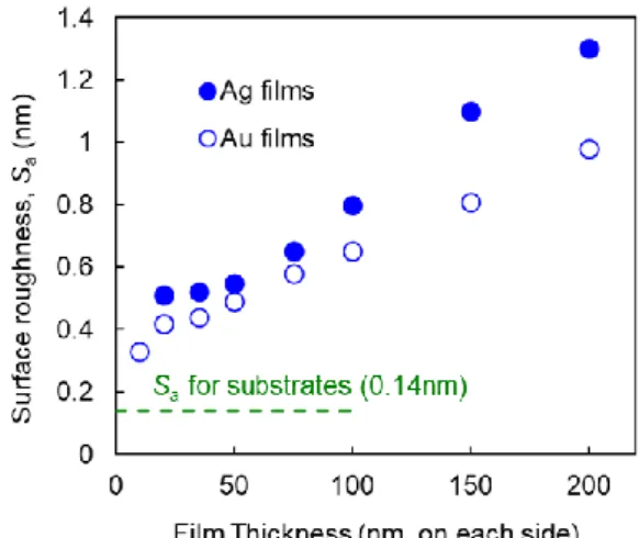
One can reasonably infer that the maximum film thickness at which a remarkable rearrangement of crystal lattice occurs between the two connected films depends on the surface roughness of the films, as is true also for ADB using the other films such as Ti8). Figure 6 portrays surface roughness Sa evaluated using atomic force microscopy (AFM) for single Ag and Au films, respectively, as a function of the film thickness. Evaluation area was 2 m× 2 m. The 5-nm-thick Ti capping films were deposited on top of Ag films before taking out Ag films from the vacuum chamber to prevent exposure of the Ag film surface to air. Sa increases as the film thickness increases in both series of films. It is likely that the increase of Sa suppresses crystal lattice rearrangement between the two connected in the thick film region. However, the values of Sa for Ag films are larger than those of Au films, particularly in the thick film region. Moreover, the value of the self-diffusion coefficient D at 300 K for Ag, as calculated from the values of the frequency factor D0 and the activation energy Q,9) is 8.3 × 10–38 m2/s, which is slightly smaller than that for Au (1.6 × 10–36 m2/s). Surface energy Es for Ag(111) is 1.25 J/m2, which is also slightly smaller than that of Au(111) (1.51 J/m2).10–12) Therefore, higher potential of crystal lattice rearrangement occurred between Ag films, compared to that between Au films, which is not explainable simply from the perspective of the differences of the values of Sa, D, and Es. Intensive efforts must be undertaken to clarify the mechanism of the crystal lattice rearrangement of connected metal films.
Fig. 6 Surface roughness Sa evaluated respectively using AFM for
single Ag and Au films as a function of film thickness.
For ADB application using Ag and Au films, the use of underlayers such as Ti and Ta is necessary to enhance the adhesion strength of Ag or Au films on wafers, yielding bonding strength greater than the fracture strength of quartz glass wafers. Moreover, the use of Ti or Ta underlayers enhanced the structural homogeneities of Ag and Au films such as (111) preferred grain orientation13) because fcc-(111) planes are the lowest surface energy crystal planes of fcc materials. It is reasonable to infer a high potential of crystal lattice rearrangement between Ag films, even on the underlayer films.
Acknowledgments
This work was supported by the Council for Science, Technology and Innovation (CSTI), Cross-ministerial Strategic Innovation Promotion Program (SIP), “Energy systems toward a decarbonized society” (Funding agency: JST).
1) T. Shimatsu and M. Uomoto, J. Vac. Sci. Technol. B 28, 706 (2010). 2) T. Shimatsu and M. Uomoto, ECS Trans. 33 [4], 61 (2010).
3) T. Suga, K. Miyazawa, and Y. Yamagata, MRS Int. Meet. Adv. Mater.
8, 257 (1989).
4) T. Suga, Y. Takahashi, H. Takagi, B. Gibbesch, and G. Elssner, Acta Metall. Mater. 40, s133 (1992).
5) H. Takagi, K. Kikuchi, R. Maeda, T. R. Chung, and T. Suga, Appl. Phys. Lett. 68, 2222 (1996).
6) E. Higurashi, T. Imamura, T. Suga, and R. Sawada, IEEE Photonics Technology Letters 19, 1994 (2007).
7) S. Matsuda, M. Uomoto, A. Miura, and T. Shimatsu, Proc. 6th Int. Workshop Low Temperature Bonding for 3D Integration, 67, (2019) [DOI: 10.23919/LTB-3D.2019.8735204]
8) T. Shimatsu and M. Uomoto, ECS Trans. 64 [5], 317 (2014). 9) The Japan Institute of Metals, Metal Data Book, p20, Maruzen,
Japan (1993).
10) L. Vitos, A.V. Ruban, H.L. Skriver, and J. Kolla´r, Surface Science
411, 186 (1998).
11) W. R. Tyson, W. A. Miller, Surf. Sci. 62, 267 (1977).
12) F. R. de Boer, R. Boom, W. C. M. Mattens, A. R. Miedema, A. K. Niessen, Cohesion in Metals, North-Holland, Amsterdam (1988). 13) O. Kitakami, S. Okamoto, and Y. Shimada, J. Appl. Phys. 79, 6880