LOW TEMPERATURE DEPOSITION OF Cu FROM
SUPERCRITICAL CARBON DIOXIDE FLUIDS USING A NOVEL
Cu(I) PRECURSOR: DEPOSITION CHARACTERISTICS AND
IMPACT ON THIN FILM STACKING
(新規Cu(I)原料を用いた超臨界流体中Cu低温堆積:堆積特性と薄膜積層への影響)
Interdisciplinary Graduate School of Medicine and Engineering
University of Yamanashi, Japan
DOCTORAL DISSERTATION
March, 2016
Presented by
MD. RASADUJJAMAN
MayT
HEU
NIVERSITY OFY
AMANASHI,J
APANAs members of the dissertation committee, we certify that we have read the dissertation prepared by
MD
.RASADUJJAMAN
entitled-LOW TEMPERATURE DEPOSITION OF Cu FROM SUPERCRITICAL CARBON DIOXIDE FLUIDS USING A NOVEL Cu(I) PRECURSOR:
DEPOSITION CHARACTERISTICS AND IMPACT ON THIN FILM STACKING (新規Cu(I)原料を用いた超臨界流体中Cu低温堆積:堆積特性と薄膜積層への影響) and recommend that it be accepted as fulfilling the dissertation requirement for the degree of Doctor of Engineering.
Prof. Eiichi Kondoh Date: 2016/03/23
Prof. Masaharu Komiyama Date: 2015/03/23
Associate Prof. Yoichi Nabetani Date: 2016/03/23
Prof. Takahiro Takei Date: 2016/03/23
Associate Prof. Masatoshi Yanagida Date: 2016/03/23
Final approval and acceptance of this dissertation is contingent upon the candidate submission of the final copies of the dissertation to the University. I hereby certify that I have read this dissertation prepared under my direction and recommend that it be accepted as fulfilling the dissertation requirement.
D
EDICATION
A
CKNOWLEDGEMENTS
I would first like to acknowledge my major advisor, Prof. Eiichi Kondoh, who believed in this project from the start and continuously motivated me to see it to fruition. Throughout my degree, he challenged me to become a more meticulous and thoughtful researcher and I am sincerely grateful for his guidance. My gratitude is extended to my committee members Prof. Masaharu Komiyama, Associate Prof. Yoichi Nabetani, Prof. Takahiro Takei, visiting Associate Prof. Masatoshi Yanagida, who have each used their expertise to guide my studies and all of whom helped me grow as a scientist. I would like to thank Professor Mikhail R. Baklanov from IMEC, Belgium for acting as an external committee member of my defense.
Thanks also to my fellow research group members, both past and present undergraduate and graduate students, specially Ueno-san, Osada-san, Teraoka-san, Goto-san, Tamekuni-san, Nakamura-san, Yamaguchi-san, Kawakami-san, Kurita-san, Suzuki-san, Segawa-san and Hayashi-san, who made working in the laboratory such a pleasant and collaborative experience. Notably, Assistant Prof. Mitsuhiro Watanabe, and Dr. Masahiro Matsubara from whom I have learned so much about the SFCD for metal deposition and for help with processing all of my tiny pieces in the laboratory. I would like to thank Dr. Yuichi Kurashima from Ubiquitous MEMS and Micro Engineering R.C. laboratory, AIST, Tsukuba for his guidance and assistance with electroplating and lithography process that I have learned during my internship. For financial support during my doctoral research, I greatly acknowledge the Green Energy Conversion Science and Technology Program, University of Yamanashi, Japan. This project would not have been possible without their generous funding.
I would like to express my deepest gratitude to my parent in Kurigram, Bangladesh, for their unconditional love and devoted support. Their endless encouragement is unforgettable. To all my other family members and friends, thank you for lending a listening ear and being supportive even when you did not completely understand what I was talking about.
Lastly, I would like to recognize the unwavering love and support of my wife, Liza. She rejoiced in my successes, consoled me in my failures, and never let me lose sight of the bigger picture. She were always with me and made me feel comfort at home. I want to share this honorable moment with her and our loving son Musad forever....
A
BSTRACT
The packing density of microelectronic devices has increased exponentially over the past decades. There has been an increasing interest in the deposition of Cu thin films using chemistry-based methods to meet the requirements of the continuous scaling down of electronic devices for the manufacturing of highly integrated microelectronic devices. Supercritical fluid chemical deposition (SFCD) is a demonstrated technology in a laboratory scale, which is the reduction of organometallic compounds with hydrogen in supercritical carbon dioxide (scCO2). ScCO2 is emerging as a viable and environmentally sustainable platform due to its tunable solvent properties combined with low surface tension and viscosity, which allow depositing thin conformal films, filling deep trenches with high-aspect-ratios, etching, and cleaning thin insulator. This process have the potential to build future generations of microelectronic devices with higher speeds and longer lifetimes. According to the latest version of the International Technology Roadmap for Semiconductors (ITRS), suggested techniques to replace sputtering is SFCD.
The main objective of the research presented in this dissertation is to benefit advanced SFCD technology from its current state of being an established laboratory technology, to a point where it is a feasible manufacturing option for the miniature- ization of integrated circuits in microelectronic industry. There are several milestones for Cu-SFCD realization. The challenges that must be overcome in order to meet this goal for industrialization includes low temperature deposition, filling high aspect ratio features, alloy deposition and some reliability issue which includes adhesion. In order to complement SFCD technology for scale-up, an understanding of the deposition mechanism and resolution of reliability issues such as interfacial film adhesion must be resolved. In addition, to advance the utility of scCO2 fluid, a more thorough understanding of surface chemistry for a novel metal etching and cleaning at high pressures is needed.
Low temperature decomposable precursor for Cu is necessary in order to convert a bench top result into a practical application for industrial use. To do this, it is critical to have a fundamental understanding of the mechanism or chemistry behind the reaction process in SFCD. For this purpose, in this dissertation, a detailed mechanism of Cu deposition is carried out using a novel Cu(I) precursor such that growth rate
orders and a mechanism can be established together with a deep nanotrench filling ability. This will help enable control over the reaction by promoting predictive kinetic results and will allow for an overall optimization of the process.
Reliability is of the utmost importance for fabricated devices if they are to survive the upcoming severe steps in the fabrication process as well as perform and last under standard and extreme usage conditions. The challenge of reliability is accessed by addressing the adhesion of the metallization layers deposited by SFCD. A quantitative determination of the interfacial adhesion of as deposited and pretreated metallization layers from SFCD onto barrier layers is used to determine the reliability of these films for industry standards.
Extension of SFCD technology to a variety of commercially oriented applications is important in order to show the techniques versatility. Extension of the basics of SFCD by performing codeposition or alloy deposition, stacking thin films for device fabrication and integration with other unique technologies for novel applications demonstrates the ability of this technique to satisfy a wide range of commercial applications and be used as the basis for new technologies.
In this dissertation, therefore started with the codeposition of Cu and Ni thin films from a mixed Cu precursor [Cu(II)(hfac)2 for Cu and Ni(II)(hfac)2 for Ni] in scCO2 solutions to gain a general understanding of alloy deposition in a supercritical medium as well as the interdiffusion between Cu and Ni (Chapter 2). A Cu/Ni bilayer was formed where Cu deposited first, and then Ni, with no attempt to control interdiffusion. It was found that SFCD Cu diffused rapidly to form a solid solution with the Ni seed layer, resulting in poor adhesion (45.5 mN) determined with a microscaratch tester. This was because the deposition temperature was too high, and Cu and Ni diffuse too rapidly above 350°C. Also, Cu(II)(hfac)2 and Ni(II)(hfac)2 precursors were used, both of which contain fluorine and oxygen. Therefore, to suppress excessive diffusion, the deposition temperature must be reduced.
Therefore, a non-fluorinated novel Cu(I) amidinate precursor, [Cu(DIPPA)]2, was employed to reduce the deposition temperatures and was studied the SFCD of Cu filling in Ru- and TiN-lined deep nanotrenches (Chapter 3). The Cu(I) amidinate precursor dispersed well in an acetone/CO2 solution with molecular hydrogen as the reducing agent at very low temperatures. High-purity Cu films were grown on both Ru and TiN substrates at a lower deposition temperature (140°C) than typical temperatures reported for Cu(II)(hfac) and Cu(II)(dibm) precursors. On the Ru
surface, Cu nucleated densely, forming smooth, strongly adherent films. At 140°C, the excellent filling capability of Cu in Ru- or TiN-lined nanotrenches was demonstrated. The deposition mechanism of Cu in scCO2 by H2 reduction of [Cu(DIPPA)]2, were studied using a flow type system with a stainless steel reactor, at 15 MPa pressure (Chapter 4). The low deposition temperature of about 140°C was needed to start for film growth as mention in chapter 3, but using a batch-type system and the obtained films exhibited a smooth surface with a measured roughness equivalent to that of the substrate on which they were deposited. Films were deposited at substrate temperatures from 140 to 240°C. From the temperature dependence of the growth rate, the average activation energy for Cu growth was determined at 0.20±0.03 eV. The dependences of the growth rate on the precursor concentration, H2 concentrations were studied. A mechanism based on dissociative adsorption of precursor and hydrogen concentration at vacant surface sites was proposed. A Langmuir– Hinshelwood type growth mechanism was discussed, and a rate equation for growth was proposed.
The low-temperature deposition of Cu on a Ni-lined substrate in scCO2 have been studied using [Cu(DIPPA)]2 (Chapter 5), to fabricate the Cu/Ni stack again. The films and interfaces were characterized by Auger electron spectroscopy. At a low temperature (140°C), a Cu/Ni stack with a sharp Cu/Ni interface was successfully deposited. The stack had a high adhesion strength (>1000 mN) according to microscratch testing. The high adhesion strength originated from strong interfacial bonding between the Cu and the Ni.
Finally, SFCD technique has been employed to etch transition metal (Cu, Ni, Co, and Fe) thin films in scCO2. The metals were removed by reacting with a chelating agent, hexafluoroacetylacetone, by dissolving the reaction product compounds in scCO2. The operating temperatures were 100−250°C and pressure was fixed at 10 MPa. The changes in the optical transmittance and thickness of the films indicated etching in the scCO2. Scanning electron microscope observation and surface probe microscope analysis confirmed that there was no significant film agglomeration, in particular, and that the Fe and Co films were uniformly etched. This process is potentially applicable to the etching of metal thin films for magnetoresistive memory processing.
T
ABLE
OF
C
ONTENTS
T
ITLEP
AGE………...iD
EDICATION………...iiiA
CKNOWLEDGEMENTS………...ivA
BSTRACT………...vT
ABLE OFC
ONTENTS………...viiiL
IST OFF
IGURES………...xiL
IST OFT
ABLES………...xv 1 INTRODUCTION... 1 1.1 Background ... 2 1.1.1 Overview ... 21.1.2 Cu-based interconnect for ULSIs/packaging ... 3
1.2 Methods of thin film formation... 5
1.2.1 Conventional deposition methods ... 5
1.3 Thin film deposition using supercritical fluid as a medium ... 9
1.3.1 Overview ... 9
1.3.2 Supercritical CO2 as a solvent for thin film deposition ... 12
1.3.3 Metal film deposition in scCO2 ... 13
1.4 Review of SFCD metal thin films ... 14
1.5 Cu/Ni alloy deposition and stack formation ... 19
1.6 Precursors for Cu-SFCD ... 21
1.7 SFCD reaction system... 25
1.7.1 Batch type reaction system ... 26
1.7.2 Flow type reaction system ... 27
1.8 Thesis outline ... 29
1.9 References ... 31
2 CODEPOSITION OF Cu/Ni THIN FILMS FROM MIXED PRECURSOR IN SUPERCRITICAL CARBON DIOXIDE ... 37
2.1 Introduction ... 38
2.2 Experimental method and materials... 39
2.2.1 Materials and procedure ... 39
2.2.2 Experimental tools ... 39
2.3 Results and discussion ... 39
2.5 References ... 49
3 SUPERCRITICAL FLUID CHEMICAL DEPOSITION OF Cu IN Ru AND TiN-LINED DEEP NANOTRENCHES USING A NOVEL Cu(I) AMIDINATE PRECURSOR ... 51
3.1 Introduction ... 52
3.2 Experimental method and materials... 52
3.2.1 Materials and procedure ... 52
3.2.2 Experimental tools ... 53
3.3 Results and discussion ... 53
3.3.1 Solubility of Cu(I) amidinate precursor ... 53
3.3.2 Deposition characteristics of Cu ... 54
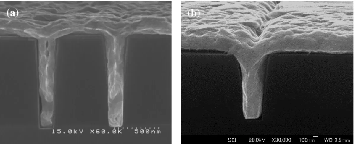
3.3.3 Filling of Ru-lined nanotrenches with Cu ... 60
3.3.4 Filling of TiN-lined nanotrenches with Cu ... 61
3.4 Conclusions ... 62
3.5 References ... 63
4 COPPER THIN FILM GROWTH USING Cu(I) AMIDINATE PRECURSOR IN SUPERCRITICAL CARBON DIOXIDE: DEPOSITION KINETICS ... 65
4.1 Introduction ... 66
4.2 Experimental method and materials... 67
4.2.1 Procedure ... 67
4.2.2 Materials ... 68
4.2.3 Experimental tools ... 68
4.3 Results and discussion ... 68
4.3.1 Film quality ... 68
4.3.2 Temperature dependence ... 71
4.3.3 Precursor concentration dependence... 74
4.3.4 Hydrogen concentration dependence ... 75
4.3.5 Reaction pressure dependence ... 76
4.3.6 Reaction orders and mechanism ... 77
4.4 Conclusions ... 81
4.5 References ... 82
5 FABRICATION OF A Cu/Ni STACK IN SUPERCRITICAL CARBON DIOXIDE AT LOW-TEMPERATURE ... 84
5.1 Introduction ... 85
5.2.1 Procedure and materials ... 86
5.2.2 Experimental tools ... 86
5.3 Results and discussion ... 86
5.3.1 Basic deposition characteristics ... 86
5.3.2 Surface morphology ... 87
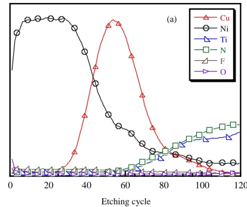
5.3.3 AES depth profile of the Cu/Ni stack ... 88
5.3.4 Adhesion strength of the Cu/Ni stack ... 91
5.4 Conclusions ... 92
5.5 References ... 93
6 SUPERCRITICAL CARBON DIOXIDE ETCHING OF TRANSITION METAL (Cu, Ni, Co, Fe) THIN FILMS ... 95
6.1 Introduction ... 96
6.2 Experimental methods and materials ... 97
6.3 Results ... 98
6.3.1 Feasibility studies... 98
6.3.2 Etching behavior in scCO2 ... 100
6.4 Discussion ... 105
6.4.1 Etching chemistry ... 105
6.4.2 Surface roughening and metal removal ... 106
6.5 Conclusions ... 109
6.6 References ... 110
7 CONCLUSIONS AND FUTURE WORK ... 112
7.1 Conclusions ... 112
7.1.1 Codeposition of Cu/Ni and alloy formation... 112
7.1.2 Cu-Filling in nanotrenches using a novel Cu(I) precursor... 112
7.1.3 Deposition mechanism of Cu film using a novel Cu(I) precursor ... 113
7.1.4 Cu/Ni stack formation ... 113
7.1.5 Transition metal etching ... 113
7.2 Future work ... 114
7.2.1 Codeposition and adhesion strength ... 114
7.2.2 Novel metal and metal alloy etching ... 114
APPENDICES ... 115
A. Publications ... 115
L
ISTS OFF
IGURESFigure Page
Fig. 1.1 Moore’s Law states that the number of transistors per die will double every 18-24 months [4].………..……….…..4 Fig. 1.2 Cross-section of a transistor (top) and metal interconnects (bottom) in recent generations of processors [5]...……….4 Fig. 1.3 Properties of supercritical fluid systems. (a) Density of CO2 as a function of pressure for isotherms at 40, 80, and 120°C [26]. (b) Surface tension of water, hexane, and liquid carbon dioxide as a function of temperature at saturation [26]. Surface tension for all fluids vanishes at the critical points.………...…………..11 Fig. 1.4 Phase diagram of CO2.………..…….……….12 Fig. 1.5 Deposition mechanism of metal film formation in supercritical fluid.……...13 Fig. 1.6 Phase diagram of Cu-Ni alloy system.………...20 Fig. 1.7 Chemical structures of Cu(II) and Cu(I) precursors for CVD and SFCD application...23 Fig. 1.8 (a) Chemical structure of Cu(I) precursor, diisopropylpropion-amidinate
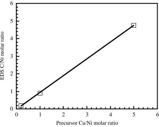
(DIPPA) Cu(I) dimer, [Cu(DIPPA)]2, and (b) appearance of Cu(I) precursor………...…..24 Fig. 1.9 Internal views of (a) batch and (b) flow reaction systems…...26 Fig. 1.10 Schematic diagram of the batch-type SFCD reaction system...27 Fig. 1.11 Schematic diagram of the flow-type supercritical fluid chemical deposition system...28 Fig. 2.1 (a) AES depth profiles of a Cu-Ni film with precursor compositions of 1:1..41 Fig. 2.1 (b) AES depth profiles of a Cu-Ni film with precursor compositions of 5:1..41 Fig. 2.1 (c) AES depth profiles of a Cu-Ni film with precursor compositions of 1:5..42 Fig. 2.2 EDS Cu/Ni molar ratios of films with different precursor Cu/Ni molar.…....42 Fig. 2.3 AES depth profiles of ex situ annealed (at 300 ºC for 30 min) Cu-Ni film .with a precursor composition of 1:1.………..…...………43
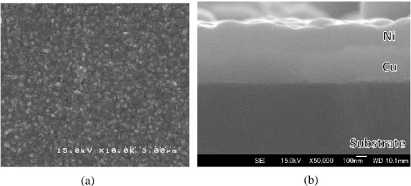
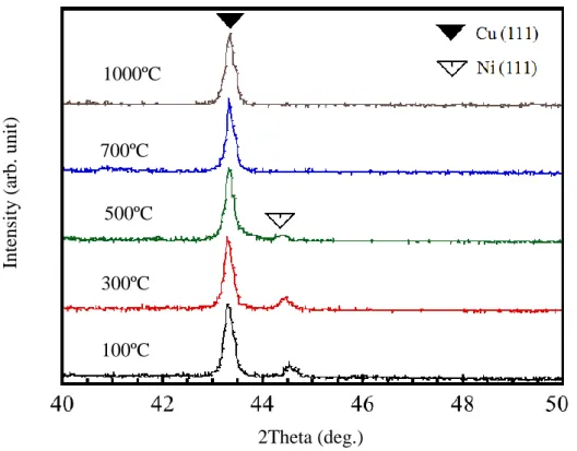
Fig. 2.4 (a) Surface and (b) cross-sectional SEM images of Cu-Ni films with a precursor composition of 1:1. The deposition temperature was 240ºC ...43 Fig. 2.5 Ex situ X-ray diffraction patterns of a Cu-Ni film with a precursor composition of 1:1 at different temperatures.………...………..44 Fig. 2.6 (a) In situ X-ray diffraction patterns of a Cu-Ni film with a precursor composition of 1:1 at different vacuum annealing temperatures.……..……45 Fig. 2.6 (b) Intensity ratios between Cu (111) and Ni (111) peaks estimated from
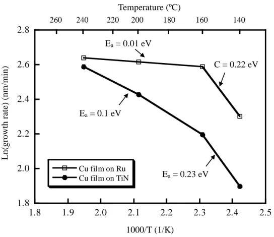
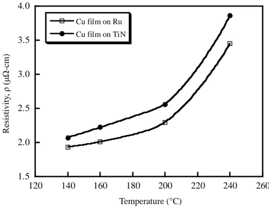
(a)………46 Fig. 2.7 SEM images of 250-nm-wide trenches filled with (a) Cu-Ni at a precursor composition of 1:1 and (b) only Cu at a deposition temperature of 200ºC....47 Fig. 3.1 Solubility of [Cu(DIPPA)]2 in common organic solvents.………..54 Fig. 3.2 Arrhenius plot of Cu deposition from scCO2 fluids on Ru and TiN…….…..55 Fig. 3.3 Resistivity of Cu films on Ru and TiN substrates as a function of deposition
temperature.………..………..56 Fig. 3.4 (a) Cross-sectional SEM image and (b) EDS maps of the Cu film deposited at 240°C on the Ru substrate.………..………...57 Fig. 3.5 AES depth profiles of Cu films deposited at (a) 140 and (b) 240°C on the TiN substrate.…………..………...58 Fig. 3.6 X-ray diffraction patterns of Cu films deposited at different deposition temperatures.…..………59 Fig. 3.7 Adhesion of Cu films deposited on the TiN substrate at different deposition
temperatures.…..………60 Fig. 3.8 Cross-sectional SEM images of Cu films deposited in Ru-lined nanotrenches
at (a) 140 (b) 160 and (c) 240°C. The nominal dimension is defined as the trench width at the opening. The magnification is the same in all micrographs………61 Fig. 3.9 Cross-sectional SEM images of Cu films deposited in TiN-lined nanotrenches using the [Cu(DIPPA)]2 precursor at 140°C. The nominal dimension is defined as the trench width at the opening. The magnification is the same in all micrographs………..…….61 Fig. 4.1 AES depth profiles of a Cu films deposited at 180°C on a Ta coated SiO2
substrate.…..………..69 Fig. 4.2 Field emission scanning electron microscopy of Cu film deposited by SFCD
at hydrogen concentrations of (a) 6.65% (b) 4.65%and (c) 2.66%. Reaction conditions: 180°C, 15 MPa, 35.5% [Cu(DIPPA)]2, 60 min deposition……..70
Fig. 4.3 Scanning probe microscopy image of a Cu film deposited by SFCD, (a) 140°C (surface roughness is 4.2 nm for a Cu film thickness of 55 nm) and (b) 200°C (surface roughness is 7.6 nm for a Cu film thickness of 110 nm). Reaction conditions: 15 MPa, 3.53 × 10⁻³ [Cu(DIPPA)]2, 6.65% hydrogen, 60 min deposition……….………...71 Fig. 4.4 Arrhenius plots of deposition rate as a function of H2 concentration. The
concentration of precursor fixed at 3.53 × 10⁻³.……….………73 Fig. 4.5 Cu film deposition rate dependence on [Cu(DIPPA)]2 concentrations. Reaction conditions: 140°C, 15 MPa, 6.65% hydrogen, 60 min deposition. Zero order kinetics is observed at high precursor concentrations. Line is a fit to a Langmuir-Hinshelwood rate equation.….………...74 Fig. 4.6 Cu film deposition rate dependence on hydrogen concentrations. Reaction conditions: 140°C, 3.53 × 10⁻³ [Cu(DIPPA)]2, 15 MPa, 60 min deposition. Using differential kinetics, zero order kinetics is observed at higher hydrogen concentrations. Line is a fit to a Langmuir-Hinshelwood rate equation …...75 Fig. 4.7 Cu film deposition rate dependence on reaction pressure. Reaction conditions:
180°C, 8-15 MPa, 3.53 × 10⁻³ [Cu(DIPPA)]
2, 6.65% hydrogen, 60 min deposition. Pressure does not influence growth rate over the range of 12-15 MPa.………...76 Fig. 4.8 Schematic reaction mechanism for Cu SFCD in the [Cu(DIPPA)]2/H2 system……….………...79 Fig. 5.1 Arrhenius plot of Cu deposition rate on Ni films. The deposition time was
fixed at 15 min.………..……….87 Fig. 5.2 Scanning electron micrographs of Cu/Ni stacks prepared at Cu deposition temperatures of (a) 140 (b) 200 (c) 240 and (d) 280°C. The deposition time was fixed at 15 min.……….………..88 Fig. 5.3 (a) AES depth profiles for Cu/Ni stacks prepared at Cu deposition
temperatures of 140°C. The deposition time was 15 min.………..…...89 Fig. 5.3 (b) AES depth profiles for Cu/Ni stacks prepared at Cu deposition
temperatures of 200°C. The deposition time was 15 min..………89 Fig. 5.3 (c) AES depth profiles for Cu/Ni stacks prepared at Cu deposition
temperatures of 240°C. The deposition time was 15 min………..…………90 Fig. 5.3 (d) AES depth profiles for Cu/Ni stacks prepared at Cu deposition
temperatures of 280°C. The deposition time was 15 min………..90 Fig. 6.1 Schematic diagram of supercritical CO2 etching apparatus.………..98
Fig. 6.2 Typical digital camera photographs of a Co film (a) before and (b) after etching. ……….………...…..99 Fig. 6.3 Transmittance of the metal film as a function of etching temperature.……100 Fig. 6.4 Remaining metal film layer thickness vs. temperature of etching with Hhfac.
The concentration of Hhfac and etching time were fixed at 3.5 × 10⁻³ mol and 60 min, respectively.………….………101 Fig. 6.5 Remaining metal film layer thickness vs. time of etching with Hhfac. The concentration of Hhfac was fixed at 3.5 × 10⁻³ mol. The temperature was fixed at 200°C for Cu and Ni and 125°C for Fe.………..……...….102 Fig. 6.6 Surface roughness of metal films as a function of temperature.…………...102 Fig. 6.7 SEM images of Cu film surfaces (a) before and after etching at (b) 100°C, (c) 200°C, and (d) 200°C.……….………103 Fig. 6.8 SEM images of Co film surfaces (a) before etching and after etching at (b)
150°C, (c) 200°C, and (d) 250°C.………..…..………104 Fig. 6.9 Schematic diagram of the etching behavior of Cu films...107 Fig. 6.10 Schematic diagram of the etching behavior of Co films.………108
L
ISTS OF TABLESTable Page
Table 1.1 Resistivity of selected metals.………3
Table 1.2 Comparison between Al and Cu………...3
Table 1.3 Comparison of selected properties of supercritical fluids to those of liquids and gases [26].…………...……….………..10
Table 1.4 Critical parameters of selected solvent systems [26]...13
Table 1.5 Summary of metal films deposited by supercritical fluid deposition and their Deposition conditions...15
Table 1.6 Physical properties of Cu(II) and a novel Cu(I) amidinate precursor...24
Table 4.1 Experimental conditions employed in this study...68
Table 4.2 Activation energies of Cu film deposition...73
Table 4.3 Kinetic data for selected Cu(I) and Cu(II) chemistries...73
Table 5.1 Adhesion strength of Cu/Ni stacks formed at different deposition temperatures. The deposition time was 15 min.…...…….…………...91
CHAPTER 1
1 INTRODUCTION
This chapter serves as an introduction to this thesis. First, current state-of-the-art Cu-interconnects technology and some of its limitations are discussed. This is followed by a discussion on supercritical fluid chemical deposition (SFCD), which has been identified as a potential solution to many problems in current interconnect technology. Challenges in the conventional deposition are identified, and SFCD deposition are presented as potential deposition technique to solve this challenges. Requirements of successful integration of SFCD into ULSI technology and overview of previous work which include thin metal film deposition by SFCD, review of SFCD metal thin films, SFCD Cu precursors, Cu/Ni stack formation are presented. Lastly, two basic SFCD reaction systems and outline of the thesis are presented.
1.1 Background
1.1.1 Overview
The main objective of the research presented in this dissertation is to benefit advanced SFCD technology from its current state of being an established laboratory technology, to a point where it is a feasible manufacturing option for the miniaturization of integrated circuits in microelectronic industry. In microelectronic industry, there are several milestones for Cu-SFCD realization. The challenges that must be overcome in order to meet this goal for industrialization includes low temperature deposition, filling high aspect ratio features, alloy deposition and some reliability issues which include the adhesion.
Low temperature decomposable precursor for Cu is necessary in order to convert a bench top result into a practical application for industrial use. To do this, it is critical to have a fundamental understanding of the mechanism or chemistry behind the reaction process in SFCD. For this purpose, in this dissertation, a detailed mechanism of Cu deposition is carried out using a novel Cu(I) precursor such that growth rate orders and a mechanism can be established together with a deep nanotrench filling ability. This will help enable control over the reaction by promoting predictive kinetic results and will allow for an overall optimization of the process.
Reliability is of the utmost importance for fabricating devices if they are to survive the upcoming severe steps in the fabrication process as well as perform and last under standard and extreme usage conditions. The challenge of reliability is accessed by addressing the adhesion of the metallization layers deposited by SFCD. A quantitative determination of the interfacial adhesion of as deposited and pretreated metallization layers from SFCD onto barrier layers is used to determine the reliability of these films to meet industry standards.
Extension of SFCD technology to a variety of commercially oriented applications is important in order to show the techniques versatility. Extension of the basics of SFCD by performing co-deposition or alloy deposition, stacking thin films for device fabrication and integration with other unique technologies for novel applications demonstrates the ability of this technique to satisfy a wide range of commercial applications and be used as the basis for new technologies.
1.1.2 Cu-based interconnect for ULSIs/packaging
Aluminum (Al) and its alloys have been replaced by copper (Cu) for ULSIs or packaging interconnection due to its low resistivity (1.69 μΩ-cm, Table 1.1) and better reliability against electromigration (Table 1.2) [1,2]. Highest performance is achieved when copper and low-k dielectrics are combined, as evidenced by the industry trend. However, Copper-based interconnect of ULSIs circuits has become an area of intense research interest as devices are scaled down in order to increase circuit density.
Table 1.1 Resistivity of selected metals.
Metal Bulk resistivity (μΩ-cm)
Ag 1.63
Cu 1.67
Au 2.35
Al 2.67
W 5.65
Table 1.2 Comparison between Al and Cu.
Properties Al Cu
Melting point 660°C 1083°C
Activation energy for lattice diffusion 1.4 eV 2.2 eV Activation energy for lattice diffusion 0.4 – 0.8 eV 0.7 – 1.2
In the past decades, microelectronics have developed along with a constant speed of scaling to maximize transistor density due to the requirements of electrical and functional performances [3]. In 1965, as predicted by a cofounder and former CEO of Intel, Gordon Moore, new technology generations have been introduced with a 2-year cycle, and packing density and device speed have increased exponentially at rapidly decreasing cost per function (Fig. 1.1) [4]. Followed with, 90 nm in 2003, 65 nm in 2005, 32 nm in 2009, 22 nm in 2011, Intel began high volume production with its 14 nm process technology with second-generation tri-gate gate transistors with 42 nm minimum pitch since late 2013, where minimum interconnect pitch 52 nm (0.65x) was adopted as shown in Fig. 1.2 [5]. The 10 nm process is on track for production in 2018. With breakthrough 10 nm process technology, one can expect faster processing speeds, greater computing capability, and improved functionality.
Fig. 1.1 Moore’s Law states that the number of transistors per die will double every 18-24 months [4].
Fig. 1.2 Cross-section of a transistor (top) and metal interconnects (bottom) in recent generations of processors [5].
However, International Technology Roadmap for Semiconductors (ITRS) predicts microprocessors will enter production at the 1.8 nm technology node by 2025 the [6]. Therefore, in ULSIs, the interconnect dimensions are continuously being downscaled and aspect ratios are increasing and reliability becomes more of an issue. Interconnect
Interconnect pitch 80 nm 22 nm process 2011 14 nm process 2013 Transistor (42 nm Fin Pitch) Interconnect pitch 52 nm Transistor (60 nm Fin Pitch) 42nm 60nm
metallization generally requires good conductivity, electromigration resistance, controllable contact performance, adherence, thermal stability, ability to be patterned into a desirable geometry and filling high-aspect-ratio features, and economic feasibility. However, defect free deposition of Cu and other materials within high aspect ratio features at these dimensions poses a formidable challenge. Other requirements include good uniformity with low impurity and lower growth temperatures [7]. Good material properties with minimum damage to the substrate materials are also needed. Furthermore, environmental regulations are becoming stricter in the coating industry [8].
There are major challenges in the implementation of Cu in ULSIs or packaging devices. Copper is not compatible with some of the other materials used in ICs. For example, copper weakly adhere to dielectric substrates or silicon substrates under the high temperatures being reached in device manufacture. Additionally, in the standard damascene metallization procedure, Cu needs to be filled in a high aspect ratio features. Confronting these challenges requires three things: finding a method and a suitable precursor for low temperature deposition, patterning the Cu, and finding a way to improve the adhesion of copper on substrate.
1.2 Methods of thin film formation
1.2.1 Conventional deposition methods
Along with the rise of micro- and nanofabrication with increasing complexity and decreasing dimensions is placing stringent requirements on the deposition of metal thin films or nanostructures. These requirements include the conformal coverage of complex topographies, complete filling of narrow high aspect ratio features, reduction in process temperatures, and reduction of waste from current processing technologies. Several current deposition techniques have explored to fabricate thin film. The most common conventional deposition techniques for thin film are physical vapor deposition (PVD), atomic layer deposition (ALD), chemical vapor deposition (CVD), and electrochemical deposition (ECD) that include both liquid- and vapor-phase techniques. PVD, ALD and CVD are gas phase techniques while ECD is liquid phase techniques. In this study, metal thin film has been deposited by supercritical fluid chemical deposition (SFCD).
Physical Vapor Deposition
Physical Vapor Deposition (PVD) is a collective set of processes used to deposit a thin solid layers of materials, typically in a low-pressure environment. The two physically based methods for depositing thin films are evaporation and sputtering. They are called physical vapor deposition processes because these techniques do not involve chemical reactions. The vapors of the material to be deposited are produced either by heating or by energetic ion bombardment.
Evaporation is the oldest technique for the physical vopor deposition of thin films, such as Au and Al. The metal layers for all of the early generations of semiconductor technologies were deposited by evaporation. In an evaporator, the wafers are loaded into a high-vacuum chamber that is commonly pumped with a cryopump. The material to be deposited is loaded into a crucible and is heated by an embedded resistance heater and an external power supply. Since the pressure inside the chamber is very low (< 10-5 Torr), vapors of the material travel across the chamber in a straight line until they strike the substrate surface, where they accumulate and form a film [9]. A mechanical shutter is typically used in front of the container to start and stop the deposition abruptly. Evaporation only allows for a line of sight deposition, also known as shadowing, which limits its use to planar substrates and low aspect ratio structures. Line of sight limitations for most PVD techniques present difficulties when conformal deposition within high aspect ratio features is needed. In addition, creating thick films is problematic due to the limited size of targets as constrained by the limitations imposed by heat transfer of the heating filaments.
Sputtering, a more popular PVD technique, occurs when a target is bombarded with energetic ions, typically Ar+. The atoms at the surface of the target are dislodged and then transported to the substrate, where the deposition occurs. It has the ability to achieve better step coverage and to produce well-controlled layers of compound materials and alloys than evaporation techniques. In a sputtering system, the plasma chamber is arranged so that high-energy ions strike the target that contains the material to be deposited. Because of the higher pressure (~10-3 Torr) in sputtering systems, the atoms experience more gas-phase collisions and produce films with higher conformality. Due to the physical nature of the process, sputtering can be used to deposit a wide variety of materials. DC sputtering is usually favored while depositing elemental metals due to its high sputter rates. RF plasma is used to deposit insulting materials such as SiO [9]. Sputtering is now the primary technique used to
deposit diffusion barrier (TaN, TiN), adhesion layer (Ta, Ti), and seed layer (Cu) in copper interconnect systems. The advantage of PVD is the deposition of alloys which is as simple as making the target the same composition as the film desired. This process can also be used in the reverse manner, called sputter etching. This is used to clean substrates prior to film deposition.
Electron beam (E-beam) deposition is similar to evaporation; however, instead of increasing the temperature of the target with a filament, the temperature of the target is increased by an electron beam with energy up to 15 keV. This allows for the evaporation of the target and then deposits a thin film on the surface of the substrate. E-beam is cleaner and can deposit more versatile materials.
Chemical Vapor Deposition
Although most metal films for ULSIs are deposited using PVD methods, they have major problems associated with step coverage. This is a particular concern with future technologies where very small, high aspect ratio features require conformal step coverage. Chemical vapor deposition (CVD) has the best ability to achieve conformal step coverage and produces the least substrate damage.
Chemical vapor deposition is the process by which the thermal decomposition or reaction of gaseous compounds forms a thin film on the surface of a substrate. This process deposits the desired material directly from the gas phase onto the substrate in a non-line of sight deposition. Due to the high temperatures required for this process in addition to the non line of sight process, exceptional step coverage can be achieved, in principle, for even the most complex geometries. In practice, however, it is often limited by precursor vapor pressure requirments and mass-transfer-limited kinetics that preclude uniform filling of high aspect-ratio features. In addition high deposition temperatures inherent to CVD can lead to the generation of thermal-mechanical stress during device fabrication. Moreover, the requirement of high precursor volatility often dictates the use of fluorinated ligands or toxic carbonyl compounds that can generate undesireable effluents [10,11]. Fortunately, the development of plasma CVD and metallorganic CVD partially offsets this problem. The other disadvantage is that pure films can be difficult to obtain by CVD because many side reactions occur, especially in metal-organic CVD. This problem can be controlled by depositing film under optimized conditions. However, this process is used for a wide range of metals including, but not limited to, Mo, Ti, W, Ru, Cu, Pt, Pd and many more [12−17].
Atomic Layer Deposition
Atomic layer deposition (ALD) has emerged as an important technique for depositing thin films for a variety of applications [18]. ALD is similar to CVD in that it is a gas phase deposition process but at very low concentrations and is repeated numerous times. It requires alternating precursor gas exposure for self-limited reactions to form films. However, the films deposited have precise composition, conformal coverage, exceptionally high interfacial adhesion and thickness control on the angstrom level. ALD, although a candidate for conformal films with precise composition control, is only an effective solution at thicknesses of 10 nm or less due to the amount of time required to deposit the films. For thicker films, significantly longer processing times are required, thus making it unsuitable for industrial integration.
Electroplating
Electropating is a liquid phase process and currently employed for the deposition of metal films offering distinct advantages and limitations. Liquid-phase processes exhibit several limitations, including contamination issues, poor mass transport, requirement for a conducting metal layer for deposition to take place, and difficulties such as pattern collapse for the smallest device due to capillary forces. Electropating techniques such as electroless deposition offer low temperature operation and a wide-range of suitable, inexpensive precursors. Mass transfer within the liquid phase however is sluggish, and can lead to poor control over the deposition process. Moreover, surface tension prevents uniform deposition in tortuous environments, and poor miscibility with hydrogen and other gas phase reducing agents necessitates the use of toxic liquid reductants such as formaldehyde and sodium hypophosphite. Finally, electroless deposition generates large volumes of wastewater derived from plating and rinse baths that are subject to strict environmental regulations.
Electroplating is a two-step method. It requires a seed layer deposition preceding the plating fill step to insure a low-resistance conductor for the plating current and to assist in the film nucleation. This process can be used to deposit films that are very conformal. With electroplating, high precursor concentrations can be achieved due to the liquid phase of the system. However, slow mass transport in the fluid phase and large volumes of waste water and byproducts negatively influence this process.
Therefore, new processes for thin film formation have therefore been developed to address the limitations of conventional deposition techniques. Among these new
processes, those based on the use of supercritical fluids (SCFs) attracted much interest in the early 1990s, and have thereafter been extensively used for materials synthesis, [11,19,20] taking benefit of their unique properties. Indeed, while the environmental advantages of SCFs such as carbon dioxide or water are attractive, their physicochemical properties are enabling and have ultimately driven their use in thin film formation and chemical reactivity. In particular, the absence of surface tension, favorable transport properties, and densities that approach those of liquids provide means for solution-based processes in an environment that behaves much like a gas.
1.3 Thin film deposition using supercritical fluid as a medium
1.3.1 Overview
The supercritical fluid (SFCs) is simply a substance heated and compressed beyond its critical temperature (Tc) and pressure (Pc) [21]. However, a fluid is said to be supercritical, when its pressure and temperature exceed their respective critical value Tc and Pc. SFCs was used actively from late 19th century in various fields [22]. Recently, SCFs have been successfully applied in chemical processing and are now of considerable interest in applying to microelectronics [7].
A novel chemical route in thin film formation that can be obtained through a chemical reaction of a precursor or a mixture of precursors dissolved in a supercritical fluid solution [23]. This technique is so called supercritical fluid chemical deposition, frequently abbreviated SFCD or SCFD or SCF or CFD [24,25,7]. In this dissertation, it is referred to as SFCD. Using SCFs to deposit metals and metal oxides thin film on surfaces has been attracting increased attention due to the attractive properties of supercritical fluids.
Density characteristics of a SCF is between that of a gas and a liquid, but closer to that of a liquid. In supercritical region, density of a SCF increases with increased pressure (at constant temperature). When pressure is constant, density of the fluid decreases with increasing temperature [Fig. 1.3]. The dissolving effect of a SCF is dependent on its density states. SCFs are better carriers than gas to their higher density. Therefore, density is an essential parameter for thin film deposition using SCFs as solvents. The solvent capability of SCF also benefits SFCD.
Diffusivity of SCF can be 100 times higher than that of a liquid and 1/1000 to 1/10000 times less than a gas. Because SCFs have more diffusivity than a liquid, it stands to reason a solute can show better diffusivity in a SCF than in a liquid.
Diffusivity is parallel with temperature and contrary with pressure. Increasing pressure affects SCF molecules to become closer to each other and decrease diffusivity in the material. The greater diffusivity gives SCFs the chance to be faster carriers for analytical application.
Viscosity of a SCF is almost the same as a gas, being approximately 1/10 of that of a liquid. Thus, SCFs are less resistant than liquids towards components flowing through. The viscosity of SCFs is also distinguished from that of liquids in that temperature has a little effect on liquid viscosity, where it can dramatically influence SCF viscosity.
Table 1.3 Comparison of selected properties of supercritical fluids to those of liquids and gases [26].
Properties Liquid Supercritical fluid Gas
Density (g/cm3) 1 0.1 − 1 10-3
Viscosity (Pa.s) 10-3 10-4 − 10-5 10-5
Diffusivity (cm2/s) 10-5 10-3 10-1
Surface tension (dyn/cm) 20 − 50 0 0
These properties of viscosity, diffusivity, and density are related to each other. The change in temperature and pressure can affect all of them in different combinations. For instance, increasing pressure cause a rise for viscosity and rising viscosity results in declining diffusivity. High diffusivity and low viscosity allowing the penetration deep into small features. Good diffusivity and zero surface tension of SCFs benefits the SFCD a very good gap-filling/conformal deposition capability in high aspect ratio features. Potential recyclability of SCFs and unreacted precursors, which can make SFCD process affordable and environmentally friendly.
The advantages of using SCFs in SFCD technique can be summarized as solvent power that can be adjusted with changes in pressure and temperature, no liquid waste is generated, no solvent residue is left on the substrate, mass transfer rates are fast compared to liquids which may enable fast rates of deposition, zero surface tension and complete miscibility with reacting gases such as hydrogen or oxygen [24,27].
Fig. 1.3 Properties of supercritical fluid systems. (a) Density of CO2 as a function of pressure for
isotherms at 40, 80, and 120°C [26]. (b) Surface tension of water, hexane, and liquid carbon dioxide as a function of temperature at saturation [26]. Surface tension for all fluids vanishes at the critical points.
S urf ac e t ension (N /m ) Temperature (°C) 0 100 200 300 400 500 0.08 0.06 0.04 0.02 0.00 Water Hexane Carbon dioxide (b) De nsit y (g/c m 3 ) Pressure (MPa) 0 10 20 30 40 50 1.0 0.8 0.6 0.4 0.2 0.0 40°C 80°C 120°C (a)
1.3.2 Supercritical CO2 as a solvent for thin film deposition
In SFCD, Cu thin films can be obtained through a chemical reduction of an organometallic precursor or a mixture of precursors dissolved in a supercritical CO2 (scCO2). Figure 1.4 shows the phase diagram of CO2. CO2 is the fluid of choice for many applications because it is nonflammable, nontoxic, and exhibits easily accessible critical parameters (pressure 7.38 MPa, temperature 31.2°C); [28] however, other fluids are used as specific applications shown in Table 1.4 [26]. As shown in Fig. 1.3, for carbon dioxide, density can be controlled through variations in system pressure and temperature and can meet or exceed that of liquid solvents and at temperatures above the critical point, surface tension vanishes. However, scCO2 has a density as high as liquids, diffusivity as high as gases, viscosity as low as gases, solvent ability, and zero surface tension and gives a possibility of controlling the deposition rate in a wide range, compared to conventional deposition techniques but with keeping good gap-filling capability.
Fig. 1.4 Phase diagram of CO2.
Although SFCD is a solution-based technique, the transport properties of scCO2 (low viscosity and high diffusivity relative to liquids), the absence of surface tension and its miscibility with gaseous reducing agents such as H2 promote infiltration into complex geometries and mitigate mass transfer limitations common to liquid phase reductions. The solvent capability of scCO2 also benefits SCFD. ScCO2 can clean the substrate surface. Reaction by-products, which usually have a higher solubility than
P re ssure (MPa) Temperature (°C) Gas 7.38 Solid Liquid Critical point Supercritical CO2 (scCO2) -78.3 -56.2 31.2 0.1 0.52 Triple point
the precursor, are distributed preferentially to the scCO2 environment; therefore, impurities are less incorporated into the deposited films [29,30].
Table 1.4 Critical parameters of selected solvent systems [26].
Solvent Critical temperature (ºC) Critical pressure (MPa)
Carbon dioxide 31.2 7.38
Ethane 32.18 4.87
Propene 96.68 4.25
Hexane 324.67 3.03
Water 373.95 22.06
1.3.3 Metal film deposition in scCO2
High purity metal thin films can be deposited on different types of substrates using SFCD.
Fig. 1.5 Deposition mechanism of metal film formation in supercritical fluid.
Figure 1.5 shows the mechanism of the thin film deposition by SFCD. The basic reaction for SFCD in scCO2 environment is ML2 + H2 → M + 2HL, where M refers to the metal and L is a ligand. This process was first reported by the Watkins group [31]
Substrate Substrate
Thin film formation Surface diffusion and aggregation
※ ML2– Organometallic complex, M- Metal, L- Ligand In scCO2 H2 ML2 M HL Reduction reaction
and includes (i) the dissolution of the metal precursor in SFCD, (ii) the sorption or the adsorption of the organometallic precursor from SFCD phase to the substrate, and (iii) the conversion of the adsorbed metal complex to its metal film form.
1.4 Review of SFCD metal thin films
Supercritical fluid chemical deposition (SFCD), has been used previously to deposit a number of high-quality metal films including Cu on various substrates including planar or patterned wafers with or without barrier layers [1,7,11,24,25,31−59]. Table 1.5 provides a summary of deposition conditions for a number of metal films. James J. Watkins and his group first demonstrated that the metal films can be achieved by carrying out the depositions at high pressure in the presence of solutions of the precursor in scCO2 as a fluid. For metal deposition, reduction of precursor is commonly performed using hydrogen or alcohol [40]. They have reported the utility of scCO2 for reactive metallization through the development of SFCD [31,32]. In 1990, Watkins et al. have been firstly reported the deposition of pure, reflective CVD quality Pt and Pd thin films onto inorganic and polymer substrates by the reduction of appropriate metal precursors, including dimethyl(1,5-cyclooctadiene)platinum(II) [CODPtMe2] and 2-methylallyl(cyclopentadienyl)palladium (II)[CpPd(π-C4H7)] (where COD = cyclooctadiene), with hydrogen in scCO2 solution at temperatures between 60 and 80ºC and pressures between 10 and 15.5 MPa, respectively [11,31,32,37]. Lin et al. synthesized the metallic Pt nanowires from scCO2 [33]. Kondoh and his co-workers studied the Pt thin film growth from Pt(hfac)2 in scCO2 fluids by hydrogen reduction with in situ ellipsometric observations and found that 70ºC was needed to form a continuous Pt layer [34]. They also deposit thin conformal Pt films inside nano-sized features by one step SFCD process. Further, they employed a two-step SFCD process, where a Pt seed layer was deposited first and Pt was grown thicker in the next step. That enabled to fill Pt in nanotrenches and nanoholes [35]. Watanabe et al. also grew the pure Pt nanoparticles (<5nm) from Pt(hfac)2 on the multiwall carbon nanotubes (MWCNTs) in scCO2 [36]. Fernandes et al. synthesized continuous Pd films within porous alumina disks by H2 reduction of organopalladium compounds dissolved in scCO2 at 60°C [38]. High purity Au and Rh have been also selectively deposited from solutions of dimethyl(acetylacetonate) gold(III) [(acac)Au(CH3)2] and (1,5-cyclooctadiene)(2,4-pentanedionato)rhodium(I) [(acac)Rh- (1,5-COD)], respectively in scCO2 by reduction of the precursor with hydrogen. Long
et al. also reported that Au and Rh can deposit on Pd-seeded polyimide substrate at 60ºC and they proved that the generation of patterned surfaces by inserting the seed layer [11]. Cabañas et al. have been reported the Au film deposition by the H2-assisted reduction of (acac)Au(CH3)2 in scCO2, to a broader range of substrates and to higher temperature (125°C) [39]. All those report indicates that SFCD method can deposit a film at low temperatures using precursors that produce comparatively benign effluents.
Table 1.5 Summary of metal films deposited by supercritical fluid deposition and their deposition conditions.
Film Precursor Solvent/ Reactant
Deposition Temp. (ºC)
Substrate Ref. Pt (cod)PtMe2 CO2/H2 60−80 Si, PTFE, polymide,
Al2O3, mesoporus, SiO2
[11,32,33]
Pt(hfac)2 CO2/H2 70 TiN [34-36]
Pd Pd(hfac)2 CO2/H2 60−80 Polymide, TiW, Al2O3 [37,11] CpPd(π3-C4H7) CO2/H2 60 Polymide, Si, Al2O3 [11,37,38] (π3-C3H5)Pd(acac) CO2/H2 40−60 Polymide, Al2O3 [37,11] Au (acac)Au((CH3)2 CO2/H2 60−125 SiO2, Ni, Ni-Pd and
Pd-Polymide, Pd-Si, TiN
[11,39] Rh (acac)Rh(1,5-cod) CO2/H2 60 Pd-Polymide [11] Cu Cu(tmhd)2 CO2/H2,
CO2/EtOH
270−300 Co, TaN, TiN, Ni, SiO2 [40,41] Cu(hfac)(2-butyne) CO2/H2 225 Si, TiN [40] Cu(hfac)2 CO2/H2 180−400 TiN, Ru, Si, Au, TaN,
WN, Cu-seed, Ru-lined
[7,40,42− 45,47] Cu(dibm)2 CO2/H2 160−280 TiN, TaN [24,25,42,
46−52] Cu(tmod)2 CO2/H2 220−270 TiN [1]
Cu(dpm)2 CO2/H2 180 TiN [47]
Cu(acac)2 CO2/H2 160 TiN [47]
Ni NiCp2 CO2/H2 130−200 Si, TiN, TaN, CNT [7,53,54] Ni(dpm)2 CO2/H2 180–240 Al2O3 [55] Ni(hfac)2 CO2/H2 200–240 TiN [56] Co CoCp2 CO2/H2 285–320 Si, TiN, TaN [53] Ru RuCp2 CO2/H2 250–350 TiN [43−45,
54] Ru(tmhd)2(cod) CO2/H2 200–300 Si, Ta [57,58] Ru(tmhd)3 CO2/H2 175–250 Si [57] [Ru(CO2)Cp]2 CO2/H2 225–300 Si [57] [Ru3(CO)12] CO2/H2 175–300 Si, Ta [57] Ag Ag(hfac)(cod) CO2/acetone 150−250 Ru, TaN, TiN [59]
Copper metallization in scCO2 has received the most attention, and studies to determine the efficacy of different precursors, the influence of different reducing agents, [40,41] and conformality of deposition in high aspect ratio features [7] have been carried out. SFCD Cu yields defect-free filling of sub-100 nm, high-aspect features on unseeded supports in a single step and conformal deposition [7,40]. Blackburn et al. demonstrated the utility of the approach for the deposition of Cu for use in interconnect applications [7]. Cu was deposited either from Cu(I) precursor, [Cu(hfac)(2-butyne)] or Cu(II), [Cu(tmhd)2] precursor onto a native oxide of Si or TiN with seed layers at temperatures up to 200°C and directly on each surface at temperatures above 250°C. Cabañas et al. have examined the role of H2 in depositions of Cu from Cu(I) precursors, Cu(hfac)L, where L is (2-butyne), (1,5-cyclooctadiene), (vinyltrimethylsilane) or (2-methyl-1-hexene-3-yne) in scCO2 [40]. At temperatures above 225°C (20 MPa) with H2 reduction of the precursor, high purity Cu films have been deposited directly onto a native oxide of Si or TiN substrate. On the other hand, highly oxidized Cu films were obtained in the absence of H2 at 225°C and this suggests that H2 or other reducing agent is necessary to deposit high purity Cu films in scCO2. Cabañas et al. have also reported that the deposition of Cu films from Cu(II) precursor, Cu(tmhd)2, in scCO2 using alcohols as reducing agents on catalytic surfaces such as Co and Ni over Si wafers or TiN at 270°C and pressures between 20 and 23 MPa [41].
In 2002, Kondoh et al. independently started the study of Cu deposition in a scCO2 fluid and succeeded to deposit Cu films through H2 reduction of Cu(hfac)2 at pressures of 10–15 MPa and temperatures of 250–400°C [42]. They also proved the feasibility of deposition and filling capability of Cu from Cu(II) precursor, Cu(hfac)2 and Cu(dibm)2, at temperatures of 180–400°C and 10–15 MPa, and Ru deposition from RuCp2 (Ruthenocene), at 250–350°C and 13 MPa, with H2 reduction in scCO2 solution [43−45]. The kinetics of an SFCD Cu process has been reported by Zong et al. for the first time [1]. They studied the deposition kinetics and reaction mechanism of Cu via hydrogen reduction of bis(2,2,7-trimethyloctane-3,5-dionato) Cu(II) Cu(tm- od)2 precursor at substrate temperatures between 220 and 270°C and pressure between 10 and 13.8 MPa, and proposed a Langmuir–Hinshelwood rate expression for the reaction and revealed a zero-order reaction rate dependence on precursor concentration for all but the most dilute reaction conditions. Similar trends were reported by Kondoh at intermediate temperatures using a different precursor system
for Cu [46]. Kondoh et al. studied hydrogen reduction of Cu(II) precursor, copper bis(hexafluoroacetylacetonate), Cu(hfac)2, in scCO2 via the use of a flow type reactor. A Langmuir–Hinshelwood rate expression was used to represent the data and revealed a zero order with respect to precursor concentration. Matsubara et al. studied SFCD copper deposition by hydrogen reduction of bis(2,6-dimethyl-3,5-heptane dionato) Cu(II), Cu(dibm)2, and proposed a mechanism for the process [24]. They also found that the growth rate became zero order at higher Cu(dibm)2 and H2 concentrations at 200°C. The proposed mechanism involved surface reaction of adsorbed species, i.e. precursor and hydrogen and a Langmuir–Hinshelwood rate expression was used to represent the data. Momose et al. have been reported the deposition of Cu film from three different Cu-precursors [Cu(hfac)2, Cu(dpm)2, and Cu(acac)2] in scCO2 on TiN substrate by hydrogen reduction and at a substrate temperatures between 40 and 300°C and pressure 9.5 MPa [47]. Topography-sensitive deposition of copper in scCO2 solutions have been reported Kondoh et al. with H2 reduction of Cu-precursor, Cu(dibm)2 at 13 MPa with a maximum temperature of 230ºC. Cu was preferentially deposited in narrow cylindrical features with a diameter less than 100 nm. Copper deposits were mostly rod-like and single-crystalline [48]. Kondoh et al. studied the morphological stability of Cu films in narrow trenches on Cu-seeded and Ru-lined nanotrenches at temperatures of 140–280ºC, and at a pressure of 10 MPa, from SFCD in scCO2. Cu(dibm)2 was used as a Cu source and was dissolved in acetone [49]. Watanabe et al. reported the deposition of a conformal Cu thin film inside true 3D through-holes having different complex shapes in scCO2 at temperature between 220 and 280ºC with H2 reduction of Cu(dibm)2 precursor [50]. Momose et al. reported in-situ measurement of the spectroscopic reflectance for Cu thin film growth in a scCO2–H2–Cu(dibm)2 solution [51]. They studied the evolution of thin films structure from isolated islands to a continuous film by observing the change in spectra of the reflected light or from colors of the surface. Sasaki et al. also studied in situ spectroscopic ellipsometry of Cu deposition from scCO2. The Cu deposition was carried out through hydrogen reduction of Cu(dibm)2 at 160–180ºC. They performed a detailed observation of Cu growth with precision optical metrology, the substrate (Ru and TiN) dependence on Cu growth and demonstrated the possibility and usefulness of ellipsometry for diagnosing supercritical fluid processing [52]. Kondoh et al. proposed a novel concept of a single-wafer SFCD processor and studied the
feasibility of this reactor by numerical simulations. Uniform Cu films were deposited on a 100 mm silica glass wafer using Cu(dibm)2 as a precursor at 185 and 200ºC [25]. Blackburn et al. demonstrated the utility of the approach for the deposition of Ni for use in data storage applications [7]. Ni was deposited at 60°C by the hydrogen reduction of bis(cyclopentadienyl)nickel compounds. They also demonstrated the high-aspect-ratio filling capability in trenches in scCO2. Hunde et al. reported the deposition of Co, at 285−320°C and 22−26 MPa, and Ni, at 175−200°C and 19−23 MPa, films directly onto a native oxide of Si wafers and onto TaN and TiN films supported on Si wafers by H2 reduction of cobaltocene (CoCp2) or nickelocene (NiCp2) in scCO2 solution [53]. Peng et al. reported the hydrogenolysis of NiCp2 through a self-catalyzed process at 70°C in scCO2 to generate relatively uniform Ni films on flat surfaces [54]. Watanabe et al. reported the deposition and filling of Ni catalysts into the alumina nano-through-holes by using SFCD at temperature between 180−240ºC and pressure of 10 MPa. For Ni SFCD, Nickel-dipivaloylmethanate [Ni(C11H19O2)2, Ni(dpm)2] was used as a precursor [55]. In this work, the capability of Ni deposition by using Ni(hfac)2 in scCO2 will present in chapter 2 [56].
Thin Ru films are of interest for use as both barriers and capacitor electrodes and can also be deposited with exceptional step coverage using SFCD. Kondoh et al. demonstrated defect-free filling of high-aspect-ratio 100 nm wide features on seeded Si wafers by the H2 reduction of RuCp2. O’Neil et al. have reported the deposition of high-purity Ru films from scCO2 onto Si wafers and onto Ta films supported on Si wafers at substrate temperatures between 175 and 300°C and pressures between 20 and 25 MPa. Ru(0) and Ru(II) [triruthenium dodecacarbonyl (Ru3(CO)12), tris(2,2,6,6- tetramethyl-heptane-3,5-dionato)Ruthenium, (Ru(tmhd)3), and bis(2,2,6,6-tetramethyl heptane-3,5-dionato)(1,5-cyclooctadiene)Ru, (Ru(tmhd)2cod)] precursors with redu- ction H2-assisted deposition preceded readily to yield highly reflective thin films [57]. The kinetics of an SFCD Ru process has been reported by Karanikas et al. via the hydrogen assisted reduction of bis(2,2,6,6-tetramethy l-3,5-heptanedionato) (1,5- cyclooctadiene)Ru(II)[Ru(tmhd)2cod] in scCO2. Deposition temperature was varied from 240 C to 280ºC [58] and continuous and conformal films as thin as 20 nm directly within high aspect-ratio via structures by H2 reduction using chemistry without a seed layer. Zhao et al. recently demonstrated the deposition of Ag on Ru substrates using acetone as a reducing agent [59].
The excellent capability of this technique for filling narrow features, such as nanopores [38,41,60], nanotrenches [7,42,43], and nanoholes [43,61], with a metal has been demonstrated successfully, which suggests that this technique is applicable to the fabrication of small interconnects. One promising application of metal SFCD is metallization, which is a series of processes used to embed or form interconnects in ULSIs or packaging components.
One of the important issue for the use of SFCD in interconnect structures is the lack of suitable adhesion to adjacent barrier layers such as TiN, TaN, Ta, WN. It has been known that the adhesion strength at the Cu/substrate or barrier layer is weak when Cu is directly deposited on the substrate by SFCD [62]. Poor adhesion can result from oxidation of the barrier layer or contamination of the interface with decomposition products from the Cu precursors. However, Zong et al. reported that the adhesion of Cu deposited by SFCD to Ta, TaN, and TiN barrier layers could be dramatically enhanced by the use of sacrificial adhesion layers (polyacrylic acid) during the deposition [63]. There is an interest for depositing Cu film as a seed layer for subsequent Cu electrochemical plating process. Momose et al. studied the initial nucleation and coalescence of Cu films during SFCD by measuring the surface reflectivity of visible white light. They found a continuous 10 nm thick film, suitable for a seed layer for electrochemical plating, could be prepared using Cu(tmhd)2 at high H2 concentrations [51]. On the other hand, Kondoh et al. reported the Cu deposition by SFCD using Cu(dibm)2 on a Cu seeded layer, and found that Cu seed layers agglomerated and the deposited Cu and the seed layer coalesced at elevated temperatures. In contrast, on the Ru liner, nucleation occurs in a two-dimensional manner and the film grows conformally without grain coarsening/coalescence [49].
1.5 Cu/Ni alloy deposition and stack formation
In the current microelectronic packaging industry, copper alloys have received extensive attention because of their widespread potential use in Cu interconnects for alloy wiring. Introducing alloying elements in Cu metallization is a promising way for improving the film strength while simultaneously keeping the electrical resistance sufficiently low. A metal-metal bond tends to form in the film-substrate interface, combining like an all-proportion miscible alloy system, resulting in favorable adhesion and in an increase in the film strength [64]. The addition of alloying elements to Cu has been attempted using various techniques. However, conventional
preparation techniques do not always seem to provide good filling or a conformal film [7,65]. The deposition of a variety of noble and near-noble metals, and its alloys, has been successfully reported, proving the versatility of this technique [43,57,66,67]. Relatively few studies on depositing Cu alloy films from scCO2 fluids have been carried out. Recently, Zhao et al. have studied SFCD of Cu-Ag [59] and Cu-Mn [68] alloy thin films. However, these alloy systems are known to form complex intermetallic structures and to have a complex metallic phase separation, which makes it difficult to obtain a better understanding of metal alloy deposition or codeposition. Among the most promising alloying elements for Cu metallization investigated to date, Cu-Ni alloy [69] is one of the most attractive materials because Cu and Ni are miscible at all proportions above about 350ºC [10,11] (Fig. 1.6). It is believed that the Cu-Ni system can be used as a suitable prototype system for alloy wiring applications. Therefore, in this study, the basic intention is to elucidate the codeposition or alloy deposition mechanism of Cu/Ni in scCO2 that will present in chapter 2.
Fig. 1.6 Phase diagram of Cu-Ni alloy system.
Recently, Ni has been used as a liner material for advanced Cu metallization [70]. Ni is an attractive candidate as a liner material (compared to Ru and Co), particularly in packaging applications, for several reasons. Ni has good adhesion and dissolves well in Cu due to good lattice matching [56,71,72]. Ni is also less prone to oxidation than Co. Furthermore, as it is even more abundant than Cu, Ni has cost benefits over Ru.
T emper atu re C elsi us
Because Ni and Cu interdiffuse well [73−82], a fundamental understanding of the interaction between Cu and Ni is important for developing a metallization processes. Therefore, SFCD is a suitable deposition method for demonstrating the critical role of the inserted Ni liner layer and sudy the formation of Cu/Ni stack and will present in chapter 5.
1.6 Precursors for Cu-SFCD
For SFCD to be generally applicable to ULSI processing, volatile precursors with adequate stability must be designed and optimized. When choosing SFCD precursors several aspects must be considered. First, the preferred precursors should have high enough solubility to guarantee easy transportation to the reactor. Second, the decomposition temperature has to be lower to maximize thermal budget. Finally, there must be no contamination by carbon, fluorine, oxygen and other elements during the deposition of the copper film.
Despite such preferable characteristics of SFCD stated earlier in introduction, however, the precursor for Cu thin films and growth conditions remains an issue for existing Cu-SFCD processes. Successful applications of SFCD depend on whether appropriate precursor and proper deposition conditions can be developed. A lack of suitable copper precursors has hindered the use of SFCD for copper metallization or other applications. It is possible to improve on the performance metrics by optimizing the reaction chemistry, including the selection of suitable Cu film growth precursors. To the best of my knowledge, there are no precursors with satisfactory properties, including low deposition temperature, and oxygen- and halogen free ligands, that form conformal, high-aspect-ratio Cu films.
Many copper precursors have been designed for CVD, ALD, including compounds with acetonate [10,24,40,43,83−85], methanate [86], vinyltrimethylsilane [43], cyclooctadiene [43], cyclopentadienyl [24] carboxylate [86] ligands, but most of those require high temperatures, leading to non-selflimiting deposition, possible precursor self-decomposition, and agglomeration of the deposited copper [9,87]. Although hundreds of CVD source candidates have been extensively investigated [88], only liquid hexafluoroacetylacetonato-copper-trimethylvinylsilane, (hfac)Cu(I) (tmvs), [89–91] and its derivatives [i.e., (hfac)CuL, where L denotes ligand] [92–98] are used as Cu-CVD source gases, because they have a higher vapor pressure and is easy to supply control than the other candidates required by Cu-CVD. During
![Fig. 1.1 Moore’s Law states that the number of transistors per die will double every 18-24 months [4]](https://thumb-ap.123doks.com/thumbv2/123deta/7694230.1216770/19.892.223.716.112.513/fig-moore-law-states-number-transistors-double-months.webp)
![Fig. 1.3 Properties of supercritical fluid systems. (a) Density of CO 2 as a function of pressure for isotherms at 40, 80, and 120°C [26]](https://thumb-ap.123doks.com/thumbv2/123deta/7694230.1216770/26.892.181.714.120.951/properties-supercritical-fluid-systems-density-function-pressure-isotherms.webp)