低消費電力、高速オンチップクロック分配システム 開発に関する研究
一橋, 正寛
https://doi.org/10.15017/4060191
出版情報:Kyushu University, 2019, 博士(工学), 課程博士 バージョン:
権利関係:
Graduate School of Information Science and Electrical Engineering Kyushu University, Fukuoka, Japan.
Development of Low-Power and High-Speed On-Chip Clock Distribution System
by
Masahiro Ichihashi
A thesis submitted to the Graduate School of Information Science and Electrical Engineering in partial fulfilment of the requirements for the degree of
Doctor of Engineering
Kyushu University, Fukuoka, Japan.
2020
DEPARTMENT OF ELECTRONICS
GRADUATE SCHOOL OF INFORMATION SCIENCE AND ELECTRICAL ENGINEERING
KYUSHU UNIVERSITY Fukuoka, Japan
Thesis Title:
Development of Low-Power and High-Speed On-Chip Clock Distribution System
Prepared by: Masahiro Ichihashi
Supervisor : Professor Haruichi Kanaya, Dr. Eng.
Co-supervisor 1: Professor Kuniaki Yoshitomi, Dr. Eng.
Co-supervisor 2: Professor Kazutoshi Kato, Dr. Eng.
Date: March 2020
Graduate School of Information Science and Electrical Engineering Kyushu University, Fukuoka, Japan.
To Whom It May Concern,
We hereby certify that this copy is a typical copy of the original Dr. Eng. (Doctor of Engineering) thesis of
Mr. Masahiro Ichihashi
Dissertation Title:
DEVELOPMENT OF LOW-POWER AND HIGH-SPEED ON-CHIP CLOCK DISTRIBUTION SYSTEM
Supervisor,
_______________________________
Prof. Haruichi Kanaya, Dr. Eng.
Department of Electronics,
Graduate School of Information Science and Electrical Engineering,
KYUSHU UNIVERSITY March, 2020.
i
Acknowledgements
Firstly, I would like to express my sincere gratitude to my supervisor, Professor Haruichi Kanaya for the continuous support of my Ph.D research, for his patience and efforts to provide the best research environment. His guidance helped me in all the time of research and writing of this dissertation. His hospitality will be one of the most memorable experiences in my life.
Besides, I would also like to show my greatest appreciation to Masayuki Katakura in Sony LSI Design Inc. for his insightful comments, guidances and encouragements from various perspectives.
My sincere thanks also goes to all my laboratory members and friends, who provided me an opportunity to join their team. Many thanks to Mr. Shogo Harada who have always supported me in the designs, chip measurements in my research.
This dissertation would never have been completed without the sponsor from the Grant-in-Aid for Scientific Research from the Japan Society for the promotion of Science and support from the VLSI Design and Education Center (VDEC), The University of Tokyo, in collaboration with Cadence Design System, Inc., and Keysight Technologies.
Last but not the least, I would like to thank my family: my wife, son and daughter for supporting me throughout my life. Without their love and persistent helps, this dissertation would not have been possible.
ii
Abstract
Digital products such as smartphone, tablet, laptop, camera etc. are vital to modern societies. The integrated devices such as microprocessor, memory, transceiver and image sensor etc., operate based on some fundamental clocks. Hence, it is not too much to say that the fundamental clocks determine the overall performance of these digital devices. On-chip clock distribution systems play vital roles since it distributes the fundamental clocks to the whole chip. For instance, a global tree structure distributes the system clock to the whole chip and a differential signaling structure which is main scope of this dissertation distributes the I/O clock for high-speed serial links. However, these are the most power hungry block as well. A large portion of total power from 25% to 70% are dissipated by on-chip clock distributions in the case of microprocessors. With the increase of operating speed and length in recent digital systems, low-power and high-speed operation is becoming further challenging task due to the increase of jitter and power caused by multiple repeater stages. The goal of this dissertation is to propose the innovative solutions to overcome the above mentioned problems of on-chip clock distribution for high-speed serial links. The proposed bufferless LC resonant clock architecture directly drives on-chip clock distribution line without any buffers and repeaters. Thanks to the bufferless structure, the performance of the clock distribution is determined by the LC oscillator only. The proposed architecture is composed of three key features; Inductor, LC oscillator and on-chip transmission line design. The proposed inductor maximizes the performance of LC oscillator. The proposed LC oscillator mitigates the tradeoff of high-frequency, low-power operation and allows bufferless architecture. The proposed fully calculation-based on-chip transmission line modeling and optimization are able to find the optimized parameters such as metal width, space etc. instantaneously without any SPICE and EM (Electro-Magnetic) simulations. The proposed bufferless architecture which is directly connected to a 10-mm on-chip clock distribution line is fabricated in TSMC 0.18-μm 1-poly 6-metal CMOS process. The experimental results achieved 2.8-GHz oscillation frequency, 3.3-mA current consumption, -112.8 dBc/Hz phase noise which is comparable to the other state-of-the- art LC oscillators in spite of the absence of buffers and repeaters.
iii
Contents
Acknowledgements ... i
Abstract ... ii
Contents ... iii
List of Figures ... vi
List of Tables... ix
List of Abbreviations... x
Chapter 1 Introduction ... 1
1.1 Background and Motivation ... 1
1.2 Research Objectives ... 2
1.3 Thesis Outline ... 3
Chapter 2 On-Chip Clock Distribution Systems ... 5
2.1 High-Speed Serial Link System ... 5
2.2 Inverter Chain... 6
2.3 Small Swing ... 7
2.4 Transmission Line Signaling ... 8
2.5 LC Resonance ... 8
2.6 The Proposed Structure ... 9
2.7 Chapter Summary... 14
References ... 15
Chapter 3 Design of High-Frequency, Low-Coupling Inductor ... 16
3.1 Introduction ... 16
3.1.1 Background ... 16
3.1.2 Previous Work ... 17
3.1.3 Objectives and Scope of This Study ... 17
3.2 Inductor Design ... 17
3.3 Simulation Results ... 19
iv
3.4 Measurement Results ... 23
3.4.1 Inductance, Quality Factor and Resistance ... 23
3.4.2 Coupling Coefficient ... 25
3.5 Chapter Summary... 28
References ... 29
Chapter 4 On-chip Transmission Line Modeling and Optimization ... 31
4.1 Introduction ... 32
4.1.1 Background ... 32
4.1.2 Previous Work ... 33
4.1.3 Objectives and Scope of This Study ... 34
4.2 A Simplified, Fully Calculation-based RLC-model ... 35
4.2.1 Capacitance Estimation ... 35
4.2.2 Resistance Estimation ... 36
4.2.3 Inductance Estimation ... 36
4.2.4 Simplification Methodology ... 37
4.2.5 Calculation of Transmission Line Model ... 40
4.3 Model Accuracy ... 42
4.3.1 Test Bench Setup... 42
4.3.2 Results of Comparison and Analysis ... 44
4.3.3 Application to Advanced Processes and Higher Frequencies ... 47
4.4 Optimization Methodology ... 47
4.4.1 Optimization ... 47
4.4.2 Transient Analysis ... 51
4.5 Measurement Results ... 51
4.6 Chapter Summary... 54
References ... 55
v
Chapter 5 Design of LC Oscillator ... 59
5.1 Introduction ... 59
5.1.1 Background ... 59
5.1.2 Previous Work ... 62
5.1.3 Objectives and Scope of This Study ... 62
5.2 Circuit Descriptions and Characteristics ... 63
5.2.1 Theory of Proposed LC Oscillator ... 63
5.2.2 Oscillation Frequency ... 65
5.2.3 Frequency Sensitivity and Voltage Swing ... 65
5.2.4 Phase Noise ... 69
5.3 Test Chip Implementation ... 70
5.4 Post Simulation Results ... 73
5.4.1 Summary of Post-Layout Simulation Results ... 73
5.4.2 Considerations on Post-Layout Simulation ... 74
5.5 System Comparison ... 75
5.6 Chapter Summary... 78
References ... 79
Chapter 6 A Low-Power, High-Speed Bufferless Clock Distribution System ... 81
6.1 Objectives and Scope of This Study ... 81
6.2 Test Chip Implementation ... 82
6.3 Measurement Results and Analysis ... 83
6.3.1 Measurement Setup ... 83
6.3.2 Measurement and Simulation Results ... 85
6.3.3 Analysis ... 86
6.4 Chapter Summary... 88
References ... 89
Chapter 7 Conclusions and Future Works ... 91
7.1 Conclusions ... 91
7.2 Future Works ... 93
vi
List of Figures
Fig. 2.1 High-speed serial link system ... 6
Fig. 2.2 Inverter chain architecture ... 7
Fig. 2.3 Small swing architecture ... 7
Fig. 2.4 Transmission line architecture ... 8
Fig. 2.5 LC resonance architecture ... 9
Fig. 2.6 The proposed bufferless architecture ... 10
Fig. 2.7 Research objective of fSR (self-resonant-frequency) ... 11
Fig. 2.8 Research objective of magnetic coupling ... 11
Fig. 2.9 Research objective of symmetry for 8-shaped differential inductor... 11
Fig. 2.10 Research objectives of on-chip transmission line modeling and optimization . 13 Fig. 2.11 Research objectives of LC oscillator ... 14
Fig. 3.1 Differential LC oscillator ... 16
Fig. 3.2 The proposed 8-shaped differential inductor ... 18
Fig. 3.3 Current distributions and magnetic fields ... 19
Fig. 3.4 Measurement configurations... 20
Fig. 3.5 Comparison between Fig. 3.4 (a) and Fig. 3.4 (b) ... 21
Fig. 3.6 Phase difference at Fig. 3.4 (c) configuration ... 21
Fig. 3.7 L, Q results at Fig. 3.4 (b) and Fig. 3.4 (d) configurations ... 22
Fig. 3.8 Photograph of the proposed 8-shaped differential inductor and measurement configurations ... 23
Fig. 3.9 Measurement and EM-simulation results ... 24
Fig. 3.10 Photograph of the four pair of 8-shaped differential inductor and measurement configurations ... 26
Fig. 3.11 Mutual inductance of transformer ... 26
Fig. 3.12 Comparison of K between EM-simulation and measurement results ... 27
vii
Fig. 4.1 Border line between RC and RLC-model ... 32
Fig. 4.2 High-speed I/O clock distribution without repeaters ... 34
Fig. 4.3 Capacitance model ... 36
Fig. 4.4 Conversion process from a 5-wire GSGSG physical model to an equivalent single-ended model ... 39
Fig. 4.5 Comparison results between Fig. 4.4 (b) and Fig. 4.4 (e)... 40
Fig. 4.6 Proposed equivalent distributed RLC-model ... 40
Fig. 4.7 Test bench for characterization of transmission line ... 43
Fig. 4.8 Comparison results of 𝑅𝑎𝑙𝑙, 𝐿𝑒𝑓𝑓, 𝐶𝑎𝑙𝑙, 𝑇𝑝𝑑, 𝑍𝑖𝑛, 𝐼𝑐𝑐, 𝑉01, 𝑉31 ... 45
Fig. 4.9 Optimization flowchart ... 49
Fig. 4.10 Optimization result calculated by VBA programming ... 49
Fig. 4.11 EM-simulation results in Case00 and Case05 ... 50
Fig. 4.12 Transient analysis for 𝑉31 ... 51
Fig. 4.13 Photograph of the fabricated test chip ... 52
Fig. 4.14 Measurement setup ... 52
Fig. 5.1 Conventional repeater-based clock distribution ... 60
Fig. 5.2 Proposed directly driving (i.e. bufferless) clock distribution ... 61
Fig. 5.3 Series to parallel conversion of inductor ... 62
Fig. 5.4 Proposed bufferless LC oscillator ... 64
Fig. 5.5 Simulation result of oscillation frequency at Fig. 5.4 (b) condition ... 65
Fig. 5.6 Test circuit to compare conventional and proposed structure ... 66
Fig. 5.7 ΔCL dependency of fp1 at αTAP=0.5 ... 67
Fig. 5.8 ΔCL dependency of Vout at αTAP=0.5 ... 67
Fig. 5.9 αTAP dependency at ΔCL =2.0pF ... 69
Fig. 5.10 Phase noise at ΔCL=2pF ... 69
viii
Fig. 5.11 Block diagram of the test chip ... 70
Fig. 5.12 LC oscillator core circuit... 71
Fig. 5.13 Level shift (LS) circuit ... 71
Fig. 5.14 50Ω-buffer (BUF) circuit ... 71
Fig. 5.15 Chip layout ... 72
Fig. 5.16 Transient waveforms... 74
Fig. 5.17 Test circuits for system comparison ... 76
Fig. 6.1 Circuit structure of the test chip ... 83
Fig. 6.2 Photograph of the test chip ... 83
Fig. 6.3 Measurement setup ... 84
Fig. 6.4 Probe station ... 84
Fig. 6.5 Plots of the output spectrum and phase noise with LNA ... 85
Fig. 6.6 The S11 smith chart of the 10-mm transmission line (input: 50 Ω, output: open) ... 88
ix
List of Tables
Table 3.1 Design parameters of our proposed inductor ... 20
Table 3.2 Combinations of aggressor and victim in four pair of inductor ... 26
Table 4.1 Design parameters ... 35
Table 4.2 Physical structures ... 43
Table 4.3 Summary of absolute error of Fig. 4.8 (d) – (h) ... 46
Table 4.4 Target specifications and constraints ... 48
Table 4.5 Measurement results of Case 00 and Case 08 ... 53
Table 5.1 Theoretical differences between proposed and conventional ... 64
Table 5.2 Design parameters ... 72
Table 5.3 Summary of simulation results ... 73
Table 5.4 Process parameters extracted by ring-oscillator... 76
Table 5.5 System comparison results ... 77
Table 6.1 Comparison between measurement and simulation results ... 85
Table 6.2 Comparison results for the FoM and FoMA from various studies ... 87
x
List of Abbreviations
AC - Alternating Current
CMOS - Complementary Metal-Oxide Semiconductor CMRR - Common Mode Rejection Ratio
DC - Direct Current
DCO - Digitally Controlled Oscillator
EM - Electro Magnetic
FO - Fan Out
LO - Local Oscillator
PA - Power Amplifier
PN - Phase Noise
PSRR - Power Supply Rejection Ratio
RF - Radio Frequency
VCO - Voltage Controlled Oscillator
1
Chapter 1 Introduction Introduction
1.1 Background and Motivation
This dissertation investigates on the development of low-power, high-speed on- chip clock distribution architecture in VLSI systems. On-chip clock distribution is one of the most important functions in determining the overall performance. For instance, a global tree structure distributes the system clock to the whole chip and a differential signaling structure which is main scope of this dissertation distributes the I/O clock for high-speed serial links. However, with the recent increase of bandwidth and chip area, an on-chip clock distribution is becoming the power-hungry block as well. A large portion (25%~70%) of the total power can be dissipated in the case of microprocessors due to the large swing and capacitive load according to the recent researches.
Many works have been investigated for on-chip clock distributions such as inverter chain, small swing, transmission line and LC resonance. The repeater-based structures such as inverter chain, small swing are suffering from a huge amount of power and jitter with the increase number of repeater stages. Transmission line structure can potentially reduce the power and jitter due to the absence of the repeaters. However, the design methodology becomes complicated to extract the parasitic inductance which requires time-consuming Elector-Magnetic (EM) simulation. LC resonance structures can achieve a good power efficiency owing to the charge recycling mechanism.
However, some buffer stages are still required due to the high frequency sensitivity of
2 conventional LC oscillators. Hence, conventional on-chip clock distribution structures have not completely solved the fundamental tradeoff between low-power and high-speed operation yet. A new innovative structure has been desirable.
In this dissertation, we propose a new bufferless on-chip clock distribution architecture which makes full use of both transmission line and LC resonance. The proposed structure can directly drive a 10-mm on-chip clock distribution line at 3-GHz from a LC oscillator without any buffers and repeaters. The following two major problems must be solved to realize the proposed system. First, the frequency sensitivity of LC oscillator must be reduced to directly drive a large capacitive load on the clock distribution line. Second, a simple methodology for on-chip transmission line modeling and optimization are necessary to find the best interconnect parameters.
1.2 Research Objectives
The goal of this dissertation is to develop a low-power, high-speed on-chip clock distribution architecture, which has the following key features that can be summarize as:
(1) A high-frequency, high-symmetry and low-coupling differential inductor
The performance of LC oscillators is mainly determined by inductors. Although conventional differential inductors are -symmetry and low-coupling, the difficulty of high-frequency operation is the major drawback. The proposed differential inductor can achieve almost twice self-resonant frequency while keeping the high-symmetry and low-coupling features.
(2) A simple methodology for on-chip transmission line modeling and optimization A simplified RLC-distributed model and optimization methodology without EM- simulation have been desirable for on-chip transmission line design. The proposed modeling methodology converts a five-wire of GSGSG physical structure to single-ended RLC-distributed model. This simplification makes an adoption of basic transmission line theory possible. The proposed optimization methodology can find the smallest metal width, space and structure that achieves
3 the lowest power consumption from the given target specifications such as propagation delay and output swing which significantly improves design time and quality.
(3) A low frequency sensitivity LC oscillator
Conventional LC oscillators have a fundamental tradeoff between low-power and high-frequency operation due to the high frequency sensitivity. The proposed LC oscillator can mitigate this tradeoff owing to the shared LC resonance mode between frequency tuning capacitor and the load of on-chip clock distribution line. This low frequency sensitivity feature makes bufferless on-chip clock distribution system possible.
1.3 Thesis Outline
The dissertation is comprised of seven chapters to define and explain on the development of low-power, high-speed on-chip clock distribution line system.
Chapter 1 provides the background, motivation and objectives for this research.
Chapter 2 presents a brief introduction of existing on-chip clock distribution line systems for high-speed serial links such as inverter chain, low output swing, transmission line and LC resonance.
Chapter 3 proposes a novel high-frequency, low-coupling differential inductor with patterned ground shield. The concrete design methodology and comparison between EM-simulation and experimental results are presented. It also shows the experimental results of far-field magnetic coupling effect.
Chapter 4 proposes a fully calculation-based on-chip transmission line modeling and optimization methodology. The theory of simplification process and the accuracy of calculated model along with EM-simulation and experimental results are presented. The optimization algorithm using the proposed simplified model is also introduced.
4 Chapter 5 proposes the theory of low frequency sensitivity LC oscillator. The comparison results between the theoretical calculation and SPICE simulation are discussed. It also compares and discusses the architecture of on-chip clock distribution line between conventional repeater-based and the proposed LC oscillator-based design.
Chapter 6 presents an experimental implementation of integrated system by organizing a bufferless LC oscillator that is directly connected to a 10-mm on-chip clock distribution line. It also compares the Figure-of-Merit (FoM) with the other state-of-the- art LC oscillators.
Chapter 7 concludes the research works. The contributions and future works are summarized.
5
Chapter 2 On-Chip Clock Distribution Systems
On-Chip Clock Distribution Systems
This section briefly reviews existing on-chip clock distribution systems for high- speed serial links such as inverter chain, dynamic small swing, static small swing, transmission line and LC resonance as backgrounds. Based on the brief study of pros and cons for existing systems, it also introduces the basic idea of our proposed on-chip clock distribution system.
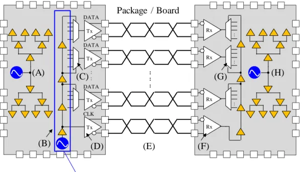
2.1 High-Speed Serial Link System
Fig. 2.1 shows an image of a high-speed serial link system. In Fig. 2.1, Tx and Rx represent transmitter and receiver, respectively. These chips operate based on some fundamental clocks. There are two different kinds of on-chip clock distribution systems.
One is a global clock distribution which is used for system clocking as shown in Fig. 2.1 (A) and the other is high-speed I/O clock distribution which is used for high-speed serial links as shown in Fig. 2.1 (B). The parallel data are converted to serial data at Fig. 2.1 (C) due to the limited number of I/O pins and output in differential signaling mode by transmitter at Fig. 2.1 (D). This differential signals are transmitted through a package and board as shown in Fig. 2.1 (E) and receiver blocks amplify the received data from small swing to VDD swing at Fig. 2.1 (F). After that, these serial data are converted to parallel data at Fig. 2.1 (G) and finally sent to the system at Fig.2.1 (H). Thus, high-
6 speed I/O clock distribution shown in Fig. 2.1 (B) requires the highest frequency due to the parallel to serial conversion. In this dissertation, we will focus on this high-speed I/O clock distribution and oscillator design.
Fig. 2.1 High-speed serial link system
2.2 Inverter Chain
Fig. 2.2 shows inverter chain on-chip clock distribution system [1]. Although this system is very simple, there are several problems as follows. First, since power consumption is proportional to power supply VDD2, the large output swing (0~VDD) makes power consumption worse. Second, the high-speed operation is difficult due to the large swing. Third, the power efficiency is low since the current is wasted during logic high to low transition. Forth, jitter is large due to the increase number of repeaters at high-speed, long distance condition. Fifth, it is vulnerable to both common mode and power supply noise due to the single-ended structure. Thus, this inverter chain structure is not suitable for high-speed, long distance on-chip clock distribution.
: Tx
: Tx
Tx
Tx DATA
DATA
DATA
CLK :
: :
: : :
Rx :
Rx :
Rx :
Rx
Scope of this study: high-speed I/O clock distribution
(A)
(B)
(C)
(D)
Package / Board
(F) (E)
(G) (H)
7 Fig. 2.2 Inverter chain architecture
2.3 Small Swing
Fig. 2.3 shows a small swing signaling structure. This structure is typically realized by CML (Current Mode Logic) [1]. Since the circuit is organized by differential topology, good CMRR (Common Mode Rejection Ratio) and PSRR (Power Supply Rejection Ratio) can be obtained. In addition, the reduced swing makes high-frequency operation possible. However, the power consumption caused by the constant current is a major drawback. Thus, this structure is not suitable for long distance clock distribution.
Furthermore, the minimum swing is limited by the sensitivity of receivers. Therefore, it is important that the total power consumption for both repeaters and receivers must be taken into consideration.
Fig. 2.3 Small swing architecture
I/O I/O
I/O I/O
I/O I/O
I/O I/O
buffer
repeater repeater
repeater repeater
I/O I/O
I/O I/O
I/O I/O
I/O I/O
CML CML CML CML
𝐼
𝑅 𝑅
8 2.4 Transmission Line Signaling
Fig. 2.4 shows the on-chip clock distribution system using a transmission line [2], [3]. This system can be applied when the wavelength is not negligible against the length of on-chip clock distribution line. Due to the recent high-speed and long distance trend, this structure is becoming more important these days. The advantages of transmission line are much better jitter performance due to the absence of repeaters and possibility of low-power operation if appropriate characteristic impedance and termination are selected. However, a time-consuming electro-magnetic (EM) simulation is necessary to extract parasitic inductance. In addition, an on-chip transmission line design requires many parameter optimizations such as width, space, height and frequency etc. The design methodology becomes much more complicated than conventional RC-based design. Hence, a simple methodology of on-chip transmission line modeling and optimization are necessary.
Fig. 2.4 Transmission line architecture
2.5 LC Resonance
Fig. 2.5 shows the on-chip clock distribution system using a LC resonance [4], [5]. Thanks to the charge recycling, the driver just compensates the resistive loss caused by both the inductor and the wire of on-chip clock distribution line. Therefore, this structure can achieve very high power efficiency. However, since the resonant frequency fosc is determined by (2.1), the required inductance L becomes too small at high CL
scenario. Practically, an accurate small L is difficult to design due to the parasitic
I/O I/O I/O I/O I/O I/O I/O I/O
buffer
9 inductance. Therefore, some repeater stages are required at high-frequency, long distance situation so as not to have a high capacitance load. As a result, the existing LC resonance structures suffer from the power consumption and jitter due to the increase number of repeaters.
𝑓𝑜𝑠𝑐 = 1
2𝜋√𝐿𝐶𝐿 (2.1)
Fig. 2.5 LC resonance architecture
2.6 The Proposed Structure
Fig. 2.6 shows the proposed on-chip clock distribution architecture. The proposed architecture makes full use of both LC resonance and transmission line. The LC tank is shared between the oscillation tuning capacitor CD and the load capacitance CL of clock distribution line. The blue dotted line shows the image of current distribution.
The effective load capacitance is reduced owing to the LC resonance at CL side. Thanks to this reduced effective capacitance, we can take out repeaters on the clock distribution line. Hence, we can utilize transmission line signaling. Since the clock distribution line is directly driven by a LC oscillator, the waveform is just a simple sinusoidal wave.
Therefore, the design can be much easier and robust than conventional pulse-based due to the absence of higher harmonics.
I/O I/O
I/O
I/O I/O I/O I/O I/O
𝐶𝐿 𝐶𝐿
10 Fig. 2.6 The proposed bufferless architecture
To realize the proposed system, we will investigate on the following three key designs.
1. Inductor design
The performance of the LC oscillator is mainly determined by an inductor. A differential LC oscillator needs a differential inductor. Although, a conventional differential inductor has good symmetry, it is difficult to achieve high-frequency and low-coupling features. Fig. 2.7 shows the image why a differential inductor is difficult to achieve high-frequency operation. The phase relationship for two adjacent wire is almost in-phase for single inductor whereas differential inductor's one is out-of-phase.
Therefore, the parasitic capacitance for differential inductor is larger than single inductor.
This effect makes high-frequency operation for differential inductor difficult. Next, Fig.
2.8 shows the image why low-coupling feature is important. For instance, in RF systems, the magnetic fields generated from LC oscillator interfere with other blocks such as LNA (Low Noise Amplifier), PA (Power Amplifier) etc. and sometimes it causes undesired modulation. To avoid this scenario, typically each block is located far away to get good isolation at the cost of layout area. Thus, we will investigate on the following structure as shown in Fig. 2.9. The proposed inductor places two identical single inductors in stepping order. This feature makes the self-resonant-frequency same as single inductor. In addition, the 8-shaped current distribution tries to cancel magnetic flux each other. However, we may lose the symmetry to a certain extent due to the
I/O I/O I/O I/O I/O I/O I/O I/O
LC oscillator
𝐶 𝐶 𝐶𝐿 𝐶𝐿
Current Loop
11 connectivity to form the 8-shaped current distribution. The goal of this study is to investigate if the proposed inductor can achieve the high-frequency, low-coupling and good symmetry as we expected.
Fig. 2.7 Research objective of fSR (self-resonant-frequency)
Fig. 2.8 Research objective of magnetic coupling
Fig. 2.9 Research objective of symmetry for 8-shaped differential inductor
single differential
high-fSR low-fSR
Oscillator LNA
Flipped order
Symmetry: perfect
Stepping order
Symmetry: relatively good
12 2. On-chip transmission line modeling and optimization
The proposed bufferless architecture utilizes the transmission line signaling mode. However, major problem of transmission line design is the design complexity.
The following procedures are necessary to perform one transmission line simulation.
Step-1. layout operation. Step-2. s-parameter extraction by EM (Electro-Magnetic)- simulation. Step-3. transient simulation by SPICE. There are several problems in this design procedure. First, since there are many parameters such as width, space and thickness etc. for transmission line design, the layout operations are time-consuming work if the parameter optimizations are necessary. Second, EM-simulation is usually expensive and takes time if the simulation area is large. Third, sometimes we have convolution errors in transient analysis from s-parameter to time-domain change and this is strongly dependent on SPICE simulator. Thus, we will investigate on the simple, accurate equivalent transmission line modeling and optimization without using EM- simulation as shown in Fig. 2.10. A 5-wire GSGSG physical structure is converted to an equivalent single-ended RLC-distributed model without using EM-simulation. The reason for the selection of GSGSG is to make the model accurate by adding GND to signal lines not only bottom but also side. Once a general 5-wire GSGSG structure is modeled, the same methodology can be easily applicable to other structures such as GSSG, SGS, SS. The single-ended model makes a basic transmission theory adoption possible. In addition, although conventional works only treat thick top metal layer, we will expand available metal layers to multiple layers. This is because top thick metal layer is commonly used for power supply mesh and it is not guaranteed that we can always utilize thick top metal layer for on-chip clock distribution line to avoid complexity of layout. Therefore, it is valuable to investigate what will happen if we utilize other metal layers such as metal-5, metal-4 etc. As for optimization, we will develop the algorithm to optimize delay, power consumption of driver and output swing from the given target specifications using the proposed equivalent model. The importance of delay and power are to satisfy the allowable timing budget and power of driver circuitry. The output swing is essential factor for level shift stages after clock distribution. Thus, the goal of this study is to develop the fully calculation-based design methodology of on-chip transmission line modeling and optimization.
13 Fig. 2.10 Research objectives of on-chip transmission line modeling and optimization
3. LC oscillator design
The proposed bufferless architecture shares LC-tank between frequency tuning capacitor CD and load capacitance CL as shown in Fig. 2.6. However, this new architecture has not been researched by any papers yet. For instance, oscillation frequency of a conventional LC oscillator is determined by only one resonant loop which is determined by (2.1). On the other hand, the proposed one has at least two resonant loops. Also, ideal inductor’s tap location is not clear. Thus, the goal of this study is to investigate on the basic theory of this new LC oscillator such as oscillation frequency, output swing and tap location etc. as shown in Fig. 2.11.
M6 only EM-simulation
All layer Fully-calculation
- RLC-distributed model
=
=
=
- Optimization
(delay, power, output swing)
G S G S G
G S G S G
G S G S G
M1 (Thin) M2 (Thin) M3 (Thin) M4 (Thin) M5 (Thin) M6 (Thick)
14 Fig. 2.11 Research objectives of LC oscillator
2.7 Chapter Summary
In this chapter, we briefly introduced the pros and cons of existing on-chip clock distribution systems. The conventional repeater-based on-chip clock distribution systems are not suitable for high-frequency and long distance systems due to the increase of power consumption and jitter caused by multiple repeater stages. The transmission line approach can reduce the number of repeaters. However, the design methodologies become complicated. It raised the necessity of a simple methodology of on-chip transmission line modeling and optimization. The LC resonance can improve the power efficiency owing to the charge recycling mode. However, repeater stages are still required due to isolate the capacitive load from LC oscillator. It raised the necessity of low frequency sensitivity LC oscillators. Based on the backgrounds of existing systems, we also briefly introduced the basic idea of our proposed system which makes full use of both transmission line and LC resonance mode.
𝐶 𝐿 𝐶𝐿
𝑉
𝐶 𝐿 𝐶𝐿
𝐿 𝐿 𝑉
Conventional Proposed
only one resonant loop
Which tap location is the best?
Two resonant loops.
How resonant frequencies
are determined? How big is output swing?
15 References
[1] K. Hu, et al., "Comparison of on-die global clock distribution methods for parallel serial links," IEEE International Symposium on Circuits and Systems (ISCAS), 2009.
[2] K. Banerjee and A. Mehrotra, "Analysis of on-chip inductance effects for distributed RLC interconnects," IEEE Transactions on Computer-Aided Design of Integrated Circuits and Systems, vol. 21, pp. 904-915, 2002.
[3] P. Heydari, S. Abbaspour, and M. Pedram, "A comprehensive study of energy dissipation in lossy transmission lines driven by CMOS inverters," Proceedings of the IEEE 2002 Custom Integrated Circuits Conference, 2002.
[4] J. Poulton, et al., "A 14-mW 6.25-Gb/s transceiver in 90-nm CMOS," IEEE Journal of Solid-State Circuits, vol. 42, pp. 2745-2757, 2007.
[5] K. Fukuda, et al., "A 12.3-mW 12.5-Gb/s complete transceiver in 65-nm CMOS process," IEEE Journal of Solid-State Circuits, vol. 45, pp. 2838-2849, 2010.
16
Chapter 3 Design of High-Frequency, Low-Coupling Inductor
Design of High-Frequency, Low-Coupling Inductor
3.1 Introduction
3.1.1 Background
In recent high-speed digital and RF systems, on-chip inductor plays an important role. For instance, a differential LC oscillator as shown in Fig. 3.1 is used in high-speed serial links to achieve both high-frequency and low-jitter requirements [1]. A conventional differential LC oscillator uses a differential inductor for the symmetrical outputs. However, the low self-resonant-frequency (fSR) has been a major drawback due to the long routing of wire [2]. In RF transceiver systems, strong magnetic fields from power amplifier (PA) interfere with local oscillator (LO). This mechanism results in injection locking [3]. Hence, each inductor must be located far away to a certain extent at a cost of large chip area. Thus, a differential inductor that has symmetry, high-fSR and low-coupling has been desirable.
Fig. 3.1 Differential LC oscillator
17 3.1.2 Previous Work
According to Findley et al. [2], a high-fSR differential inductor is introduced.
Although this inductor is high-fSR, low-coupling and symmetry features have not been achieved. On the other hand, some low-coupling and symmetry twisted inductors are introduced in papers [3] [4] [5]. However, high-fSR feature has not been achieved due to the long routing. Thus, there are no ideal differential inductors that can achieve symmetry, high-fSR and low-coupling features.
3.1.3 Objectives and Scope of This Study
The goal of this study is to develop the differential inductor which has high-fSR, symmetry and low-coupling features for LC oscillator. In this chapter, we will propose a novel high-frequency, low-coupling 8-shaped differential inductor with Patterned Ground Shield (PGS) [6]. The PGS structure can maximize the Quality factor while improving the Electro-Magnetic (EM) simulation time owing to the reduced number of nodes [7] [8]. The 8-shaped structure makes the symmetry, low-coupling and high-fSR
possible. The test chip is implemented in TSMC 0.18-μm 1-poly 6-metal CMOS process.
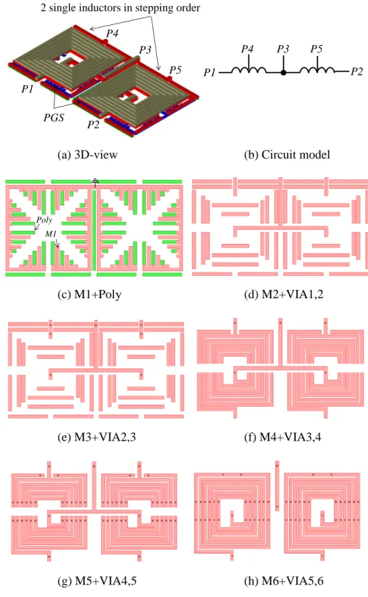
3.2 Inductor Design
The basic design of the proposed inductor is based on a single-inductor design.
For substrate shielding, we adopted PGS for improvement of Quality factor, accuracy of EM-simulation and reduction of the number of elements. For metal structure, Metal 6, 5, 4 are shorted together to reduce DC resistance while keeping the required fSR. We placed vias at metal edge only to mitigate the skin effect [9]. The proposed inductor is organized by placing two single inductors in stepping order as shown in Fig. 3.2. In Fig.
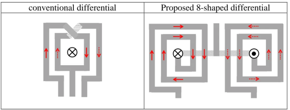
3.2, P1-P2, P3 and P4-P5 represent differential-input, center-tap and quarter-tap, respectively. Fig. 3.3 shows the comparison of the current distribution and magnetic fields between a conventional and the proposed differential inductor. The magnetic field of each inductor induced by the 8-shaped current distribution tries to cancel out far-field magnetic coupling each other. Hence, the proposed structure is able to achieve the symmetry, high-fSR and low-coupling features.
18
(a) 3D-view (b) Circuit model
(c) M1+Poly (d) M2+VIA1,2
(e) M3+VIA2,3 (f) M4+VIA3,4
(g) M5+VIA4,5 (h) M6+VIA5,6
Fig. 3.2 The proposed 8-shaped differential inductor
The green-, pink-color lines and dots are poly, metal and via from (c) to (h) P1
P2
P3 P4
P5 2 single inductors in stepping order
PGS
P1 P2
P3
P4 P5
Poly M1
19 conventional differential Proposed 8-shaped differential
Fig. 3.3 Current distributions and magnetic fields
3.3 Simulation Results
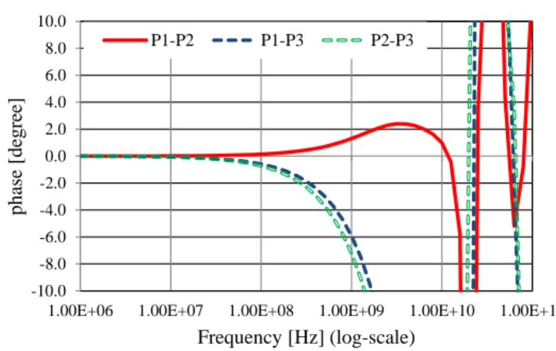
Table 3.1 shows the detailed design parameters of the proposed inductor. We used Keysight “Momentum-RF” for EM-simulation tool and performed s-parameter analysis at Fig. 3.4 condition. The differential L and Q are derived from s-parameter to z-parameter conversion using (3.1) to (3.3). Fig. 3.5 shows the comparison results between single (Fig. 3.4 (a)) and proposed inductor (Fig. 3.4 (b)). The proposed inductor achieved almost twice higher L while having a same fSR and Q compared with a single inductor. Fig. 3.6 shows the phase difference at Fig. 3.4 (c) configuration to check the symmetry of the proposed inductor. The phase difference is only 2.4 degree at 3-GHz and it is symmetrical enough for differential LC oscillator use. Fig. 3.7 shows the comparison results of L, Q at Fig. 3.4 (b) and (d) configurations. For Fig. 3.4 (d), the tap location has been chosen such that L at Fig. 3.4 (d) can be half of Fig. 3.4 (b) by using approximate equations introduced in the study of Mohan et al [10]. The simulation results showed good match with our expectations. Hence, the proposed differential inductor can be accurately and simply designed based on a single inductor design.
20 Table 3.1 Design parameters of our proposed inductor
Process TSMC 0.18-μm 1-poly, 6-metal
Metal structure M6(thick) // M5 // M4
Metal width 4.5-μm
Metal space 1.5-μm
N. of turns 6
Shielding PGS (Metal1 + poly)
Area 130 x 235 μm2
L at 3-GHz 6.22-nH (differential)
Q at 3-GHz 5.9
fSR 13.3-GHz
“//” represents short by vias.
(a) P1 – P3 (single) (b) P1 – P2
(c) P1 – P3, P2 – P3 (d) P4 – P5 Fig. 3.4 Measurement configurations
𝑍𝑑𝑖𝑓𝑓 = 𝑍 − 𝑍 − 𝑍 + Z (3.1)
𝐿 =𝑖𝑚𝑎𝑔(𝑍𝑑𝑖𝑓𝑓)
(2𝜋𝑓) (3.2)
𝑄 =𝑖𝑚𝑎𝑔(𝑍𝑑𝑖𝑓𝑓)
𝑟𝑒𝑎𝑙(𝑍𝑑𝑖𝑓𝑓) (3.3)
Here,
𝑍𝑑𝑖𝑓𝑓 : differential impedance 𝑓 : frequency 𝑖𝑚𝑎𝑔 : imaginary part 𝑟𝑒𝑎𝑙 : real part
P3
P4 P5
P1 P2 P1 P2
P3
P4 P5
P1 P2
P3
P4 P5
P1 P2
P4 P3 P5
21 (a) Inductance
(b) Quality factor
Fig. 3.5 Comparison between Fig. 3.4 (a) and Fig. 3.4 (b)
Fig. 3.6 Phase difference at Fig. 3.4 (c) configuration
0.00 2.00 4.00 6.00 8.00 10.00 12.00 14.00 16.00
1.00E+06 1.00E+07 1.00E+08 1.00E+09 1.00E+10 1.00E+11
Inductance [nH]
Frequency [Hz] (log-scale) L (Proposed-differential) L (single)
0.00 1.00 2.00 3.00 4.00 5.00 6.00 7.00 8.00
1.00E+06 1.00E+07 1.00E+08 1.00E+09 1.00E+10 1.00E+11
Quality Factor
Frequency [Hz] (log-scale) Q (Proposed-differential) Q (Single)
-10.0 -8.0 -6.0 -4.0 -2.0 0.0 2.0 4.0 6.0 8.0 10.0
1.00E+06 1.00E+07 1.00E+08 1.00E+09 1.00E+10 1.00E+11
phase [degree]
Frequency [Hz] (log-scale)
P1-P2 P1-P3 P2-P3
22 (a) Inductance
(b) Quality factor
Fig. 3.7 L, Q results at Fig. 3.4 (b) and Fig. 3.4 (d) configurations
0.00 2.00 4.00 6.00 8.00 10.00 12.00 14.00 16.00
1.00E+06 1.00E+07 1.00E+08 1.00E+09 1.00E+10 1.00E+11
Inductance [nH]
Frequency [Hz] (log-scale) L (P1-P2) L (P4-P5)
5.5nH
2.9nH
0.00 1.00 2.00 3.00 4.00 5.00 6.00 7.00 8.00
1.00E+06 1.00E+07 1.00E+08 1.00E+09 1.00E+10 1.00E+11
Quality Factor
Frequency [Hz] (log-scale) Q (P1-P2) Q (P4-P5)
23 3.4 Measurement Results
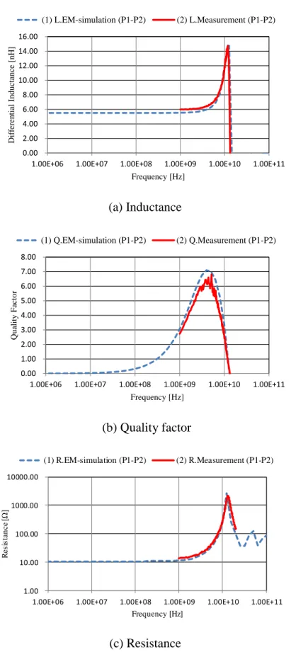
3.4.1 Inductance, Quality Factor and Resistance
Fig. 3.8 shows the photograph of the fabricated proposed 8-shaped differential inductor and measurement configurations. The proposed inductor is measured using 50Ω probe station and Keysight 8722C network analyzer. Fig. 3.9 shows the comparison results of L, Q, R between measurement and EM simulation. The measurement results showed good match with EM-simulation results.
Fig. 3.8 Photograph of the proposed 8-shaped differential inductor and measurement configurations
235um
130um
G S G S G
GSGSG probe
Keysight 8722C Network Analyzer
SMA cable
24 (a) Inductance
(b) Quality factor
(c) Resistance
Fig. 3.9 Measurement and EM-simulation results
0.00 2.00 4.00 6.00 8.00 10.00 12.00 14.00 16.00
1.00E+06 1.00E+07 1.00E+08 1.00E+09 1.00E+10 1.00E+11
Differential Inductance [nH]
Frequency [Hz]
(1) L.EM-simulation (P1-P2) (2) L.Measurement (P1-P2)
0.00 1.00 2.00 3.00 4.00 5.00 6.00 7.00 8.00
1.00E+06 1.00E+07 1.00E+08 1.00E+09 1.00E+10 1.00E+11
Quality Factor
Frequency [Hz]
(1) Q.EM-simulation (P1-P2) (2) Q.Measurement (P1-P2)
1.00 10.00 100.00 1000.00 10000.00
1.00E+06 1.00E+07 1.00E+08 1.00E+09 1.00E+10 1.00E+11
Resistance [Ω]
Frequency [Hz]
(1) R.EM-simulation (P1-P2) (2) R.Measurement (P1-P2)
25 3.4.2 Coupling Coefficient
Fig. 3.10 shows the photograph of fabricated four pair of 8-shaped differential inductor and measurement configurations. Each inductor is isolated by 20.5-μm spacing.
S-parameter is measured using Keysight E5071 4-port network analyzer. The coupling coefficient of mutual inductance (K) can be obtained by transformer basics as shown in Fig. 3.11. In Fig. 3.11, the voltage of port-1 and port-2 are defined as (3.4) and (3.5). In this configuration, if port-1 is input and port-2 is open, then i2 = 0 and v1, v2 can be expressed as (3.6), (3.7) respectively. Since v2 and i1 are known values, we can get mutual inductance M from (3.7). We can use the same manner in the case of port-1 is open, port-2 is input. Therefore, the coupling coefficient K can be defined as (3.8). Table 3.2 shows the number of combinations of K in this measurement setup. In Table 3.2, suffix of K represents labels of inductor. For instance, K12 represents K between IND-1 and IND-2. For EM-simulation, we used Integrand Software Inc. EMX. Fig. 3.12 shows comparison results of K between measurement and Electro-Magnetic (EM) simulation.
From Fig. 3.12 (a), the maximum K is as low as 0.03 and measurement result showed good match with EM-simulation at Δx=20.5μm. Fig. 3.12 (b) shows the Δx dependency which is interpolated by EM-simulation. This result shows that far-field magnetic coupling is canceled out as we expected and Δx=60μm is sufficient enough for better isolation. However, there is an error at Δx=261.5μm. We believe this error is caused by accuracy of EM-simulation.
𝑣1= 𝐿1∙𝑑𝑖1
𝑑𝑡 + 𝑀 ∙𝑑𝑖2
𝑑𝑡 (3.4)
𝑣 = 𝐿 ∙𝑑𝑖
𝑑𝑡 + 𝑀 ∙𝑑𝑖
𝑑𝑡 (3.5)
𝑣1= 𝐿1∙𝑑𝑖1
𝑑𝑡 (3.6)
𝑣2= 𝑀 ∙𝑑𝑖1
𝑑𝑡 (3.7)
𝐾 = 𝑀
√𝐿 ∙ 𝐿 (3.8)
26 Fig. 3.10 Photograph of the four pair of 8-shaped differential inductor and measurement
configurations
Fig. 3.11 Mutual inductance of transformer
Table 3.2 Combinations of aggressor and victim in four pair of inductor Parameters Aggressor Victim
𝐾 IND-1 IND-2
𝐾 3 IND-1 IND-3
𝐾 4 IND-1 IND-4
𝐾 3 IND-2 IND-3
𝐾 4 IND-2 IND-4
𝐾34 IND-3 IND-4
GSGSG probe
GSGSG probe
Keysight E5071C Network Analyzer
𝑣 𝐿 +
−
𝐿
+
− 𝑣
𝑖 𝑀 𝑖
27 (a) Comparison of K between EM-simulation and measurement results
(b) Dependency of distance for K
Fig. 3.12 Comparison of K between EM-simulation and measurement results -100.0
-90.0 -80.0 -70.0 -60.0 -50.0 -40.0 -30.0 -20.0
K12 K13 K14 K23 K24 K34
Couplingcoefficientk [dB]
Combination of coupling k (EM-simulation)
k (Evaluation) Δx=20.5μm
Δx=261.5μm
-100.0 -90.0 -80.0 -70.0 -60.0 -50.0 -40.0 -30.0 -20.0
0 60 120 180 240 300
Couplingcoefficientk [dB]
Distance of inductors Δx [μm]
k (Momentum-RF) k (Evaluation)
IND1-IND2 Δx=20.5μm
IND3-IND4 Δx=261.5μm
28 3.5 Chapter Summary
In this chapter, we proposed a high-fSR, symmetrical and low-coupling 8-shaped differential inductor with PGS for differential LC oscillators. The 8-shaped structure organized by two single inductors in stepping order realizes a high-fSR same as single inductors and the symmetry same as differential inductors. Hence, the proposed inductor makes full use of both single and differential inductor’s features. In addition, the proposed inductor can mitigate the far-field magnetic coupling owing to the 8-shaped current distribution. This feature not only improves the interference problems such as injection locking but also contributes to area-saving owing to the compact spacing. A PGS structure can maximize the Q-factor while improving the computational time and accuracy of EM-simulation due to the reduced elements. The measurement results showed good agreement with EM simulation.
29 References
[1] Poulton J, Palmer R, Fuller AM, et al., "A 14-mW 6.25-Gb/s transceiver in 90-nm CMOS.," IEEE Solid-State Circuits Society., vol. 42, pp. 2745-2757, 2007.
[2] Findley P, Ali Rezvani G, Tao J., "Novel differential inductor design for high self- resonance frequency.," IEDM Technical Digest. IEEE International Electron Devices Meeting, 2004.
[3] Nobuyuki Itoh; Hideaki Masuoka; Shin-ichi Fukase; Kenichi Hirashiki; Minoru Nagata, "Twisted Inductor VCO for Suppressing On-chip Interferences," Asia- Pacific Microwave Conference, 2007.
[4] Nathan M. Neihart; David J. Allstot; Matt Miller; Pat Rakers, "Twisted inductors for low coupling mixed-signal and RF applications," IEEE Custom Integrated Circuits Conference, 2008.
[5] Andrew Poon; Andrew Chang; Hirad Samavati; S. Simon Wong, "Reduction of Inductive Crosstalk Using Quadrupole Inductors," IEEE Journal of Solid-State Circuits, vol. 44, pp. 1756-1764, 2009.
[6] Masahiro Ichihashi; Haruichi Kanaya, "A high-frequency, low-coupling 8-shaped differential inductor with patterned ground shield," Microwave and Optical Technology Letters, vol. 60, pp. 2704-2707, 2018.
[7] Wong Y, "On-chip Spiral Inductors With Patterned Ground Shields For Si-based RF IC’s," Symposium 1997 on VLSI Circuits, 1997.
[8] Yim S, Chen T, K.K. O., "The effects of a ground shield on the characteristics and performance of spiral inductors," IEEE Journal of Solid-State Circuits, vol. 37, pp. 237-244, 2002.
30 [9] Xiangming X, Li P, Cai M, Han B., "Design of Novel High-Q-factor multipath stacked on-Chip spiral inductors," IEEE Trans Electron Devices, vol. 59, pp.
2011-2018, 2012.
[10] Mohan SS, del Mar Hershenson M, Boyd SP, Lee TH., "Simple accurate expressions for planar spiral inductances," IEEE Journal of Solid-State Circuits, vol. 34, pp. 1419-1424, 1999.
31
Chapter 4
On-chip Transmission Line Modeling and OptimizationOn-chip Transmission Line Modeling and Optimization
With the increases of frequency and chip area in recent digital VLSI systems, the design methodologies for on-chip clock distribution lines have been changing from an RC-model to an RLC-model. Hence, they must be treated as transmission lines. However, an on-chip transmission line design needs time-consuming Electro-Magnetic (EM) simulation which is not suitable for recursive optimizations such as metal width, space, length, thickness and the number of layers etc. within the practical time range. Therefore, a new design methodology without using EM-simulation is necessary. In this chapter, we introduce a fully calculation-based on-chip transmission line modeling and optimization methodology. The proposed methodology has been verified using a 9-mm on-chip clock distribution line at 3-GHz in the TSMC 0.18-μm 1-poly 6-metal CMOS process. The proposed fully calculation-based model showed good agreement with both EM-simulation and experimental results. We also show that the proposed optimization methodology can find the smallest physical structure while achieving the lowest power consumption from the given target specifications such as delay and output swing.
32 4.1 Introduction
4.1.1 Background
An on-chip clock distribution system is becoming one of the most power-hungry block in recent digital VLSI systems such as microprocessors, memories. For instance, a huge amount of power (from 25% to 70% in the chip) can be dissipated in the case of microprocessors [1], [2], [3]. As the frequencies and chip area increase, the effects of parasitic inductance have been prominent for the following reasons. First, a high signal slew rate makes the reactive impedance (jωL) higher than the resistive impedance (R).
Second, the reflection effects must be taken into consideration due to the relationship between the wavelength (λ) and the length of the clock distribution line as shown in Fig.
4.1. Hence, on-chip clock distribution design must be treated as a transmission line.
Fig. 4.1 Border line between RC and RLC-model
However, an on-chip transmission line design has many practical difficulties as follows. (1) Time consuming EM-simulation is required for parasitic inductance extraction. EM-simulation extracts the s-parameter based on the given physical structure.
Therefore, every time we try to run EM-simulation in different conditions, we must prepare different layouts. This recursive process is not suitable for optimization process despite recent improvements in computer processing. In addition, EM-simulators are
1 10 100
0.1 1.0 10.0
Length of Clock Line [mm]
Frequency [GHz]
line of λ/20
RLC Region
RC Region
This work
33 usually expensive. (2) Some convergence problems from the extracted s-parameter to the time-domain exist in the convolution process for SPICE simulation. Since these problems are strongly dependent on the SPICE simulator, sometimes we misunderstand the results. (3) There are many parameters such as width, space, length, the number of layers and combinations for optimization. For these reasons, an accurate, simplified RLC-model and optimization methodology have been desirable for circuit designers to estimate the best physical structure and parameters from the given target conditions without any EM-simulations.
4.1.2 Previous Work
Many works have been investigated on RLC-modeling and optimization. For RLC-models, some efficient and precise models have been reported [4] – [12]. However, most models use in part either EM or SPICE simulations. In addition, a research of interest is limited to a thick metal layer only even though multiple layers are available in the actual fabrication processes. Thus, there are currently no fully calculation-based RLC-models for multiple layers. For optimization methodologies, most of existing researches optimizes the delay and power consumption only although actual designs also need the large output swing [13] – [18]. The reason for the importance of large output swing is because receivers on the clock distribution line dissipate huge amounts of power to amplify the received signal from small swing to VDD at level shift stages. Thus, no optimization methodologies exist to handle the delay, power and output swing at the same time.
34 4.1.3 Objectives and Scope of This Study
The goals of this research is to develop the following two features: (1) to derive an accurate and simplified RLC-model for multiple interconnect layers (6 metal layers for this process) without any EM-simulations; (2) to derive an optimization methodology that can handle following three parameters at the same time using the proposed RLC- model. Namely, delay, power and output swing.
The conditions for this research are as follows. A differential signaling with a five-wire GSGSG configuration in a 9-mm straight line, as shown in Fig. 4.2 is used as a clock distribution structure. This structure is commonly used in high-speed serial links which require the highest frequency in the chip due to the parallel to serial conversion.
The length of 9-mm covers existing large chips and allows us to consider the transmission line effects. For the fabrication process, TSMC 0.18-μm 1-poly 6-metal CMOS is used due to limited available options in our laboratory. For the target frequency, we chose around 3-GHz because the estimated maximum frequency in the worst condition at Fan Out (FO) = 4 is around 3~4 GHz under this 0.18-μm process.
Although both frequency and process are not the most up to date, they can easily be applicable to different specifications since this research is about RLC-modeling and optimization methodology. In addition, the relationship between this target frequency and length is within the RLC region, as shown in Fig. 4.1. Therefore, we can discuss transmission line effects. Table 4.1 summarizes the design parameters.
Fig. 4.2 High-speed I/O clock distribution without repeaters
𝑇𝑅 𝑇𝑅 𝑇𝑅 𝑇𝑅 𝑇𝑅 𝑇𝑅
𝑅𝐿𝐶
![Fig. 2.3 shows a small swing signaling structure. This structure is typically realized by CML (Current Mode Logic) [1]](https://thumb-ap.123doks.com/thumbv2/123deta/9808097.1884982/21.918.172.816.102.286/shows-signaling-structure-structure-typically-realized-current-logic.webp)
![Fig. 2.4 shows the on-chip clock distribution system using a transmission line [2], [3]](https://thumb-ap.123doks.com/thumbv2/123deta/9808097.1884982/22.918.172.816.559.759/fig-shows-chip-clock-distribution-using-transmission-line.webp)