INVITED PAPER
Special Section on Analog Circuits and Related SoC Integration TechnologiesBackground Calibration Techniques for Low-Power and
High-Speed Data Conversion
Atsushi IWATA†a), Fellow, Yoshitaka MURASAKA†, Member, Tomoaki MAEDA†,
and Takafumi OHMOTO†, Nonmembers
SUMMARY Progress of roles and schemes of calibration techniques in data converters are reviewed. Correction techniques of matching error and nonlinearity in analog circuits have been developed by digital assist using high-density and low-power digital circuits. The roles of the calibration are not only to improve accuracy but also to reduce power dissipation and chip area. Among various calibration schemes, the background calibration has significant advantages to achieve robustness to fast ambient change. Firstly the nonlinearity calibrations for pipeline ADCs are reviewed. They have required new solutions for redundancy of the circuits, an error esti-mation algorithm and reference signals. Currently utilizing the calibration techniques, the performance of 100 Msps and 12 bit has been achieved with 10 mW power dissipation. Secondly the background calibrations of match-ing error in flash ADC and DAC with error feedback to the analog circuits are described. The flash ADC utilizes the comparator offset correction with successive approximation algorithm. The DAC adopts a self current match-ing scheme with an analog memory. Measured dissipation power of the ADC is 0.38 mW at 300 MHz clock. Effects of the background calibration to suppress crosstalk noise are also discussed.
key words: digital assist analog circuit, flash ADC, comparator, current summing DAC, substrate noise
1. Introduction
In analog-digital mixed CMOS LSIs, circuit architectures and design techniques of highly functional and accurate cir-cuits with low power dissipation and a small chip area are strongly demanded. The demands are based on contribution to the advancement of portable information systems, com-puting and sensor systems for healthcare and environment monitor.
Because the Vth deviation and the noise power of an MOS device and the accuracy of RC components are in-versely proportional to the square root of the area of the de-vices, it is not possible to scale the size of analog devices. Therefore, it is difficult to decrease the area of the chip and the power consumption of analog circuits. These drawbacks are contrast to the advantage in high density integration and dissipation power saving in digital circuits. The advantage is provided along with the congress of nano-meter device, low voltage circuit and fabrication process technologies.
In this paper, roles and schemes of the background cal-ibration techniques in analog circuits are reviewed. Nonlin-earity correction techniques for pipeline ADC by the digital-assisted techniques are described. Matching error
calibra-Manuscript received March 15, 2011.
†The authors are with A-R-Tec Corp., Higashihiroshima-shi,
739-0046 Japan.
a) E-mail: [email protected]
DOI: 10.1587/transele.E94.C.923
tion for ADC and DAC for high speed delta–sigma ADC is described. Accuracy improvement and dissipation power savings with digital calibration, in 4 bit flash ADC and 4 bit current summing DAC, are discussed. Furthermore, effects of background calibration against crosstalk noise are evalu-ated by the test chip measurement.
2. Roles of Calibration Techniques
In order to develop signal processing LSIs for audio, video, and wireless communication with low-power scaled CMOS devices, various A-D and D-A converters were proposed [1]. Continuing trend of device scaling has achieved low-power and high-density logic circuits. However accuracy, density and power dissipation of analog circuits have not received significant benefit. Design tradeoff in analog circuits and calibration effects are shown in Fig. 1.
Accuracy of analog circuits is limited by device noise, device matching error, nonlinearity and circuit noise. The most fundamental is the thermal noise of devices, which can be reduced only by cooling or statistical processing. The de-sign solution for reducing the 1/f noise of which the power is inversely proportional to the square root of gate area, is to enlarge device size while sacrificing current and a chip area. To reduce matching error of pair devices and weighting ele-ments, we have also to enlarge the device size. Nonlinearity caused by MOS characteristics and stray components, dose not directly depend on the device size. Since the matching error and nonlinearity are not fundamental, they can be re-solved by the calibration.
Fig. 1 Design tradeoff and calibration effects.
For many years, many kinds of calibration techniques are studied to improve circuit precision and SNR. The cal-ibration technique includes (i) trimming doing just after chip manufacturing, (ii) foreground calibration (FG Cal. for short) doing while system idling, and (iii) background cali-bration (BG Cal. for short) doing continuously during oper-ating. The trimming techniques with resistance adjustment using fuse or laser can correct only deviations in a wafer fabrication process. The FG Cal. which is applicable to the system with a stand by mode, can correct deviations of cir-cuits due to gradual changes in supply voltage, temperature and due to aging. In the BG Cal., since error correction parameters are continuously updated during operation, the deviation caused by fast change of environments can be sup-pressed.
In the first phase, the object of calibration is to enhance analog circuit accuracy without costly trimming for many elements. For that purpose, additional DACs and memories for the error correction are used. In the second phase, the ob-ject became to obtain high accuracy using low-accuracy ana-log circuits in corporation with a digital processing for cor-recting analog circuit errors. The technique is called “dig-ital assist” [2] and becomes indispensable in recent scaled mixed signal VLSIs. The role of the digital assist is consis-tent with enhancing accuracy of circuits, and saving a chip area and power dissipation. Though circuit deviations are large, analog circuits using the minimum sized MOS devices work at high speed with low power.
Recently by the progress of device scaling, redundant configurations have become applicable to commercial VL-SIs. Therefore the BG Cal. becomes important to realize dependable VLSI against extremely low supply voltage and severe environmental changes. By combined use of analog feedback correction, since calibration cycle of 100 ns can be achieved, the deviation by the fast change of ambient con-ditions can also be corrected. Moreover, the crosstalk noise form logic circuits and the environmental noise can be also corrected.
3. Calibration in Pipeline A-D Converter
3.1 Configuration of the Pipeline ADC
In the pipeline ADC, a cascade connection of converter stages, each of which consists of a multiplying DAC (MDAC for short) and sub-ADC with a redundant bit, has been widely adopted. In the commonly used 1.5b pipeline stage, the sub-ADC uses two comparators and the MDAC uses a 1.5b DAC and an amplifier as shown in Figs. 2(a) and (b). In the MDAC, the input signal Vinis amplified by a gain of two and the DAC output is subtracted from the amplified input signal to produce the output signal Voutcalled residue. Output digital data of all converter stages are processed in digital domain with correcting the errors. In this architecture which uses low resolution converter stages, nonlinearity of the residue amplifier is a major source of error, and the off-set error of the comparator is easily corrected. Since the
Fig. 2 Blockdiagram of pipeline ADC.
pipeline ADC is suitable for digital calibration, many kinds of techniques have been proposed [3]–[6].
3.2 Power Reduction of Residue Amplifiers
In order to reduce power dissipation of the ADC, the archi-tecture utilizing an open loop single stage residue amplifier and digital calibration of nonlinearity of the amplifier has been proposed [5]. To implement the BG Cal., superimpos-ing the modulation signal onto the input signal, nonlinear-ity is estimated during normal operation by the statistical algorithm and corrected by digital processing for the esti-mated inverse characteristics as shown in Fig. 2(c) [4]. In this scheme, a reduction of 60% of the power dissipation has been reported.
Settling time of the residue amplifier is a limiting factor to enhance the sampling rate. An incomplete settling error calibration approach has been proposed in which the gain er-ror is corrected by the digital calibration [6]. Effective gain in the incomplete settling varies significantly with ambient conditions of temperature and supply voltage. The effective gain variation is continuously corrected by the BG Cal. Uti-lizing this architecture, the power dissipation of the residue amplifier can be reduced to 10% and 40% of those using a high-gain closed loop amplifier and open loop single stage amplifier, respectively, with complete settling [5].
A more-advanced architecture using an analog feed-back calibration in addition to the digital feed-forward cali-bration has been proposed. For example a feedback loop that controls the amplifier operating bias point at the maximum gain spot has been proposed. Utilizing these mixed
cali-bration technologies, a 16 bit 250 Msps pipeline ADC was reported [6].
4. Calibration for Flash A-D Converters
Feature of the flash ADC based on the parallel compar-ison principle is high-speed conversion in low-resolution (<8 bit). It has been widely applied to the system for high frequency measurement, communication and control. The issues of the ADC are reduction of dissipated power and chip area required for a large number of comparators [7]. Accuracy of the converter is mainly determined by the de-cision level offset of each comparator caused by a device matching error. Because the offset deviation is inversely proportional to the square root of the gate area, the ordinary design approach enlarges the gate area. However, the large size devices consume large power to work at high speed. 4.1 Low Power Comparator with Small MOS Devices To achieve a high-speed and low-power conversion, a new approach utilizes minimum sized MOS devices. However accuracy of circuits such as the decision level of a compara-tor degrades unacceptably. The effective solution for the drawback is a calibration technique. To reduce the power dissipation of the ADC, the most suitable comparator is a differential dynamic latch comparator as shown in Fig. 3 [8]. A differential latch which consists of cross coupled clocked inverters is connected to the ground though four nMOS de-vices, whose gates are connected to the input voltages In+, In−, and the reference voltages Ref+, Ref−. While the clock Clk is “low”, output nodes N1 and N2 are “high”. When Clk goes to “high”, M1 and M2 turn on, and the output node voltages V1 and V2 are drawn to the ground level through input devices M1∼M4. For example, when the input volt-age Vin+ is high while Vin− is low, the drain current of M1 increases and that of M4 decreases. This results in a faster voltage change of V1 than that of V2. When Clk goes “high”, the comparator latches the decision result such that V1 is “low” and V2 is “high”. The decision result is deter-mined by the slew rate that depends on the drain currents of M1 and M4 and the capacitances of the nodes N1 and N2. Therefore the decision offset of the comparator can be cor-rected by adjusting the capacitance of nodes N1 and N2 [9].
Fig. 3 Dynamic comparator with offset calibration.
The capacitance is changed by the binary weighted C array with MOS gate capacitance, as shown in Fig. 3. Two C ar-rays are connected to the nodes N1 and N2. Depending on the polarity of offset, one side of the C array is used.
Required resolution of the C array is determined with a calibration range and resolution. The range is estimated by Monte Carlo simulation using matching error of input MOS devices. In this design, the calibration resolution of decision level is 3 mV (0.07LSB@4 bit) and the calibration range is 16LSB. Therefore the C array with 6 bit resolution is required.
4.2 Calibrated Comparator with SAR
Usually reference voltages of the ADC are generated using an R string, which consumes DC power. In stead of the R string, an architecture using the offset of each compara-tor generated by the mismatch of input MOS devices has been proposed [9]. Even though the power dissipation is reduced, we can not minimize the size of MOS devices be-cause weighting MOS devices are required.
A blockdiagram of the comparator cell with self cal-ibration circuits is shown in Fig. 4. During the calcal-ibration mode, inputs of the differential comparator In+ and In− are connected to differential reference voltages, Vr+ and Vr−. Each comparator cell has a circuit for acquiring the calibra-tion data automatically by the principle of the successive ap-proximation (SA) algorithm. The calibration data are stored on the registers and control the C array switches.
For background calibration, between 15 reference lev-els generated by the R string and 16 comparators, selectors are installed to connect each comparator cell to the corre-spondent reference level based on the calibration sequence. The SAR operates with the sampling clock. Since 10 clocks are required for one SAR operation and 16 comparators are calibrated one by one, the calibration period is 1.065µs at 150 MHz clock frequency.
4.3 Design Example and Performance
As an example of the BG Cal. of matching error, a 4 bit flash ADC was designed and fabricated with a 65 nm CMOS tech-nology. The layout of the ADC is shown in Fig. 5. Sixteen comparator cells which include the SAR for calibration are integrated. To suppress the kickback noise, reference levels
Fig. 5 Layout of the ADC.
Fig. 6 DNL of the ADC with calibration.
are generated by the R string with decoupling capacitors. The chip area is 150× 265 µm including the BG Cal. cir-cuits.
Measured power dissipation is 0.38 mW at 1.4 V sup-ply and 150 MHz clock frequency. The power consump-tion is reduced to about 1/10 by the effect of calibration and use of minimum size MOS devices. The ADC operates at the clock frequency of maximally 1 GHz. Measured DNLs with and without calibration are shown in Fig. 6. Though the DNL is 2LSBpp without calibration, it is improved to 0.2LSBpp by the BG Cal. and FG Cal., where the input range is 0.7 Vpp and 1LSB is 43.8 mV.
5. Calibration for D-to-A Converter
5.1 DAC Circuits and Calibration Methods
DAC architectures such as C array, R string and MOS ar-ray require a large number of weighting elements. In these schemes, high accuracy up to about 14 bit is obtained with-out calibration, but its chip area is drastically increased. They are not suitable to apply calibrations because they re-quire a large scale calibration circuits. On the other hand, R-2R ladder DAC and C-2C ladder DAC are implemented with a small number of elements and have relatively high sensitivity to the elements. These are suitable to apply the calibration because they require only small calibration cir-cuits.
Fig. 7 Basic current source with calibration.
Calibration methods of DAC include (i) resister trim-ming in R-2R DAC or R array DAC, (ii) adding calibration DAC operating with the correction data stored in a digital memory, (iii) calibrating each current source device of the current summing DAC by the gate voltage control with a capacitor as an analog memory.
5.2 Current Source for Background Calibration
The current summing DAC with unit current source cells is suitable to obtain high-linearity and high-speed settling. For low resolution (<6 bit) DAC, it is also suitable to apply calibration techniques. The linearity is determined by the matching error of each current source. Design strategy to use small size MOS current sources and to combine with the matching error calibration, achieves high-speed and low-power, and high-linearity by BG Cal.
The unit current source as shown in Fig. 7, is imple-mented with cascade connected MOS devices operated in saturation region [10]–[12]. In the calibration mode, SW1 is turned on and the output current is drained by the refer-ence current source. The referrefer-ence current source is com-monly used to all current sources. The output current of the current source is adjusted to match with the reference cur-rent by controlling the gate voltage of M2. The gate voltage is stored on a capacitor as an analog memory. To reduce the sensitivity to the gate voltage, current is divided to two passes through M1 for the constant bias and M2 is for the calibration. Ratio of the currents of M1 to M2 is 19:1. 5.3 Design Example and Performance
A circuit schematic of the 4 bit DAC with BG Cal. is shown in Fig. 8. One redundant current source is added for the BG Cal. While a D-A conversion operation, the current value of the selected current source by CAL1-CAL16 is calibrated one by one. Considering the settling time of the gate voltage of M2, 80 clock cycle/current source are required. 16 cur-rent sources are calibrated. The total calibration period is 4.26µs. A test chip of the DAC was designed and fabricated with a 65 nm CMOS process. A full scale output current range was design at 240µApp. The layout of the test chip is shown in Fig. 9. The chip integrates sixteen current sources
together with capacitors, logics for the BG Cal., and one reference current source. Though the number of devices in-creases, the device size of the current source is smaller than that of a no-calibration DAC.
Measured dissipation power of the test chip is 0.35 mW at 1.4 V supply, 300 MHz clock and 240µApp full scale out-put. Measured INL is shown in Fig. 10, comparing with no calibration and after BG Cal. INL is improved form 0.8LSB to 0.08LSB by the effect of calibration.
Fig. 8 Blockdiagram of the DAC with BG Cal.
Fig. 9 Layout of the DAC.
Fig. 10 Measured INL of the DAC.
6. Effect of Calibration against Ambient Noise
6.1 Effect of Background Calibration in the Flash ADC The crosstalk noise injected to a Si substrate and power sup-plies, degrades analog performances of mixed signal LSIs. The noise can be suppressed by the calibration. The effects were evaluated experimentally by the test chip which inte-grates on-chip noise sources and noise monitors [13]. Mea-surement conditions are as follows. The reference voltage is applied for 360 mV full-scale range. The input is trian-gle wave with 390 mVpp, and the sampling frequency is 150 MHz. From the output code, nonlinearity data were ac-quired by the histogram method. The INL characteristics with the noise injection are measured as shown in Fig. 11. The INL is as large as−0.5∼+1.5LSB without calibration. When the FG Cal. and BG Cal. are applied, the INLs are improved to−0.18∼0.17LSB, and −0.09∼0.15LSB, respec-tively.
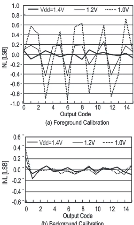
The effect of the calibration against the power-supply voltage change was evaluated in FG Cal. and BG Cal. Af-ter the FG Cal. is performed at Vdd=1.4 V, Vddis reduced to 1.2 V and 1.0 V. The measured INLs are shown in Fig. 12(a). The INLs are degraded to 0.6LSB and 1.5LSB at 1.2 V and 1.0 V, respectively. When the Cal. is performed con-tinuously, the degradation is within 0.1LSB, as shown in Fig. 12(b). This clearly shows a merit of the BG Cal. 6.2 Effect of Background Calibration in DAC
Changing the timing difference of the noise injection and the calibration clock, the INL with BG Cal. was measured, as shown in Fig. 13. In the timing difference from −10 ns to 0 ns, the INL is less than 0.2LSB even the noise is injected. After the timing t=0 ns, the INL increases and has a peak of 0.8LSB at t=50 ns. At this timing, because the calibrated Vg are stored on the capacitor, the noise causes an error of the stored voltage. Therefore the calibration complete timing should be moved before the clock edge of the noise source.
Fig. 12 Measured INL vs. supply voltage of the ADC.
Fig. 13 Measured INL vs. timing difference.
7. Conclusion
The roles and schemes of the calibration techniques for ADC and DAC have been reviewed focusing on the BG Cal. which provides robustness to ambient changes. The calibra-tion of nonlinearity of the pipeline ADC has been described. The calibration of matching error in the ADC and DAC has also been described based on the design of the 65 nm CMOS test chips and the measurements. The effects of BG Cal. to reduce crosstalk noise were also confirmed by the measure-ment.
Acknowledgments
This development was performed by the author for STARC as part of the Japanese Ministry of Economy, Trade and In-dustry sponsored “Silicon Implementation Support Program
for Next Generation Semiconductor Circuit Architectures”. The authors would like to thank Ms. Y. Harada, Mr. K. Chin, Mr. S. Fujikawa and Dr. Y. Masui with Hiroshima Univer-sity for chip design and measurement.
References
[1] B. Razavi, Principles of Data Conversion System Design, IEEE Press, Piscataway, NJ, 1995.
[2] B. Murmann, “Digitally assisted analog circuits,” IEEE Micro, vol.26, no.2, pp.38–47, March-April, 2006.
[3] U. Moon and B. Song, “Background digital calibration techniques for pipelined ADC’s,” IEEE Trans. Circuits Syst. II, vol.44, no.2, pp.102–109, 1997.
[4] B. Murmann and B. Boser, “A 12-bit 75-MS/s pipelined ADC us-ing open-loop residue amplification,” IEEE J. Solid-State Circuits, vol.38, no.12, pp.2040–2050, 2003.
[5] E. Iroaga and B. Murmann, “A 12-Bit 75-MS/s pipelined ADC us-ing incomplete settlus-ing,” IEEE J. Solid-State Circuits, vol.42, no.4, pp.748–756, 2007.
[6] A. Ali, A. Morgan, C. Dillon, G. Patterson, S. Puckett, M. Hensley, R. Stop, P. Bhoraskar, S. Bardsley, D. Lattimore, J. Bray, C. Speir, and R. Sneed, “A 16b 250 MS/s IF-Sampling Pipelined A/D Con-verter with Background Calibration,” Digest of ISSCC, pp.292–293, 2010.
[7] B. Razavi and B. Wooley, “Design techniques for speed, high-resolution comparator,” IEEE J. Solid-State Circuits, vol.12, no.12, pp.1916–1926, 1992.
[8] T.B. Cho and P.R. Gray, “A 10b 20 Msample/s 35 mW pipeline A/D converter,” IEEE J. Solid-State Circuits, vol.30, no.3, pp.166–172, 1995.
[9] G. Van der Plas, S. Decoutere, and S. Donnay, “A 0.16 pJ/ conversion-step 2.5 mW 1.25 GS/s 4b ADC in a 90 nm digital CMOS process,” ISSCC Dig. Tech. Papers, pp.566–567, 2006. [10] D.W.J. Groeneveld, H.J. Schouwenaars, H.A.H. Termeer, and
C.A.A. Bastiaansen, “A self-calibration technique for monolithic high-resolution D/A converters,” IEEE J. Solid-State Circuits, vol.24, no.6, pp.1517–1522, 1989.
[11] K. Falakshahi, C.-K.K. Yang, and B.A. Wooley, “A 14-bit 10-Msamples/s D/A converter using sigma-delta modulation,” IEEE J. Solid-State Circuits, vol.34, no., pp.607–615, 1999.
[12] S. Paton, T. Potscher, A. Di Giandomenico, K. Kolhau, L. Hernandez, A. Wiesbauer, M. Clara, and R. Frutos, “Linearity enhancement techniques in low OSR, high clock rate multi-bit continuous-time sigma-delta modulators,” Proc. CICC, pp.527–530, 2004.
[13] M. Nagata, J. Nagai, K. Hijikata, T. Morie, and A. Iwata, “Measure-ments and analyses of substrate noise waveform in mixed signal IC,” IEEE Trans. Comput.-Aided Des. Integr. Circuits Syst., vol.19, no.6, pp.671–678, 2000.
Atsushi Iwata received the B.E., M.S. and Ph.D. degrees in electronics engineering form Nagoya University, Nagoya, Japan, in 1968, 1970 and 1994 respectively. From 1970 to 1993, he was with the Electrical Communica-tions Laboratories, Nippon Telegraph and Tele-phone Corp. Since 1994, he was a professor of Electrical Engineering at Hiroshima University. Since 2009, he has been the CEO of A-R-Tec Corp. His research is in the field of circuit archi-tecture and design for ADC and DAC and low noise analog circuits. He received IEEE CAS Darling Award in 2007 and Outstanding Panelist Award at the 1990 ISSCC. Dr. Iawata is a member of the Institute of Electrical and Electronics Engineers.
Yoshitaka Murasaka received the B.E., and M.E. degrees in electrical engineering, form Hiroshima University, Japan, in 1999 and 2001, respectively. Since 2001, he was with A-R-Tec Corp. He is currently a research engineer of A-R-Tec Corp., Higashi-Hiroshima, Japan. His re-search area is focused on low-voltage analog cir-cuit design for low-noise systems.
Tomoaki Maeda received the B.E., and M.E. degrees in electrical engineering, form Hiroshima University, Japan, in 2001 and 2003, respectively. From 2003 to 2007, he was with the RF-semiconductor Development Cen-ter, Matsushita Electric Industrial Co., Ltd. Since 2007 he was with A-R-Tec Corp. He is currently a research engineer of A-R-Tec Corp. His research is focused on the area of low-voltage analog circuit design for low-noise sys-tems. Mr. Maeda is a member of the Institute of Electrical and Electronics Engineers.
Takafumi Ohmoto received the B.E., and M.E. degrees in physics, from Okayama and Hiroshima University, Japan, in 1992 and 1994, respectively. Since 2005, he was with A-R-Tec Corp. He is currently a research engineer of A-R-Tec Corp. His research is focused on the area of radiation and X-ray image sensors using SOI technology.