学位論文(要約)
Study on Epitaxial Perovskite Li-ion Conducting Thin Films:
Strain-controlled Ionic Conduction and Heterostructure
(
ペロブスカイト型Liイオン伝導体エピタキシャル薄膜の研究:
歪制御イオン伝導とヘテロ構造)
平成27年7月博士(理学)申請
東京大学大学院理学系研究科
化学専攻
韋 嵥
Study on Epitaxial Perovskite Li-ion Conducting Thin Films:
Strain-controlled Ionic Conduction and Heterostructure
by
Jie Wei
Department of Chemistry
Graduate School of Science
The University of Tokyo
Abstract
Li-ion conductors acted as solid electrolyte have attracted great attentions in the researches of all solid state Li-ion batteries. Among the known Li-ion conductors, lithi-um lanthanlithi-um titanate Li3xLa2/3−xTiO3 (LLT, 0.05 < x < 0.167) with A-site vacant perovskite structure shows the ionic conductivity up to 1 mS/cm at room temperature, which is comparable to those in conventional organic solvent electrolytes. Since grain boundaries significantly suppress the Li ionic conductivity in bulk LLT specimens, single crystal sample is required, but difficult to obtain in bulk study. The demand for obtaining single crystal has stimulated epitaxial thin film study to fabricate highly crystalline LLT. Recently, epitaxial thin film growth of LLT by pulsed laser deposition (PLD) attracted many interests to prepare single crystal specimens. However, in these researches, sto-ichiometric LLT was hard to obtained due to the Li-loss in fabrication process, thus it strangles further property investigation.
In this dissertation, highly crystalline epitaxial LLT thin film with stoichiometric composition was fabricated on various perovskite substrates. Laser fluence was discov-ered as the key factor related to the Li-loss and was varied to control Li-composition precisely. Also, Li-rich LLT target was used in PLD process in order to compensate the Li-loss observed in the previous experiments. By optimizing the laser fluence in addition to other PLD parameters, highly crystalline LLT thin film with stoichiometric composi-tion was obtained, enabling the measurement of intrinsically high ionic conductivity. The ionic conductivity in epitaxial thin films was comparable to that in polycrystalline specimens without showing grain-boundary conductivity which suppressed the total ion-ic conductivity in polycrystalline bulk study.
Strain-controlled effects on LLT crystal structure were investigated on LLT epitaxial thin films. By altering the substrates with different in-plane lattice constants, orientation
of LLT thin films was controlled as a-axis oriented with two kinds of in-plane domains perpendicular to each other under tensile strain, while c-axis oriented thin films were obtained with single domain under compressive strain.
Strain-controlled ionic conductivity of LLT was also investigated in LLT thin film on orthorhombic NdGaO3(110) substrate due to the anisotropic distortion of in-plane LLT lattice. In LLT epitaxial thin films, the ionic conductivity decreased with a increasing ac-tivation energy under an increasing compressive strain. The more contracted bottleneck generated from larger compressive strain enhanced the difficulty of Li-ion hopping. D-ifferent from the similar tendency showing in bulk research, the strain-controlled effects in epitaxial thin films are stable in the atmospheric condition. This research proved that epitaxial strain is very effective in controlling Li ionic conduction.
In addition, LLT heteroepitaxial structures were formed on La0.6Sr0.4MnO3(LSMO) bottom electrode layer as a preliminary study toward all solid state epitaxial Li-ion batter-ies. The interface between LLT and LSMO was studied in detail by X-ray reflectometry. LLT/LSMO interface was found to be rough as well as the interface between LLT and LSAT/SrTiO3substrates, probably due to Sr-La intermixing.
In conclusion, highly crystalline epitaxial LLT thin films with stoichiometric com-position were successfully fabricated. The researches on LLT thin films indicated that it is possible to control the crystal structure and ionic conductivity by applying epitax-ial strain. The investigations on heterostructure, which was formed by LLT thin film on LSMO bottom electrode, indicated the complicated interface structures and revealed the possibility to construct epitaxial battery structure by thin film growth. The strain-controllable LLT thin film as well as its heterostructure provides a deeper prospect to understand the intrinsic properties of LLT, leading to the application of all solid epitaxial device.
Acknowledgement
I want to give my great thanks to my supervisor Prof. Tetsuya Hasegawa, for all the academic guidance and encouragement. He provided me the opportunity to study in the University of Tokyo and the wonderful experimental environments. He has encouraged, supported and inspired me to investigate the infinite possibilities. Whenever I met the difficulties and hesitations, he was always more generous than sharing the knowledge.
I am very appreciated to work with Prof. Tomoteru Fukumura. His deep insight on solid state chemistry as well as patience and enthusiasm supported me through every research experience. He always encouraged me to challenge new ideas and fields without fearing about failure. With his supports, I acquired many academic skills as well as the thinking mode to bring out new ideas.
I would also give my thanks to Prof. Yasushi Hirose for his thoughtful advices in my experiments as well as the support in experimental techniques. I also owe this dissertation to Dr. Akira Chikamatsu, Dr. Hideyuki Kamisaka and Mr. Shoichiro Nakao for their kindness in sharing their experience to promote my research.
I would like to appreciate Dr. Daisuke Ogawa for his technical help in electrode fabrication and ionic conductivity measurement, in addition to his important contribution on this dissertation work. I would like to appreciate Prof. Atsushi Fujimori as the vice-supervisor in ALPS program for his fruitful discussion from the point view of a physicist. I am deeply grateful to Shungo Kojima, Shun Inoue, Thantip S. Krasienapibal, Ryosuke Sei, Mayuko Oka, Ken'ichi Kaminaga, Kyouhei Yamatake, Yutaka Uchida, Dai Kutsuzawa, Shunsuke Shibata as the members of the same project in daily discussion and supports in experiments. I also thanks to all the members in Hasegawa laboratory: Dr. Sohei Okazaki, Dr. Chang Yang, Dr. Youngok Park, Dr. Anri Watanabe, Tsukasa Katayama, Atsuchi Suzuki, Il Jeon, Xi Shen, Kazuki Aizawa, Kenta Shimamoto, Tomoya
Onozuka, Ryosuke Takagi, Kaori Kurita, Jumpei Takahashi, Masahito Sano, Vitchaphol Motaneeyachart, Takanori Yamazaki, Keisuke Kawahara, Yuji Kurauchi, Fahd S. Khan, Ryota Kantake, Keisuke Yamada, Naoki Kashiwa, Miho Otaki. I would also thank the secretaries, Ms. Mie Umino, Ms. Miki Komazawa, Ms. Mayumi Kikuchi and Ms. Aya Imoji for their supports.
I would give special thanks to Japanese government for providing MEXT scholar-ship as financial support in the past five years. I also thanks ALPS program and JFE Mineral for the opportunity of internship.
Finally, I would like to express my gratefulness to my family for their devotion and supports all the time.
Contents
1 General introduction 1
1.1 Lithium-ion battery . . . 1
1.2 Liquid electrolytes . . . 3
1.3 Inorganic solid electrolytes . . . 5
1.4 Lithium lanthanum titanates . . . 7
1.4.1 Bulk study . . . 7
1.4.2 Thin film study . . . 13
1.5 Purpose of this study . . . 16
2 Experimental methods 17 2.1 Sample preparation . . . 17
2.1.1 Pulsed laser deposition . . . 17
2.2 Crystallography analysis . . . 20
2.2.1 X-ray Diffraction . . . 20
2.2.2 Reflection high-energy electron diffraction . . . 24
2.3 Structure analysis . . . 26
2.3.1 Atomic force microscopy . . . 26
2.3.2 X-ray Reflectometry . . . 27
2.4 Composition analysis . . . 28
2.4.1 X-ray photoelectron spectroscopy . . . 28
2.4.2 Inductively coupled plasma optical emission spectroscopy . . . 29
2.4.3 Atomic absorption spectroscopy . . . 30
2.5 Ionic conductivity analysis . . . 32
2.5.2 Electrochemical impedance spectroscopy . . . 33
3 Thin film growth of Li0.33La0.56TiO3and strain-controlled ionic conductivity 38 3.1 Introduction . . . 38
3.2 Experimental methods . . . 38
3.3 Results and discussions . . . 39
3.3.1 Laser fluence dependence of Li-composition . . . 39
3.3.2 Laser fluence dependence of thin film growth rate . . . 44
3.3.3 Optimization of LLT thin film growth . . . 45
3.3.4 Structure analysis of LLT thin films . . . 48
3.3.5 Composition analysis of LLT thin films . . . 52
3.3.6 Ionic conductivity analysis of LLT thin films . . . 56
3.4 Summary and conclusion . . . 63
4 Heterostructure for Li0.33La0.56TiO3with conductive bottom electrode 65 4.1 Introduction . . . 65
4.2 Experimental methods . . . 66
4.3 Results and discussions . . . 67
4.3.1 Fabrication of LSMO buffer electrode . . . 67
4.3.2 Fabrication of LLT thin films on LSMO bottom electrodes . . . 69
4.3.3 Impedance spectra of LLT thin films in out-of-plane direction . 72 4.3.4 Interface study on heterostructure of LLT epitaxial thin film . . 74
4.4 Summary and conclusion . . . 77
5 General conclusion 79
1
General introduction
1.1
Lithium-ion battery
Rechargeable batteries, also known as secondary batteries, have become key com-ponents of modern electronic industry due to the explosively increasing needs of portable entertainment devices in mobile society. Among all kinds of rechargeable batteries, Li-ion battery (LIB) is one of the most popular type because of its high energy density, lack of memory effect and slow rate of charge loss when not in use. It is also more en-vironmental friendly and safer than its precursors such as lead acid batteries which are commonly used in traditional vehicles. Therefore, it has become a commercially avail-able candidate of replacement in electronic vehicles industry. However, compared with the spectacular advances in energy consuming technologies such as computers and mo-bile devices, technology of batteries still cannot keep the pace and is always criticized for its slow development. This requirement has driven a large number of researches in this field to develop batteries with higher energy density, faster charge rate and more charge cycles with less safety concern.
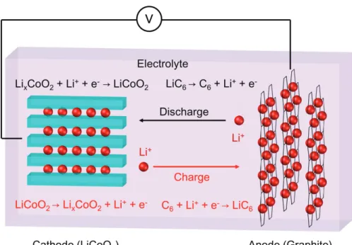
Figure 1.1 shows a representative structure of commercial LIBs. The commercial LIBs are generally based on Li-intercalated metal oxide cathodes and graphite anodes. When charging LIBs, Li+will deintercalate from the cathode and deposit on the anode side. On the other hand, when energy is extracted from LIBs during discharging, Li+ moves to the cathode side from the anode. Similar to traditional primary batteries, LIBs contain cathode, anode and electrolyte as their components. On the other hand, LIBs utilize Li-ions, not electrons as charge transfer species, making the unique requirement of material selections due to the high electropositivity and instability of Li compounds. By reviewing the history of LIBs technology, one can find the present status of research
and challenges for the future.
Figure 1.1 Schematic structure of commercial LIBs
Experiments based on lithium metal anodes began in the age of early 20th century, when G. N. Lewis proposed his theory about acid and alkali. The motivation to apply Li metal as anode was driven by the fact that Li is the lightest metal with high elec-tropositivity so that the theoretical energy density is rather high. However, it was hard to form a rechargeable cell due to lack of suitable cathode until Li intercalation into layered transition metal dichalcogenides was discovered in 1970s [1].
The first practical LIBs structure was proposed by M. S. Whittingham in 1976 at Exxon with a layered TiS2cathode and Li metal anode to achieve a cell voltage of 2.5 V,
although they suffered from safety issues due to the highly reactive anode [2, 3, 4]. In 1979, J. Goodenough demonstrated a rechargeable LIB using layered LiCoO2 as
cath-ode and Li metal ancath-ode to perform a cell voltage of 4 V [5], whose layered metal oxide cathodes became the most commonly used electrode in LIBs industry till now. In 1980, R. Yazami proposed the first prototype of graphite anode for LIBs through proving the
reversible intercalation of Li in graphite by electrochemical reaction [6]. In 1985, A. Yoshino, Asahi Kasei Co. claimed a patent about the prototype of LIBs, using metal oxides as cathode and carbonaceous materials as anode with a separator and nonaque-ous electrolytes [7]. In 1991, Sony and Asahi Kasei released the first commercial LIB product, representing the birth of LIB industry [8]. Since LIBs were born, most of the researches focused on the improvement of capacity and charge-discharge rate by devel-oping new cathode and anode materials. During the past two decades, the energy density of LIBs has increased by three times while the cost has dropped to 1/30 of the original product [9].
1.2
Liquid electrolytes
Compared with the significant advances in electrodes, improvement of electrolytes seems not notable. Until now, most of the commercial LIB products are still using the same type of electrolytes as twenty years ago, which are based on lithium salts and organ-ic alkyl carbonates solvents. A standard type of electrolyte is lithium hexafluorophos-phate (LiPF6) dissolved in ethylene carbonate (EC) mixed with ethyl methyl carbonate
(EMC), diethyl carbonate (DEC) or/and dimethyl carbonate (DMC) [10, 11]. These elec-trolytes have high ionic conductivity up to 10 mS/cm at room temperature, high anodic stability due to the wide potential range vs. Li/Li+ and low fabrication cost. However, disadvantages of these electrolyte solutions are also obvious for LIBs, which are [11, 12]:
• Low stability against temperature. The solutions freeze at low temperature and the ionic conductivity drops significantly, while at elevating temperature over 60◦C, the vapor pressure of the solvent increases drastically with explosion risk.
• Not compatible for shaped and light LIBs. As they are liquid, most of the LIB-s productLIB-s have to be covered by metal LIB-shellLIB-s to LIB-seal up the electrolyteLIB-s. ThiLIB-s
increases the weight of battery and is not flexible for varied shapes and sizes in mobile and micro devices.
• Decomposition of salts. It is believed that LiPF6can decompose into LiF and PF5
by a reversible process (Equation (1.1)). An unavoidable trace amount of water brought from fabrication process will easily react with the strong Lewis acid PF5
as represented by the following mechanism (Equation (1.2)) [13]. As a result, insolvable LiF deposits on surface of electrodes, blocking the Li diffusion path by passivation layers, while HF causes corrosion of cathode materials. Also, HF may react with ROLi and ROCO2Li species at the electrode surface, forming LiF and
reducing the total capacity in the battery.
LiPF6−−⇀↽−− LiF↓ + PF5 (1.1)
PF5+ H2O−−→ PF3O + 2 HF (1.2)
• Decomposition of solution. K. Kumai et al. proposed the following mechanism (E-quations (1.3) to (1.6)) for solution decomposition by analyzing the gas generated from LIBs using GC/MS [14]. It is believed that the generation of these flammable alkyl gases causes most of the explosion accidents. Because of the safety concern of explosion, logistics of LIBs requires licenses and high cost to prevent accidents in distribution network.
ROCO2R + Li++ e− −−→ ROCO2Li↓ + R · (1.3) ROCO2Li + Li++ e− −−→ Li2CO3↓ + R · (1.4)
R· + H2−−→ R−H + H · (1.5)
R· + R · −−→ R−R↑ (1.6)
In order to solve these problemes, stable solid state electrolytes are required. One of the commercialized approach is to solidify the liquid electrolytes by mixing with
poly-mers [15, 16]. However, inevitable dissolution of those solidified species is still a prac-tical problem.
1.3
Inorganic solid electrolytes
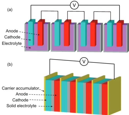
Inorganic solid lithium ion electrolytes are considered to take the place of organic solvents and polymer-based ones, due to their high thermal stability at a wide temperature range and inflammable property related to the safety concern. Moreover, LIBs using inorganic solid electrolytes can be more compact by using multiple stacking structure (Figure 1.2) [17], leading to higher practical energy density. Solid electrolytes are also flexible to shape and size, supporting the micro battery in micro devices in chip industry and medical applications. To realize the potential applications, inorganic solid electrolyte materials require various functional properties including [17, 18]:
Figure 1.2 Comparison of multiple stacking LIBs using (a) liquid electrolytes and (b)
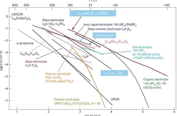
Figure 1.3 Ionic conductivity of various solid electrolytes, together with liquid
elec-trolytes solutions, polymer electrolyte and gel elecelec-trolytes. Reprinted by permission from Macmillan Publishers Ltd: Nature Materials [19], Copyright 2011.
• High total ionic conductivity up to 1 mS/cm.
• Chemical stability against reactions at electrode-electrolyte interface. • Low charge-transfer resistance at solid-state electrode-electrolyte interface. • Low cost fabrication method.
To achieve these goals, a large number of researches have been studied in the past few decades for discovering new materials. Various types of inorganic materials from amorphous to crystalline, from oxides to non-oxides, have been investigated, including lithium dopedβ-alumina (Li-β-Al2O3) [20], Li3N [21, 22], phosphates with sodium su-per ionic conductor structure (NASICON-type) [23], lithium susu-per ionic conductor type oxides (LISICON-type) [24], glass electrolyte (LiPON [25], Li2S-P2S5[26] and Li2 S-SiS2-Li3PO4[27]), Thio-LISICON Li3.25Ge0.25P0.25S4[28], perovskite Li3xLa2/3−xTiO3
(LLT) [29], garnet-type Li5La3M2O12 (M = Nb, Ta) [30], Li10GeP2S12(LGPS) [19] and so on. Among them, LLT, Li3N and LGPS exhibit high ionic conductivity as shown in Figure 1.3. Although LGPS shows the highest room temperature ionic conductivity up to 10 mS/cm which is comparable to LiPF6solution electrolytes, it suffers great drawback from the sulfide-oxide dead layer at the interface between cathode and electrolyte [31] as well as the instability against moisture and reduction [32]. Li3N, another material with high ionic conductivity up to 5 mS/cm, has a low decomposition potential vs Li/Li+(0.44 V) [22]. Therefore, its application to all-solid-state battery should be quite limited to low voltage cell.
1.4
Lithium lanthanum titanates
As mentioned above, perovskite type lithium lanthanum titanates Li3xLa2/3−xTiO3
(LLT, 0 < x < 0.16) has high ionic conductivity up to the order of 1 mS/cm under room temperature. Compared with other inorganic solid state electrolytes, it is stable over a wide range of temperature and is also available as a high voltage cathode due to its high electrochemical stability.
1.4.1 Bulk study
LLT was first fabricated by Y. Inaguma et al. in 1993 by solid state reaction through sintering a stoichiometric mixture of Li2CO3, La2O3 and TiO2[29]. LLT has an ABO3 perovskite structure as shown in Figure 1.4. The A-site in perovskite structure is not fully occupied by Li+and La3+, but contains a certain amount of vacancies, allowing hopping of a Li-ion to its neighbour A-site through a bottleneck formed by four O-ions.
Figure 1.4 Perovskite structure of LLT. Reprint with permissions from ''Epitaxial
Strain-Controlled Ionic Conductivity in Li-Ion Solid Electrolyte Li0.33La0.56TiO3Thin Films'',
Jie Wei, Daisuke Ogawa, Tomoteru Fukumura, Yasushi Hirose and Tetsuya Hasegawa,
Cryst. Growth Des., 2015, 15(5), 2187-2191. Copyright 2015 American Chemical
So-ciety.
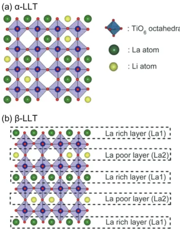
LLT has a mixture of two phases, high-temperature A-site disordered α-LLT and low-temperature A-site orderedβ-LLT, featured by the distribution of Li+ and La3+, as shown in Figure 1.5. Reversible phase transition was proved by Y. Harada et al. by controlled cooling process of bulk samples [33, 34]. They claimed that quenching re-sulted in A-site disordered cubic LLT, in which A-site cations were randomly arranged, while slow cooling process introduced A-site ordered tetragonal phase. T. Okumura et al. studied local structures of the two phases by extended X-ray absorption fine structure [35]. They believed that the A-site ordering changes the inter-atomic Columbic repul-sion force between lithium and surrounding ions, which generates the difference of ionic migration behavior between two kinds of LLT.
Figure 1.5 Structure of (a) A-site disorderedα-LLT and (b) A-site orderedβ-LLT. Re-produced from Ref. [35] with permission of The Royal Society of Chemistry.
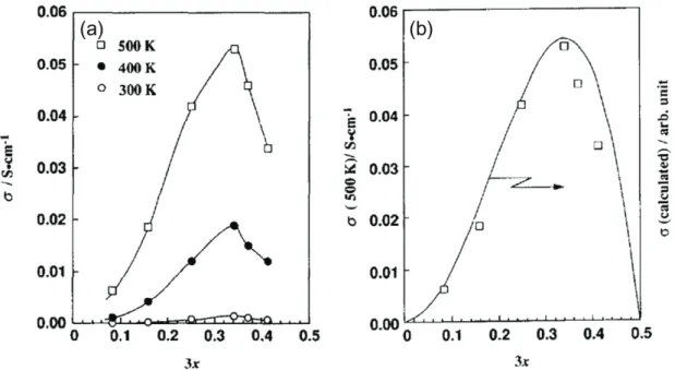
It is believed that the ionic conductivity of LLT is mainly governed by carrier con-centration and bottleneck size. As for the former, Y. Inaguma et al. studied the influence of carrier concentration by varying x in Li3xLa2/3−xTiO3and discovered that ionic
con-ductivity is a parabolic function of x with a maximum at x = 0.11 (Li0.33La0.56TiO3), as
shown in Figure 1.6 [36]. They proposed an empirical equation to describe this relation as Equation (1.7). σ ∝ m(1 − m)(n′− nc)2 = 3x(1/3− 2x) (1/3 + x)2 [ (1 3+ x)− nc ]2 (1.7) whereσ is the ionic conductivity, n′ is the total concentration of lithium and vacancy,
mis the ratio of lithium concentration to n′, ncis a constant equals to 0.3117 for simple
Figure 1.6 Ionic conductivity of LLT (a) as a function of x at various temperatures and
(b) comparison to calculation by Equation (1.7). Reprinted from Ref. [36], Copyright 1996, with permission from Elsevier.
Figure 1.7 High resolution transmission electron microscopy images for the (a) Li-poor
Li0.16La0.62TiO3and (b) Li-rich Li0.33La0.56TiO3polycrystalline bulk samples. (c)
Lat-tice parameter ratio across 90◦ domain boundaries along the direction of arrows shown in (a) and (b), respectively. Reproduced from Ref. [37] with permission of The Royal Society of Chemistry.
It is also known that the concentration of Li does not only affect the ionic conductiv-ity. Several neutron diffraction studies have indicated that the occupancies of La and Li in rich LLT [38] were different from those in poor LLT [39], resulting in varied Li-diffusion behavior [40]. X. Gao et al. studied the microstructures of Li-rich and Li-poor
LLT by scanning transmission electron microscopy [37, 41] and observed more distorted domain boundaries with angle of 90◦in Li-poor LLT samples (Figure 1.7), suppressing the migration mobility of Li-ions.
Figure 1.8 (a) Pressure dependence of bulk ionic conductivity in polycrystalline Li0.35La0.52TiO2.96. (b) Ionic conductivities (open circles) and activation energies (open
square) of Li0.34Ln0.56TiO3(Ln = La, Pr, Nd) in relation with their lattice parameters ap
at room temperature and atmospheric pressure. Solid circle and square show the ionic conductivity and activation energy of LLT under 1.0 GPa, respectively. Reprinted with permission from [42]. Copyright 1995, The Electrochemical Society.
As for the bottleneck, Y. Inaguma et al. studied the effect of compressive strain on ionic conductivity in LLT through hydrostatic pressure and replacement of La by Ln (Ln = Pr and Nd) with smaller ionic radius (Figure 1.8) [42]. By applying hydrostatic pressure up to 1.2 GPa, ionic conductivity of LLT dropped with an increasing activation energy. Similar tendency was observed by replacing La with Pr and Nd, where the LLT lattice shrank due to the smaller ionic radius of A-site cations. From their results, it was concluded that both mechanical and chemical compressive strains lead to low ionic con-ductivity and high activation energy in LLT. Furthermore, they calculated the activation volume for ionic conductivity and it was consistent with the activation volume derived
from the four-oxygen bottleneck hopping mechanism, indicating that bottleneck size was the key factor affecting the ionic conductivity. Since tensile strain was not easy to apply on bulk samples directly, T. Okumura et al. used F-doping on anion site to expand the bottleneck, resulting in improvement of ionic conductivity [43, 44].
Figure 1.9 Cole-Cole plots for LLT with Au electrodes measured at 300 K. Reprinted
from Ref. [29] Copyright 1993, with permission from Elsevier.
Although LLT has attracted great interest for its high bulk ionic conductivity, its disadvantage is also obvious: low grain boundary ionic conductivity. Figure 1.9 shows typical complex impedance Cole-Cole plots for polycrystalline sample [29]. One can find that the resistance of grain boundary in large semicircle contributed too much to the total ionic conductivity. Compared with the bulk ionic conductivity up to the order of 1 mS/cm, the grain boundary ionic conductivity is only of the order of 10−2 mS/cm, two orders lower than that of bulk. To solve this problem, single crystal LLT is required. Y. Inaguma et al. attempted to apply floating zone method to fabricate single crystal LLT
[45], but the obtained crystal contained domains with an average size of 100 nm [46]. Till now, there is still no other reports on bulk single crystal LLT, demonstrating the difficulty of single crystal fabrication.
1.4.2 Thin film study
Since fabrication of single crystal was difficult for bulk LLT samples, many re-searchers changed the strategy to synthesize single crystal LLT in thin film sample by epitaxial growth. Epitaxial growth, whose schematic processes shown in Figure 1.10, is very attractive to obtain single crystal thin film with particular orientation. It is a promising method for basic researches in physical properties and micro device applica-tions. Materials in the upper layer tend to have the same crystal structure and the same crystal orientation as the single crystal substrate, enabling us to construct high quality single crystal thin films with well-defined crystallographic orientations. This character-istic advantage allows easier observation for physical properties. Besides, the epitaxial stress from substrate can strongly affect the thin film layer and stabilize the tensile and compressive epitaxial strain in the thin film under atmospheric condition.
Figure 1.10 Schematic of epitaxial thin film growth.
Obtaining epitaxial LLT was still not easy and early thin film studies were almost based on polycrystalline, amorphous or composite samples. K. Kitaoka et al. first fab-ricated Li0.5La0.5TiO3 thin films by sol-gel method on non-alkali aluminoborosilicate
polycrystalline form with a preferred orientation of LLT(111) direction. O. Maqueda et al. deposited Li0.33La0.56TiO3thin films on polycrystallineα-Al2O3substrates by pulsed
laser deposition (PLD) [48] and obtained polycrystalline LLT with nanocrystalline struc-ture. Several amorphous LLT thin film studies were published in the past decade by PLD method [49, 50]. However, most of them suffered from low ionic conductivity in these polycrystalline or amorphous thin film.
Epitaxial thin film study was first reported by M. Morcrette et al [51] in 1998. They fabricated 001 oriented LLT thin film with LLT 110 impurities on MgO (001) substrate by PLD method. M. Morales et al. followed this work by using radio frequency magnetron sputtering method in 2002 and reported detailed information of LLT 001/110 epitaxial relationship on MgO (001) substrates [52]. However, both of them suffered from high Li-loss during fabrication of thin films, resulting in very low ionic conductivity.
Figure 1.11 La/Ti and Li/Ti ratio in targets and films fabricated at 750◦C and oxygen pressure of 100 mTorr on Pt (111) substrates. Reprinted from Ref. [53], Copyright 2013, with permission from Elsevier.
D. H. Kim et al. first systematically studied the Li-loss of LLT thin film during PLD process [53]. By carefully analyzing Li/Ti ratio and La/Ti ratio in targets with various compositions and thin films fabricated from these targets, they claimed that more than 50% Li-loss was observed between the targets and thin films while the La/Ti ratio was
almost kept, as shown in Figure 1.11. Based on this result, they fabricated LLT epitaxial thin film on SrTiO3 (100) substrate from a Li-rich Li0.64La0.49TiO3target and obtained
LLT thin film with 001 orientation and some impurities.
In 2012, T. Ohnish et al. fabricated LLT epitaxial thin films on SrTiO3 (100) and NdGaO3 (110) from a stoichiometric Li0.33La0.56TiO3 target by PLD method [54] and
got phase pure LLT with 100 and 001 orientations, respectively. The in-plane ionic con-ductivity of the film grown on NdGaO3 (110) substrate was 3.5× 10⁻⁵ S/cm with an activation energy of 0.35 eV, while measurement on SrTiO3 (100) failed for unknown reason. Although no boundary ionic conductivity was observed, such low ionic conduc-tivity was possibly due to Li-loss. Similar to this research, K. Mitsuishi et al. fabricated Li0.33La0.56TiO3 epitaxial thin film on Pt (111) substrate and analyzed the texture
Naz-ca line structure [55], but their report lacks of information about composition and ionic conductivity.
R. Kanno's group fabricated Li0.17La0.61TiO3epitaxial thin films on Al2O3(0001)
and Nb:SrTiO3 (111) substrates by PLD method and obtained phase pure LLT (111) thin films [56]. On Al2O3 (0001), they observed high in-plane ionic conductivity of 3.76× 10⁻⁴ S/cm at room temperature, close to bulk ionic conductivity of polycrys-talline bulk. They also fabricated a SrRuO3(111) / LiMn2O4(111) / LLT(111) epitaxial heterostructure as a half electrode of battery on Nb:SrTiO3(111) substrate, showing re-versible electrochemical reaction up to 4.5 V vs Li/Li+[57]. However, since LLT (111) direction is not the intrinsic Li diffusion path according to the bulk study, their films are not suitable for measuring the intrinsic property. In addition, out-of-plane ionic conduc-tivity was not mentioned in this report.
In summary, epitaxial LLT thin film is a good solution to avoid low boundary ionic conductivity, though fabrication is still difficult mainly due to Li-loss. In addition, it
is also expected that tensile strain will lead to expansion of four-oxygen bottleneck for Li-hopping, considering from the results of bulk researches. More efforts to investigate its intrinsic properties are required in this research field including material synthesis and applications to battery.
1.5
Purpose of this study
As mentioned above, there are still many issues in the research field of LLT thin film growth, including Li-loss during film fabrication and low ionic conductivity. Also, effects of strain applied from substrates on ionic conductivity was not fully understood. Meanwhile, epitaxial thin films are suitable for studying strain controlled ionic conduc-tivity which is not accessible in atmospheric condition in bulk samples. Moreover, the reason for failure in ionic conductivity measurements on SrTiO3substrates is unknown and no information was provided about the out-of-plane ionic conduction.
In this study, I focused on PLD fabrication of LLT epitaxial thin film along its intrin-sic axis in perovskite structure. I investigated the effect of PLD parameters on Li-loss to fabricate stoichiometric phase pure LLT thin film with high quality. Different substrates with varied lattice constants were used to apply different strains on LLT thin film. I also studied the effect of in-plane epitaxial strain on ionic conductivity and crystal struc-ture including lattice constant and orientations. LLT with conductive bottom electrode epitaxial heterostructure was fabricated to understand its out-of-plane ionic conductive behavior. In addition, interface between substrate, conductive electrode and LLT was characterized by X-ray reflection in order to investigate the multi-layer structures and the reason for failure of ionic conductivity measurements on SrTiO3substrates.
2
Experimental methods
2.1
Sample preparation
2.1.1 Pulsed laser deposition [58, 59]
Pulsed laser deposition (PLD) is a well-established technique for high-quality thin film fabrication. PLD is a specified physical vapor deposition technique using a high power laser beam to produce material source so that it allows deposition of materials with low vapor pressure. Since its invention in 1965 and success in fabricating high-temperature superconductor YBa2Cu3O7−δ epitaxial thin film in 1987, this technique
has become a common method for inorganic material thin film research.
Figure 2.1 Schematic figure of PLD system
Figure 2.1 shows a schematic figure of typical PLD system. The system is com-posed of an ultrahigh vacuum chamber maintained by rotary pump and turbo molecular
pump, an ultraviolet pulsed laser, substrate heating system and focused optical systems. A target, which is used as a material source, is set at an angle of 45◦ to the laser beam. Parallel to the target surface, there is a single crystal substrate set above.
Pulsed laser deposition is considered to include the following processes [58, 59]:
• Light absorption in solid. When the target is irradiated with an ultraviolet pulsed laser, target surface absorbs the high energy of photons and is decomposed into particles and clusters containing ionized and atomic species. For a homogenous target, the energy absorption is similar for all the components in the target. If the intensity of laser beam within the laser spot is uniform, all components can evaporate in a stoichiometric way.
• Plasma generation. By a very complicated process during continuous photon ex-citation by the pulsed laser within ns-scale, species are injected perpendicular to the target surface to form a plasma and gain high kinetic energy with high density and temperature. As the excited temperature is extremely high, all the species are ionized with similar efficiency.
• Transfer of plasma. The generated plasma expands toward the substrate set right above under Coulomb repulsion and recoil, generating a spatial distribution of plas-ma called ''plume''. The plume size and spatial distribution of each species strong-ly restrong-ly on the scattering within the dense plasma and with molecules intentionalstrong-ly introduced in the chamber. The scattering yield is related with element mass, ve-locity of species, density of plume and background pressure [60, 61]. This will cause expansion of plume and give non-uniformity within the plume depending on the expanding angle.
arriving atoms and ions will lose most of their kinetic energy and deposit as a thin film. Crystallization will also happen if enough energy for nucleation and surface migration is supplied by heating and interaction with substrate lattice. However, some of the species with low cohesive energy to substrate surface will be easily removed again from substrates due to collision of high energy species within the plasma, as called ''re-sputtering effect''. This will also cause non-stoichiometric transportation from target to substrates.
In early researches by PLD method, species are considered to be stoichiometrically transferred from target to substrate, without significant derivation of composition. How-ever, many recent studies proved that PLD process may cause noticeable composition change of Li [62, 63], including Li-loss in LLT thin film study [53]. Therefore, pre-cise control of parameters in PLD system is required to achieve the desired composition in thin film, including laser fluence, repetition rate, substrate temperature, background pressure and species, target composition and substrate.
In this work, I developed a PLD system equipped with a 248 nm KrF excimer (Co-herent CompexPro 50) laser for target ablation. Laser ablation fluence was varied by a half-wavelength attenuator plate with fixed laser output energy and beam size. High-purity oxygen gas was introduced through a variable leak valve to control the background pressure. LLT targets were synthesized by solid state reaction and sintered as ceramic pel-lets. Several kinds of perovskite oxide single crystals were chosen as substrates for LLT thin film growth. Substrates were fixed on an oxidized Inconel alloy plate by Inconel clamps. Backside of the oxidized Inconel plate was irradiated by an 808 nm infrared laser. Substrate temperature was controlled by the output power of the infrared laser and monitored by a pyrometer.
2.2
Crystallography analysis
2.2.1 X-ray Diffraction [64, 65]
X-ray diffraction (XRD) is one of the most common and non-destructive method to obtain crystallography information of solid materials. X-ray has a wavelength at 10−10 m level, so that the diffraction can precisely reflect the crystal lattice structure with the same order. Since the penetration depth of X-ray is usually larger than film thickness, not only thin film lattice, but also the epitaxial relationship between thin film and substrate can be characterized by thin film XRD technique.
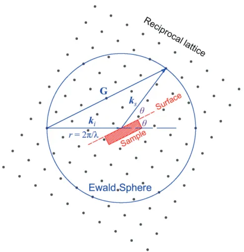
Principle of XRD can be described by reciprocal lattice and Laue's equation. Re-ciprocal lattice is the lattice of a crystal in its momentum space, or called k-space, whose spatial wavefunction is the Fourier transform of that in the original lattice. For a 3D lattice with infinite periods, the reciprocal lattice can be described as
b b b111= 2π aaa222× aaa333 aaa111· (aaa222× aaa333) b b b222= 2π aaa333× aaa111 aaa111· (aaa222× aaa333) b b b333= 2π aaa111× aaa222 aaa111· (aaa222× aaa333) (2.1)
where aaaiii is the primitive vectors in the original lattice, bbbiii is the primitive vectors in the
reciprocal lattice. The linear combination of these vectors forms reciprocal vector G,
G = hbbb111+ kbbb222+ lbbb333 (2.2)
where h, k and l are respective integers representing indices of a reflection plane. When X-ray is scattered by a lattice plane, the wavevectors of photons and lattice
vectors meet the Laue's equations: a aa111· (kkksss− kkkiii) = 2πh a aa222· (kkksss− kkkiii) = 2πk a aa333· (kkksss− kkkiii) = 2πl (2.3)
where kkkiii and kkksss are the incident and scattered wavevectors, with a norm of 2π/λ,
re-spectively.
Figure 2.2 Cross section of Ewald sphere in a reciprocal lattice of cubic structure
One can find that only when G = kkksss− kkkiii, Laue's equations satisfy. Since XRD
equipment has a fixed kkkiii, the information of reciprocal vector G is obtained by
measure-ment of scattered X-ray wavevector kkksss. In a perceptual intuition, one can draw a sphere
beam in the reciprocal space, called Ewald sphere (Figure 2.2). On the direction of kkksss
where diffraction is observed, there is a reciprocal lattice point at the intersection of kkksss
vector and Ewald sphere.
In a polycrystalline sample, crystals orient randomly, so that the diffractions on all the directions with the same cone vertex angle on Ewald sphere are equivalent, resulting in circular diffraction patterns. On the other hand, in a single crystal or oriented crystal such as epitaxial thin film, detailed information of crystal geometry results in a point-like diffraction pattern.
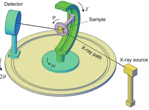
A typical 4-axis XRD equipment used for epitaxial thin film study is shown in Fig-ure 2.3. Samples can be tilted along the azimuth direction described by an angleω rela-tive to the X-ray incident beam. Samples can also be tilted along the two altitude direc-tions perpendicular to each other, described by anglesχ andϕ. The detector can move along another circular rail, in an angle 2θ to the X-ray incident beam. By controlling angles 2θ,ω, χ,ϕ, one can characterize crystal lattice by various mode, including
• 2θ-θ scan:ωis fixed at half of 2θ. In this mode, Laue's equations can be converted to Bragg's law:
2dsinθ = nλ (2.4)
where d is the distance between lattice planes perpendicular to the angle bisector of incident and scattered beams,λ is the wavelength of incident X-ray and n is an integer.
In epitaxial thin film analysis, one can specify the target lattice plane by tilting the angle χ andϕ. Lattice constants can be calculated from Equation (2.4) through geometric relationships. The data are usually shown as 2θ-θ plots with 2θ as horizontal axis and diffraction intensity as vertical one. This is one of the most common scan modes in XRD measurement.
• Rocking curve: ω scan with fixed 2θ,χ andϕ. The distribution of peak intensity can be obtained from this mode. Because real crystal does not have infinite lat-tice and is not perfect, and also X-ray generated from equipment is not perfectly coherent, XRD peaks will broaden and usually follow Gaussian distribution. The data are usually shown as rocking curves withω versus diffraction intensity. The full width at half maximum (FWHM) of rocking curves is used as a measure of crystallinity, viz quality of crystals.
• Pole figure andϕ-scan: ϕ scan with fixed 2θ, χ andω. The symmetry of peaks can be determined by this mode. Since symmetry is determined by crystal struc-ture, the same diffraction peak appears in equivalent directions. By rotating the sample along altitudeϕ direction, one can discover the number of equivalent di-rections and characterize the symmetry of crystal. In thin films, one can understand the epitaxial relationship between substrate and thin film through comparing the symmetry of each lattice. The data are usually shown as pole figure, which is the
stereographic projection of Ewald sphere from zenith pole, orϕ-scan plots withϕ versus diffraction intensity.
• Reciprocal space mapping (RSM): a cross section of reciprocal space. By perform-ing 2θ-ω scan at each ω, cross section of reciprocal space is obtained. The data are usually converted to a map with qqqxversus qqqz, where qqqx and qqqz are the inverse of lattice along in-plane and out-of-plane directions. Through RSM imaging, one can analyze the epitaxial relationship of crystal lattices between substrate and thin film.
In this study, XRD measurements were performed with a 4-axis diffractometer (Bruker AXS, D8 Discover). The equipment contains three kinds of detectors: 0D scin-tillation detector, 1D linear detector (VANTEC-1) and 2D detector (VANTEC-500) for different modes of measurements.
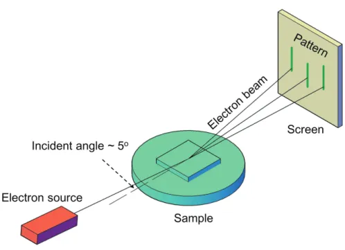
2.2.2 Reflection high-energy electron diffraction [66]
Reflection high-energy electron diffraction (RHEED) is also a technique using diffraction for characterization of lattice in solid materials. Different from XRD men-tioned above, RHEED utilizes high energy electrons as an incident beam and it is very sensitive to surface lattice.
Figure 2.4 shows a typical setting of RHEED system. An electron gun ejects elec-trons with high energy of 10-50 keV. The electron beam irradiates on the sample surface at a very small angle and is reflected toward a monitor screen. Because of the grazing angle, the penetration depth of electron beams is 1 nm level so that only the information of surface lattice is obtained. RHEED system can be installed in a designed PLD vac-uum chamber. Therefore in-situ monitoring of thin film growth is possible by RHEED measurement.
Figure 2.4 Schematic structure of RHEED
The principle of RHEED is similar to that of XRD. Since RHEED is surface sensi-tive, it is reasonable to apply 2D reciprocal lattice in this case. A 2D reciprocal lattice can be described as b b b111= 2π aaa222× nnn aaa111· (aaa222× nnn) b b b222= 2π nnn× aaa111 aaa111· (aaa222× nnn) (2.5)
where aaaiii is the primitive vectors in the original lattice, bbbiii is the primitive vectors in the
reciprocal lattice and nnnis the normal vector of lattice plane.
Since reciprocal lattice in 2D becomes rods perpendicular to the sample surface, typical RHEED image shows a rod like pattern for a flat surface. One can calculate the reflection angle 2θ from the geometry of equipment setting as well as the distance of rod patterns on the screen. Based on the obtained 2θ, the in-plane lattice constants can be calculated by using Bragg's law and lattice geometry. From the calculation result, information of in-plane lattice constant, in-plane symmetry, epitaxial relationship and surface reconstruction can be obtained.
Another important application of RHEED is in-situ observation of thin film growth process, especially layer-by-layer growth mode. In layer-by-layer growth, species will randomly distribute on the surface of thin film at first, and then form a perfect coverage before moving to the next layer. The intensity of RHEED during thin film growth will show a climax when one layer is formed and a minimal during random layer growth. This results in an oscillation in peak intensity and the period of oscillation represents the growth rate of thin film. In this study, RHEED system was installed on the PLD chamber for in-situ observation of thin film growth.
2.3
Structure analysis
2.3.1 Atomic force microscopy [67]
Atomic force microscopy (AFM) is a type of scanning probe microscopy with very high spatial resolution of the order of 1 nm. Using an AFM, it is possible to observe a sample surface at nanometer scale and analyze its roughness.
Figure 2.5 shows a schematic of AFM system. The system contains a cantilever with tips whose apex consists of several atoms, a laser generator, an array-type photon detector and a sample stage controlled by piezoelectric driver. AFM measures the force between atoms, including van der Waals force, static electric force, Casimir effect and etc. If only van der Waals force is considered, the force can be considered in a very simple model described by Lennard-Jones potential as
V = A ( 1 r )12 − B ( 1 r )6 (2.6)
where A and B are constants, r is the distance between a pair of neutral atoms.
Therefore, when the cantilever approaches the surface of sample, the atomic force changes with the distance between tip and surface atoms. This force induces bending of cantilever, resulting in a displacement of reflected beam by the back side of cantilever, which is measured by a photon detector. By probing sample surface through the dis-placement of reflected beam, the morphology of sample surface is observed. Because the tip apex is at atomic level, the spatial resolution can reach nanometer scale.
In this study, AFM measurements were performed by a commercial scanning probe microscopy system (SPI-4000, Hitach High Technologies).
2.3.2 X-ray Reflectometry [68]
X-ray reflectometry (XRR) is a technique to characterize the properties of thin films, including film thickness, surface roughness and density. It measures the intensity of reflected X-rays from a sample surface in relationship with incident angle.
XRR is a surface sensitive method. When the sample surface is perfectly flat, the reflection of X-rays will follow Fresnel conditions. The derivations from Fresnel condi-tion can be measured to estimate the film properties mencondi-tioned above approximately as
given by L. G. Parratt: R(Q) = RF(Q) ρ1∞∫−∞∞ eiQz ( dρe dz ) dz 2 (2.7)
where R(Q) is the reflectivity, RF(Q) is the Fresnel reflectivity representing a perfect
reflection, Q is the momentum transfer of X-ray described as Q = 4πsinθ/λ, θ is the incident angle,λ is the wavelength of X-ray, z is the depth of sample,ρ∞is the density at infinite depth of the material andρeis the average electron density profile in the sample.
Simulation of this equation yields the roughness of a sample surface and the density profile of a sample. For thin films grown on substrates and multilayers, XRR will show not only Fresnel reflectivity, but also oscillations. These oscillations can be explained by Fabry-Pérot effect: the X-rays reflected by the upper surface of thin film interference with the ones reflected by downer surface at characteristic incident angles related with thickness of thin films. Therefore, XRR is also used to analyze the thickness of thin film samples.
In this study, XRR was performed with the same instrument of XRD. Diffrac.Suite Leptos software package was used to simulate the depth profile of thin films measured by XRR.
2.4
Composition analysis
2.4.1 X-ray photoelectron spectroscopy [69]
X-ray photoelectron spectroscopy (XPS) is a technique to investigate electronic structures of materials and to measure elemental compositions quantitatively. Accord-ing to photoelectric effect discovered by Einstein, electrons will escape from material surface by providing enough energy with photon irradiation. This technique detects the kinetic energy of electrons emitted by X-ray photon irradiation to examine the binding
energy of each electron using the following equation:
Eb= hv− Ek−ϕ (2.8)
where Eb is the binding energy of electron, hv is the energy of X-ray photon, Ek is the
kinetic energy of emitted electron measured by the instrument, ϕ is the work function related to machine and material.
As X-ray energy is high, not only valence electrons of elements, but also inner elec-trons can be emitted by X-ray beam, showing specific peaks of elements for qualitative analysis. In addition, the intensity of XPS peaks representing the number of electrons is related with the amount of corresponding element. By integrating the peak intensity in XPS spectra, quantitative analysis of chemical composition is also possible. However, for light elements such as Li, XPS has low efficiency to propagate photoelectrons due to the low binding energy. For these elements, only semi-quantitative analysis is possible.
In this study, XPS measurements were performed by a commercial XPS system (PHI5000 VersaProbe, ULVAC-PHI). Li compositions in LLT targets and thin films were semi-quantitatively analyzed by XPS.
2.4.2 Inductively coupled plasma optical emission spectroscopy [70]
Inductively coupled plasma optical emission spectroscopy (ICP-OES) is a quanti-tative analytical method to detect metal elements in solution at trace level. ICP-OES is based on two parts, excitation/ionization of sample in the inductively coupled plasma (ICP) and quantitative measurement by optical emission spectroscopy.
In ICP process, the solution samples are loaded with Ar gas into a fused silica tube as aerosols. The tube is surrounded with a coil. By controlling the frequency and power in the coil, strong and high frequency electromagnetic field is generated, resulting in the
formation of electron discharge at the outlet of silica tube. The generated electrons col-lide with Ar atoms and lead avalanche phenomenon of electron discharge, thus plasma is created with extreme high temperature up to 10000 K. Sample aerosol is converted into an atomic vapor within the plasma and gain enough energy for ionization and pho-ton emission. Because the temperature of the plasma is sufficiently high, the ionization efficiency is usually more than 90% for metal species, enabling quantitative analysis for trace amounts.
After vaporization and ionization by ICP, the amount of each element are mea-sured by optical emission spectroscopy. Because the elements are heated in the high-temperature plasma, electrons in atoms are excited from a lower energy level to a higher one by heat. The excited electrons are not stable so that they will lose their energy by emitting photons and transit to lower energy states. As the energy states of atoms are discrete, the light emission results in discontinuous spectrum and can be measured by a spectrometer. The discontinuous spectrum is characteristic for each element according to the electronic structure. By observation of the designated wavelength and its intensity, qualitative and quantitative information of each element is obtained.
In this study, ICP-OES measurements were performed by a commercial ICP-OES instrument with external standard method for La and Ti composition analysis. ICP-OES was not suitable for Li analysis because an emission line of Ar gas partially overlapped with that of Li.
2.4.3 Atomic absorption spectroscopy [71]
Atomic absorption spectroscopy (AAS) is a technique based on the light absorption of atoms. Absorption is just the opposite process of emission. In absorption spectroscopy, samples are evaporated to provide atoms in the most stable ground state. Because the
energy levels are discrete in atoms, the electrons in the ground state can absorb light with a characteristic wavelength and be excited to a higher energy level. The degree of light absorption increases as the number of atoms increases. Therefore the quantitative analysis is possible.
Ideally, the light absorption in a homogenous sample can be described by Beer-Lambert law as
A = log10It I0
=ε· l · c (2.9)
where A is the absorbance of sample, I0and It are the luminous intensity of incident and
transmitted light,ε is the molar attenuation coefficient, l is the thickness of sample and
cis the concentration of measured species.
According to Beer-Lambert law, concentration is proportional to absorbance. How-ever, in most of the cases, the relationship between concentration and absorbance is not linear, because of various reasons including matrix effect of solution, low ionization ef-ficiency, non-homogenous evaporation, absorption by nearby lines and etc. Therefore, calibration by standard solutions is necessary.
In this study, a graphite furnace atomic absorption spectroscopy (GFAAS) instru-ment was used for Li composition analysis. Samples were transferred on a piece of graphite and heated to atomic vapors. A hollow-cathode lamp with wavelength of 670.78 nm was used as a light source. Quantitative analysis was carried out by external standard method.
2.5
Ionic conductivity analysis
2.5.1 Electrode preparation
In order to measure in-plane ionic conductivity, microelectrodes were patterned by photolithography and deposited by electron beam evaporation in an ultrahigh vacuum chamber. Photolithography is a technique to fabricate designed micro patterns on thin films or surface of bulk substrates.
A typical schematic of electrode preparation is shown in Figure 2.6.
Figure 2.6 Schematic process of electrode preparation by photolithography
The detail processes are:
• Cleaning: The sample is cleaned to remove surface contaminations.
• Photoresist preparation: A layer of photosensitive polymer, which is called ''pho-toresist'', is coated on the sample and dried by heating.
• Exposure: The prepared photoresist is covered with a photomask, which is made of a piece of glass coated with Cr metal patterns. After alignment of the photomask to specified position, UV light is irradiated through the transparent parts of pho-tomask and make the photoresist exposed.
• Developing: A part of photoresist is removed by a selected solvent, called ''devel-oper'', and rinsed in another solution to remove the photoresist thoroughly. Gener-ally, there are two kinds of photoresist, positive photoresist whose exposed parts are removed and negative photoresist whose non-exposed parts are removed.
• Ashing: Sample surface is cleaned with ozone plasma to remove contaminations from the developing process.
• Electrode deposition: The cleaned sample is transferred into an ultrahigh vacuum chamber. Electrodes are deposited by electron beam evaporation method.
• Remove photoresist: After the electrode deposition, the remained photoresist is re-moved by a specified solvent called ''remover'' as well as the metal covered above.
In this study, microelectrodes were prepared on thin film samples by using a positive photoresist and deposited with Ti/Au metals. All these processes were performed in a clean room to avoid dust contamination.
2.5.2 Electrochemical impedance spectroscopy [72]
Electrochemical impedance spectroscopy (EIS) is a technique to measure the current and voltage as well as the phase angle in relation with frequency of an alternating current (AC) circuit. EIS is usually used to analyze ionic conductivity, dielectric property, and electrode-electrolyte interface in electrochemical reactions.
The impedance, which is the opposition to a current when applying a voltage, is defined as the complex ratio of the voltages to the currents, with a symbol Z in usual. The data of impedance spectroscopy are usually plotted as Cole-Cole plots (or Nyquist plots) with the real part of impedance versus the imaginary one, and Bode plots with two curves composed of the impedance versus frequency curve and the phase angle versus
frequency curve.
In a circuit where electrons take the role of charge transfer, the impedance values of resistor, capacitor, inductor, series connection and parallel connection are described as Table 2.1, where ω is the angular frequency given by ω = 2πf, f is the frequency of AC circuit, R is the resistance, C is the capacitance, L is the inductance and Ziis the
component of series or parallel circuits. These device elements are very important in analysis of electronic devices, especially dielectric constants of materials.
Table 2.1 Impedance values of elements in a circuit
Element Current vs Voltage Impedance
Resistor V = IR Z = R Capacitor CdV dt = I Z = 1 iωC Inductor V = LdI dt Z = iωL Series Z =∑n1Zi Parallel 1 Z = n
∑
1 1 ZiOn the other hand, in electrochemical reactions and ionic conductive materials, the charge transfer is conducted by ions, which also cause mass transfer. The diffusion of mass becomes important in this case and diffusion elements have to be considered in the impedance spectrum. The diffusion of mass can be considered as linear diffusion following Fick's law. For a semi-infinite linear diffusion, it can be described as
∂c
∂t = D
∂2c
where c is the concentration of ions, x is the coordination for diffusion and D is the diffusion coefficient. Taking a Laplace transform to Equation (2.10), one can get the solution for c s· c − c|t=0= D d2c dx2 (2.11) s =σ+ iω (2.12) ∆c = c|t=t− c|t=0= Ae−αx+ Beαx (2.13) α=√s/D (2.14)
whereσ andω are real constants, A and B are constants, s is the complex frequency,∆c is the excess of concentration.
By applying Nernst equation as Equation (2.15) and considering the charge transfer relationship as Equation (2.16), the voltage and current are
∆V = kBT ne ln c +∆c c ≈ kBT ne ∆c c (2.15)
∆I = neJ = −neADdc
dx=−neAD(∆c)
′ (2.16)
where kB is the Boltzmann constant, T is the temperature, J is the current density, n is
the number of transferred charge, e is the charge of electron and A is the cross-section area of diffusion.
If sinusoidal voltage with angular frequency ω is applied, σ = 0. When the sys-tem meets semi-infinite boundary condition ∆c → 0 as x → ∞, the solution of ∆c and impedance Z at the interface are
∆c = ∆c0e− √ iω/Dx (2.17) ZW = ( ∆V ∆I ) x=0 = kBT n2e2ADc 1 √ iω/D (2.18)
This element ZW is called infinite Warburg element describing diffusion in
electrochemi-cal reaction and ionic conductive behavior. In Cole-Cole plots, infinite Warburg elements show an infinite ray with a phase angle of 45◦.
In actual measurements, blocking electrodes are usually used where ions cannot intercalate. Finite-length Warburg element has to be calculated. Suppose the diffusion length isδ. The boundary condition at x =δ can be considered as zero flux Neumann boundary condition (∆c)′= 0. Therefore the boundary condition, concentration c and impedance Z can be described as
∆c = Bcosh [√ iω D(δ− x) ] (2.19) ZW f in= ( ∆V ∆I ) x=0 = kBT n2e2ADc coth(√iω/Dδ) √ iω/D (2.20)
This element ZW f in describes the diffusion with finite-length and blocking electrode at
boundary, showing a line with a finite length and phase angle of 45◦in high frequency part and a capacitor-like signal in low frequency part of Cole-Cole plots.
Figure 2.7 Cole-Cole plot for a Randle circuit shown in the inset
For ionic conductivity measurement using blocking electrode, a Randle circuit is used to simulate the data. Figure 2.7 shows a Randle circuit and the corresponding Cole-Cole plot. In the Randle circuit, the resistor represents the charge transfer resistance of
ion migration. The capacitor element represents the double layer capacitance between electrode and electrolyte. Knowing the resistance of charge transfer, one can calculate the ionic conductivity from the simulated resistance, while simulated capacitance indicates the specified type of ionic conductive behavior in the materials.
In this study, impedance spectroscopy was conducted by an impedance analyzer (Solartron 1260+1296) and a prober system for microelectrodes with hot plates under atmosphere.
3
Thin film growth of Li
0.33La
0.56TiO
3and strain-controlled
ionic conductivity
*3.1
Introduction
As introduced in Chapter 1, lithium lanthanum titanates Li3xLa2/3−xTiO3(LLT, 0.05
< x < 0.167) are very promising materials for solid state lithium ion electrolytes.
Among all of them, Li0.33La0.56TiO3 has the highest bulk ionic conductivity up to 1.3
mS/cm. In order to solve the problem of low ionic conductivity at boundaries in poly-crystalline samples, I describe the epitaxial thin film growth of LLT on SrTiO3 (100), (LaAlO3)0.3-(SrAl0.5Ta0.5O3)0.7(100) and NdGaO3(110) substrates by pulsed laser
de-position method (PLD) in this chapter. The dependence of Li-comde-position in thin film on laser fluence during PLD process was investigated. An optimized fabrication condition was discovered and the influence of epitaxial strain on lattice parameters and orientations was discussed. The ionic conductivity of LLT on NdGaO3 (110) substrate was success-fully measured and its strain-controlled ionic conductive behavior was studied.
3.2
Experimental methods
Stoichiometric Li0.33La0.56TiO3 and Li-rich Li0.84La0.56TiO3+δ were synthesized by solid state reaction for PLD target. Li2CO3, TiO2and as-dried La2O3powders (Wako Pure Chemical) were mixed with prescribed amounts and sintered at 850◦C for 12 h in air. The sintered powders were milled and pressed into pellets under 40 MPa. The pellets were sintered again at 1200◦C for 12 h in air.
*A part of this chapter (including Figures 3.1 to 3.3, 3.6 to 3.9, 3.16 and 3.18) has been
pub-lished in Crystal Growth & Design. Reprint with permissions from ''Epitaxial Strain-Controlled Ionic Conductivity in Li-Ion Solid Electrolyte Li0.33La0.56TiO3 Thin Films'', Jie Wei, Daisuke
Ogawa, Tomoteru Fukumura, Yasushi Hirose and Tetsuya Hasegawa, Cryst. Growth Des., 2015,
LLT thin films were deposited on SrTiO3(100) (STO, cubic a = 0.3905 nm), (LaAlO3)0.3-(SrAl0.5Ta0.5O3)0.7(100) (LSAT, cubic a = 0.3868 nm) and NdGaO3(110)
(NGO, orthorhombic a = 0.5431 nm, b = 0.5499 nm, c = 0.7710 nm) single crystal sub-strates by PLD method. STO (100) subsub-strates with step and terrace surface were obtained from BHF pre-treated as-purchased ones by annealing at 1050◦C for 2 h in air. LSAT (100) and NGO (110) substrates were annealed in air for 2 h at 1000◦C for flatter surface. KrF excimer laser (Coherent COMPexPro 50) with wavelength of 248 nm was used for deposition. The laser fluence was varied by a half-wave attenuator module from 0.5 to 2 J/cm2at an ablation frequency of 10 Hz. In addition, substrate temperature and oxygen partial pressure were varied for thin film crystallinity optimization.
Crystal structures of LLT thin films were analyzed by XRD (D8 Discover, Bruk-er). Surface morphology was measured by AFM (SPI-4000, Hitachi High Technolo-gies). Thickness was evaluated by a stylus profilometer (Dektak XT, Bruker). Thin film compositions were analyzed by XPS (PHI 5000 Versaprobe, ULVAC-PHI), ICP-OES and GFAAS. The ionic conductivity was studied by impedance spectrum (Solatron 1260+1296) with a prober system in air.
3.3
Results and discussions
3.3.1 Laser fluence dependence of Li-composition
LLT thin films fabricated from stoichiometric Li0.33La0.56TiO3targets had been
studied primarily in my master dissertation [73]. However, the Li-compositions in thin films were much lower than those in targets. In order to understand what affects the Li-composition, I first performed the PLD growth in vacuum (10−8 Torr) at room tem-perature. As a result, I was able to focus on how laser fluence affects the Li-composition without the influence of evaporation at high growth temperature and scattering by
back-ground high pressure oxygen.
Figure 3.1 shows the Li 1s peak of amorphous LLT thin films fabricated from a stoichiometric Li0.33La0.56TiO3 target at different laser fluences, normalized to Ti 2p
peaks for comparison. Powder Li0.33La0.56TiO3sample was used as a reference (black
line). In this figure, it is clear that the Li 1s peak intensity dropped when laser fluence increased. As evaporation due to substrate heating and scattering by background oxygen were not considerable, this result indicates that Li composition strongly depended on laser fluence.
Figure 3.1 XPS for Li 1s peaks of amorphous LLT thin films on STO (100) substrates.
Powder Li0.33La0.56TiO3 was used as a reference (black line). The spectra are shifted
vertically for convenience.
The dependence of Li composition in thin film on laser fluence can be explained by two causes: plume expansion and re-sputtering.
Plume expansion
Plume expansion can be explained by the model of K. L. Saenger [61]. In the model, deposition profile D is defined as the unit probability for particles leaving the source to deposit on the substrate, as Equation (3.1).
D(θ,ϕ)≡ D(Ω) = dΩ
dA ∫ ∞
0
f (v,Ω)dv (3.1)
whereΩ is the solid angle of the particles, v is the speed of the particles, f (v,Ω) is the probability density function of the particles following Maxwell-Boltzmann distribution,
dAis the area on the substrate, andθ andϕ are the polar and azimuth angle measured from a fixed zenith direction perpendicular to the target surface, respectively. After some arrangement, the equation becomes
D(θ)≈ B ′ h2cos 4θ e−(γ/2) eMsin2θ× 3
∑
l=0 al [(γ 2 )1/2 e Mcosθ ]l (3.2) e M = u/(γkT /m)1/2 (3.3)where B′ is a constant, eM is the Mach number, γ = Cp/Cv is the specific heats ratio
of constant pressure and volume, u is the flow velocity, T is the temperature, and al
are constants. From this model, species with higher eM have smaller D(θ) at higher θ and larger D(θ) at lowerθ, so that they are more concentrated on the on-axis substrate direction whereθ is rather small. Therefore, species with higher eMwill have relatively higher compositions in thin film.
For a gas mixture with multiple species, Mach number of each species is given by e MFj = √ 2 γ− 1 mj mavg× T0 TFj ( 1−TFj T0 ) (3.4) where eMFjis the Mach number of species j, mjis the mass of species j, mavgis the
aver-age mass of all species, T0is the original temperature of plume after ablation, TFj is the
freezing temperature defined as the temperature when species commence free molecular flow after cooling of adiabatic expansion.