Evaluation of Electronic Structure and Defects
in Thick InxGa1-xN Films Grown by Metalorganic
Chemical Vapor Deposition for Application to
Photovoltaic Devices
著者
Lozac’h Mickael
year
2013
その他のタイトル
太陽光発電材料としての有機金属化学堆積法による
InxGa1-xN 薄膜の電子状態および欠陥評価に関する
研究
学位授与大学
筑波大学 (University of Tsukuba)
学位授与年度
2013
報告番号
12102甲第6706号
URL
http://hdl.handle.net/2241/00122070
Evaluation of Electronic Structure and
Defects in Thick InxGa1-xN Films Grown
by Metalorganic Chemical Vapor
Deposition for Application to
Photovoltaic Devices
Mickael Lozac’h
Evaluation of Electronic Structure and Defects in Thick
In
xGa
1-xN Films Grown by Metalorganic Chemical Vapor
Deposition for Application to Photovoltaic Devices
Mickael Lozac’h
Doctoral Program in Materials Science and Engineering
Submitted to the Graduate School of
Pure and Applied Sciences
in Partial Fulfillment of the Requirements
for the Degree of Doctor of Philosophy in
Engineering
at the
Abstract
It was recently proposed that the bandgap engineering of InxGa1-xN, from 0.7 eV (InN, [1]) to 3.4 eV
(GaN), covering most of the solar spectrum, will allow III-V nitride semiconductors to be used in photovoltaic applications [2]. While the technology of light emitting diodes (LEDs) based on III-V nitrides is well established, the operation mechanism of solar cells is quite different from that of LEDs. In photovoltaic devices, the absorption of solar light, the generation of photo carriers and their separation, transportation and collection are all crucial factors. Consequently, high quality InGaN films thicker than 0.3μm are required to maximize absorption. As such, it is necessary to analyze their defects and valence band structures. Since InGaN films of several nm in thickness have been used as quantum-well layers in LEDs, the knowledge and study are needed to provide thicker InGaN films for photovoltaic applications. In the following, I describe the main issues of my study:
Deposition of InGaN thicker than 0.3μm with smooth surface, especially with InN mole fraction higher than 30 % in order to absorb enough solar light.
Evaluation of band structure and band alignment depending on the InN mole fraction in order to avoid band offset affecting the carrier transportation at the interfaces between p-GaN/i-InGaN/n-GaN layers.
Analysis of point defects and deep-level defects in InGaN films in order to form better junctions. Control of the p-type doping for GaN and InxGa1-xN films.
Realization of solar cell devices to analyze the photovoltaic properties of Schottky, p-n homojunction, and p-i-n junction using InGaN films.
In this study, I have attempted to improve the InxGa1-xN films with respect to these issues and have
evaluated both their electronic structures and defects for the development of photovoltaic devices.
The thesis is composed of seven chapters. The first chapter will present the history of InGaN films formed by deposition, the purpose of the study, and the features of III-V nitride solar cells. The second chapter will present the fundamental physics for electronic and optical characterizations, and the thin-film analysis techniques performed in this study. The third chapter will present the MOCVD deposition technique and will treat the optimization of InxGa1-xN growth conditions in order to control its bandgap with high crystallinity. In the
fourth chapter, the band structure and band alignment will be evaluated by hard X-ray photoemission spectroscopy. In the fifth chapter, the impurities and defect levels inside InGaN films will be analyzed. In the sixth chapter, the feasibility of n-GaN and n-InGaN films for photovoltaic applications will be underlined by Schottky devices. In the same chapter, the photovoltaic properties of improved Schottky junction, p-n homojunction, and p-i-n junction for InxGa1-xN films will be presented. Finally the seventh chapter, the
conclusions section, will summarize the achievements and comments on the potential of InGaN films for photovoltaic devices. In the following abstract, I will summarize the main achievements of my study.
1. Optimization of InxGa1-xN film growth by metalorganic chemical vapor deposition (MOCVD)
To use an InxGa1-xN film as an active layer, the material requires a controlled bandgap, a high crystal
quality to reduce defects and carrier recombination, and high electron mobility to be able to collect the photo-generated carriers.
I fabricated the InGaN semiconductor by a metalorganic chemical vapor deposition (MOCVD) system. The InGaN crystal films display a wurtzite crystalline structure (hexagonal structure) with a c-lattice along the column and an a-lattice along the base. Sapphire or AlN templates are commonly used substrates for the InGaN crystal growth. In this work, I employed sapphire as a substrate. The ammonium (NH3), two metalorganic sources,
trimethylgallium (TMGa) and trimethylindium (TMIn), are the sources for nitrogen (N), gallium (Ga), and indium (In), respectively, deposited under hydrogen (H2) or nitrogen (N2) ambient. The Cp2Mg and Si(CH3)3 are the
common sources for p-type (Mg) and n-type (Si) dopants. The main controllable parameters for MOCVD are the temperature, the choice of carrier gases, and the V/III ratio of the ammonium gas to the metalorganic sources.
Because of the lattice mismatch between the substrate and InGaN, I deposited a thick GaN epi-layer on a low temperature buffer GaN layer (or nucleation layer) in order to reduce the threading dislocations and reduce the lattice mismatch between Sapphire and GaN [3]. However, a high defect density was generated of the order of 108 cm-2 even with the best GaN buffer layers.
I measured X-ray diffraction (XRD) to estimate the crystal quality, c- and a-lattices, and the growth mode by the full width at half maximum (FWHM) of the GaN and InGaN peaks on the XRD rocking curves. Each peak contains information about the thickness deposited (intensity of the signal) and the flatness between atomic layers (FWHM). The peak position via the 2θ-ω scan for the (002) plane gives information on the c-lattice parameter of the wurtzite structure, which is used to determine the amount of InN mole fraction inside the crystal from Vegard’s law [4]. Information about the a-lattice is given by the peak position of the 2θ-ω scan for the (101) plane.
The difficulty of the InGaN growth lies in the fact that the high-temperature growth is necessary for high crystallinity but this high temperature enhances the evaporation of Indium. Thus, by reducing the temperature, higher In content is incorporated inside InGaN films. Due to this lower temperature, the growth rate of InGaN is much lower [about 3.3 nm/min (200 nm/h)] than that of GaN [about 25nm/min (~1.5μm/h)]. I underlined some critical points such as the carrier gases employed. For example, hydrogen used for GaN growth must be changed to nitrogen for InGaN growth in order to prevent the evaporation of Indium. I obtained a good crystal quality with a FWHM between 0.07 and 0.08 degrees for the (002) plane at a growth temperature of 1000ºC for GaN and at 790ºC for InGaN corresponding to an InN mole fraction of 0.10. I demonstrated that a more relaxed growth occurs at InN mole fraction higher than 0.10 underlined by a larger a-lattice, i.e. a larger base of the hexagonal crystal. Thus I deposited InxGa1-xN with a high crystallinity from x = 0 to 0.10, corresponding to an optical
bandgap from 3.4 to 3.0 eV.
I enhanced the electron mobility by optimizing the V/III ratio between the ammonium and the metalorganic sources. With an NH3 flow of 7L/m (also noted sLm for standard liter per minute), I could achieve
surface between each atom and its neighbors which limits the defect generation and thus reduces unintended n-type materials. Due to this lower defect generation, the electron mobility is also affected and enhanced for higher InN mole fraction which is an important result for photovoltaic devices.
The time-resolved photoluminescence (TRPL) was used to estimate the lifetime of photo-generated carriers. The lifetime of 0.28 ns for In0.09Ga0.91N and 0.05 ns for GaN films were measured at room temperature,
which are longer than 0.1 ns for similar In0.12Ga0.88N structures from [5]. A particular attention should be paid
when using TRPL because the value can be overestimated due to the excitation of defect levels.
Regarding the crystal growth conditions, special care must be taken when the film is grown using Cp2Mg
for p-type doping. A critical thickness of p-InGaN at higher Mg concentration with a phase separation is observed, which is attributed to a bigger covalent radius of Mg atoms (0.130nm) compared with that of Ga atoms (0.126nm) and could increase the compressive strain inside the film [6].
I investigated other solutions to reduce the propagation of threading dislocations from the GaN epi-layer until the InxGa1-xN on surface, and enhance the InN mole fraction, by fabricating multi-layer (ML) structures. I
realized two types of multi-layer structures, AlN-GaN (2nm/50nm)x10 and InGaN-GaN (3nm/50nm)x10, before the
InxGa1-xN growth. These structures display a slightly enhanced InGaN crystal quality for In content around 10%
with a very smooth surface (roughness of 1.44nm for scanned area of 25 μm2
), but do not prevent the formation of threading dislocation at higher In content.
I observed different carrier concentrations inside the InxGa1-xN layer and the underlayer by
capacitance-voltage measurement, with a carrier concentration of 1.5×1017 cm-3 for In0.9Ga0.91N. Therefore, the Hall Effect
measurement is not accurate to determine the carrier concentration inside these structures because it can only give an average value for the overall specific carrier concentration.
2. Investigation of electronic structure for III-V nitride thin films by Hard X-ray photoemission spectroscopy
In photovoltaic devices the band offset is one of the crucial issues to design solar cell structures such as p-i-n junctions and to avoid any barrier which could affect the carrier lifetime. I employed Hard X-ray photoemission spectroscopy (HX-PES, measured at SPring-8) to determine the electronic structures of InxGa1-xN,
GaN, and InN films. I characterized Ga3d-In4d , N1s, C1s, O1s core levels, and the valence band spectra. Because of
the high kinetic energy of electrons excited by hard X-ray (5.95keV), the detection depth is about 20 nm. By changing the angle between the X-ray and the normal of the sample surface (also called take-off angle, or TOA), the detection depth can be adjustable from 20 nm (“bulk” sensitive) to 10 nm (“surface” sensitive).
My analyses reveal a strong hybridization between Ga3d and In4d core levels when InN is alloyed with
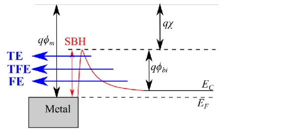
GaN. Furthermore at higher InN mole fraction, the valence band maximum (VBM) is shifted toward lower binding energy. I proposed a new approach to estimate the valence band maximum. I estimated a VBM of 2.1eV for GaN, which is more consistent with both the Schottky barrier height (SBH) and the build-in potential
evaluated at 1.2eV from C-V measurements. I estimated the band structures for InxGa1-xN materials depending on
the In content compared with the GaN band structure. For In0.09Ga0.91N compared with GaN, a band offset of 0.2
eV between the valence band maxima is present which can reduce the mobility of photogenerated carriers, especially for holes. To avoid any band offset for photo-generated carriers, a homojunction pn InGaN is thus more suitable.
Because of the larger observation depth of HX-PES, the spectra contain both surface and bulk information reflecting the band bending on the surface. By modifying the detection depth, the core level N1s was
shifted toward lower binding energy, underlining an upward band bending near the surface for GaN films [7]. I confirmed a shift of the core level N1s toward higher binding energy for InN films with a carrier concentration
lower than ~1.0×1018cm-3 for the first time, which underlines a downward band bending [8]. This downward band bending for the InN film can explain the difficulty in obtaining a Schottky junction by using this material. These results confirmed the importance of the band structure study for the interface and junction properties realized by using InxGa1-xN films.
3. Fabrication of Schottky junction and investigation of defect levels inside GaN and InGaN films
a. By using transparent conductive polymers
To demonstrate the photovoltaic effect of n-GaN and n-InxGa1-xN semiconductors, I fabricated a Schottky
junction device using a transparent conductive polymer (TCP). I employed two TCPs: PEDOT:PSS and polyaniline, because of their high electron affinity (about 5.2eV, which is the same as gold), their good conductivity and their high transmittance for the solar spectrum of about 80% from 300 to 1500 nm. These TCPs are known as p-type organic materials and are electrochemically stable conjugated polymers [9]. I elaborated a new contact structure on GaN or InxGa1-xN semiconductors, composed of the TCP and a thin Ti/Au front grid
(20/20nm) deposited by an e-beam evaporator. With such a structure, I realized the Schottky junction with excellent properties.
For the n-GaN semiconductor, I obtained the best Schottky barrier height (SBH) of 1.15eV with a low ideality factor of 1.3 using PEDOT:PSS and compared it with a Schottky junction that I fabricated using a thin gold layer of 70Å instead. By using the front contact structure, I obtained a larger surface area of about 0.40cm2 and good photovoltaic properties with an improved fill factor to about 0.70. For the InxGa1-xN semiconductors, I
could also observe the photovoltaic properties, but they were weak. Nevertheless, I observed an enhancement of the external quantum efficiency for a wider spectral range of 300 to 420nm for In0.11Ga0.89N compared with the
GaN material (300 - 375nm), which shows the potential of InxGa1-xN as an active layer in photovoltaic
applications.
Deep level optical spectroscopy (DLOS) analysis was performed on my best Schottky devices using n-GaN. The signal obtained by the DLOS analysis comes from the variation of the electric capacitance of Schottky junctions. The deep level defects are filled with electrons with a certain bias voltage applied and they are then released by monochromatic excitation without a bias applied. This variation of capacitance is an unique signature
of a specific defect inside the material bandgap. I underlined an enhancement of Ga cation vacancies (VGa) or
complexes associated with oxygen impurities (VGa-ON) and shallow carbon acceptors (CN) at the interface of the
TCP and n-GaN films [10]. Unfortunately the signal obtained was weak and the specimens could also contain defects inside the polymer itself. To analyze in detail the deep level defects inside n-InxGa1-xN, I fabricated thick
metallic contacts using Ti/Au layers (50/100 nm) and ohmic contacts using Ni/Au (50/100nm) deposited by an e-beam evaporator.
b. By using thick metallic contact
Until now there have been few reports concerning deep level defects in thick InxGa1-xN films. Those
defects could reduce the minority-carrier lifetime, increase the reverse saturation current and reduce the build-in potential of the junction in solar cells. In this work, thermal admittance spectroscopy (TAS), deep level transient spectroscopy (DLTS), and deep level optical spectroscopy (DLOS) were carried out for In0.09Ga0.91N films that I
deposited.
TAS measurement is a method that can detect defects located just below the conduction band (Ec). For
my In0.09Ga0.91N device, TAS revealed two defects at a level of Ec-7meV and Ec-108meV with low capture cross
sections. By applying a bias voltage (i.e. changing the depletion layer), the defect level of Ec-7meV appeared to be
homogeneously distributed in the InGaN layer, while the defects at Ec-108meV should be localized near the
surface. The first defect could be attributed to an indium fluctuation and / or nitride vacancies (VN), while the
second one could reveal the presence of an interface state between electrodes and InGaN layers.
DLTS measurements, which can analyze deeper defects between Ec and Ev, could underline two other
defects at Ec-22meV and Ec-0.6eV with a concentration of about 4×10 14
cm-3 for both of these defects. Because either TAS or DLTS technique could not explain the free carrier concentration of about 1.5×1017cm-3 present in the InGaN layer, DLOS analysis was also performed. I observed five photoemission states for In0.09Ga0.91N
detected at ~1.02 eV, ~1.70 eV, 2.07 eV (noted T3’), 2.70 eV, and ~3.05 eV (noted T5’) in addition to the near-band-edge emission of InGaN and GaN at 3.2-3.4 eV. Compared with the five photoemission states already observed for GaN films, which were identified at ~1.4 eV, ~1.7 eV (dislocation-related defect), ~2.1 eV [T3: Ga vacancies (VGa; the 2
-/3- transition level) and/or the VGa-ON complex] ~2.8 eV (VGa-CN complex), and ~3.05 eV
[T5: shallow acceptor carbon (CN)], the DLOS signal for the InGaN film was one order of magnitude higher. I
found that the defects T3’ and T5’ were remarkably enhanced when alloying InN with GaN [11]. These defects contribute to enhance the electron concentration (unintended n-doping) up to about 1017cm-3 for InxGa1-xN and
degrade the Schottky junction.
Therefore, to enhance the carrier lifetime and improve the junction quality, technological processes had to be developed to reduce or electronically passivate these deep level defects.
4. Photovoltaic properties of Schottky and p-n junctions of InxGa1-xN
The best photovoltaic conversion efficiency obtained by the p-i-n junction structure of InGaN materials is less than 2% [12], mainly because of the low crystal quality and the p-type doping. I successfully realized a homojunction p-n In0.10Ga0.90N revealing the following photovoltaic properties: the Voc is about 1.1 V and the Jsc
about 0.6 mA/cm2 with a fill factor of 62 %. To enhance the photovoltaic properties, an intrinsic layer i-InGaN was necessary. With a 150 nm-thick i-InGaN layer, the Voc obtained was about 2 V, the Jsc about 0.9 mA/cm
2
with a fill factor of 72 %.
To compensate the unintended n-type material behavior, I fabricated Schottky devices using a Mg-compensated InGaN layer on surface. During the rapid thermal annealing (RTA) of the ohmic and Schottky contacts, Mg atoms were activated and they compensated the unintended n-type InGaN. I achieved a Schottky junction with the following good properties: a Schottky barrier height of 1.18 eV, an ideality factor of 1.07, with a low leakage current density of 10-8 mA/cm2 at -4V bias. These enhanced properties clearly showed the ability of Mg to electronically compensate the defects present in the depletion layer of the Schottky junction. This fact may give a good perspective for future works to reach good p-n junction properties, because it is essential to know the diffusion profile of dopants inside the material. Indeed, secondary ion mass spectroscopy analysis revealed a high diffusion of Mg elements inside InGaN. A key point will be the precise control of the junction depth where the hole and electron concentrations are compensated for the realization of p-n homojunction InGaN.
To conclude, I have shown the capability of InGaN semiconductor for the photovoltaic application in this thesis. I successfully performed the analysis of the band structure and I revealed the presence of a band offset between the valence bands maximum of GaN and In0.09Ga0.91N films. After optimizing the growth condition for
InGaN epitaxial layers, I obtained promising photovoltaic properties of In0.11Ga0.89N by using Schottky junction
devices. This device had an extended solar-spectrum absorption from 300 to 430 nm. However the photovoltaic properties were limited because of the generation of defects when alloying InN into GaN. The main defects were successfully determined such as the cation vacancies (VGa and VN) and their complexes associated with oxygen or
carbon impurities. I found that the defects located below the conduction band at Ec-2.07 eV and Ec-3.05 eV were
easily introduced by alloying InN with GaN for In0.09Ga0.91N films. I also showed that the Mg-compensated
InGaN layer on the intrinsic InGaN film enhanced the Schottky junction properties and reduced the reverse leakage current.
However the photovoltaic conversion efficiency of our devices is still limited under 1%. After the determination of defects presented in this work, further studies still need to be done in order to reduce the concentration of these defects or to passivate them electronically. For instance, the development of a rapid thermal annealing depending on the temperature and the ambient gas used, such as nitrogen or oxygen, related with the junction properties can open a path to post-fabrication processes for defects passivation. It may be another very interesting study to establish the correlation between the luminescent defects observed by cathodoluminescence and the rapid thermal annealing step used to clarify some defect properties depending on the ambient gas.
The present study was successful in understanding the nature of defects generated, and the band structure of InGaN materials. It opens a path to future processes of defects passivation that will enhance the InGaN material quality for photovoltaic applications.
References of Abstract
[1] J. Wu, W. Walukiewicz, K. M. Yu, J. W. Ager, E. E. Haller, H. Lu, W. J. Schaff, Y. Saito, and Y. Nanishi, “Unusual properties of the fundamental band gap of InN,” Applied Physics Letters, vol. 80, no. 21, p. 3967, 2002.
[2] T. Nakao, T. Fujii, T. Sugiyama, S. Yamamoto, D. Iida, M. Iwaya, T. Takeuchi, S. Kamiyama, I. Akasaki, and H. Amano, “Fabrication of Nonpolar a-Plane Nitride-Based Solar Cell on r-Plane Sapphire Substrate,” Applied
Physics Express, vol. 4, no. 10, p. 101001, Oct. 2011.
[3] H. Amano, N. Sawaki, I. Akasaki, and Y. Toyoda, “Metalorganic vapor phase epitaxial growth of a high quality GaN film using an AlN buffer layer,” Applied Physics Letters, vol. 48, no. 5, p. 353, 1986.
[4] M. D. McCluskey, C. G. Van de Walle, C. P. Master, L. T. Romano, and N. M. Johnson, “Large band gap bowing of In x Ga 1 x N alloys,” Applied Physics Letters, vol. 72, no. 21, pp. 2725–2726, 1998.
[5] M. Smith, G. D. Chen, J. Y. Lin, H. X. Jiang, M. Asif Khan, and Q. Chen, “Time-resolved photoluminescence studies of InGaN epilayers,” Applied Physics Letters, vol. 69, no. 19, p. 2837, 1996.
[6] L. Sang, M. Takeguchi, L. Woong, Y. Nakayama, M. Lozac’h, T. Sekiguchi, and S. Masatomo, “Phase Separation Resulting from Mg Doping in p-InGaN Film Grown on GaN/Sapphire Template,” Applied Physics
Express, vol. 3, p. 111004, 2010.
[7] M. Sumiya, M. Lozac’h, N. Matsuki, N. Ohhashi, K. Sakoda, H. Yoshikawa, S. Ueda, and K. Kobayashi, “Valence band structure of III-V nitride films characterized by hard X-ray photoelectron spectroscopy,” Physica
Status Solidi (C), vol. 7, no. 7–8, pp. 1903–1905, 2010.
[8] M. Lozac’h, S. Ueda, S. Liu, H. Yoshikawa, S. Liwen, X. Wang, B. Shen, K. Sakoda, K. Kobayashi, and M. Sumiya, “Determination of the surface band bending in In x Ga 1− x N films by hard x-ray photoemission spectroscopy,” Science and Technology of Advanced Materials, vol. 14, no. 1, p. 015007, Feb. 2013.
[9] N. Matsuki, Y. Irokawa, Y. Nakano, and M. Sumiya, “Pi-Conjugated polymer/GaN Schottky solar cells,” Solar
Energy Materials and Solar Cells, vol. 95, no. 1, pp. 284–287, 2011.
[10] M. Lozac’h, Y. Nakano, L. Sang, K. Sakoda, and M. Sumiya, “Fabrication of transparent conducting polymer/GaN Schottky junction for deep level defect evaluation under light irradiation,” Physica Status Solidi
(a), vol. 210, no. 3, pp. 470–473, Mar. 2013.
[11] M. Lozac’h, Y. Nakano, L. Sang, K. Sakoda, and M. Sumiya, “Study of Defect Levels in the Band Gap for a Thick InGaN Film,” Japanese Journal of Applied Physics, vol. 51, p. 121001, Nov. 2012.
[12] Y. Kuwahara, T. Fujii, Y. Fujiyama, T. Sugiyama, M. Iwaya, T. Takeuchi, S. Kamiyama, I. Akasaki, and H. Amano, “Realization of Nitride-Based Solar Cell on Freestanding GaN Substrate,” Applied Physics, vol. 3, pp. 5–7, 2010.
Acknowledgments
I did my PhD study at National Institute for Materials Science (NIMS) in partnership with the University of Tsukuba thanks to the Doctoral Program in Materials Science and Engineering. I would like to acknowledge my Supervisor, Prof. Kazuaki Sakoda, Professor at the University of Tsukuba and Director of the Photonic Materials Unit at NIMS. I thank Prof. Sakoda who accepted me in his unit for his kind attention and numerous advices all along this work.
I acknowledge the Dr. Masatomo Sumiya who hosted me also in his group in the Environment and Energy Material Research Division inside NIMS, I wanted to thank him for his support, numerous advices and attention during my degree. I enter in contact with the Dr. Sumiya thanks to Prof. Etienne Gheeraert from the University Joseph-Fourier at Grenoble in France, so I wanted to thanks cheerfully Prof. Gheeraert here with Dr. Sumiya and Prof. Sakoda for the wonderful opportunity of doing my PhD study in Japan.
I am grateful for Prof. Takashi Sekiguchi, Prof. Naoki Futaka from NIMS, and Prof. Takeaki Sakurai of University of Tsukuba who accepted to form the graduation jury of my thesis. I thank these Professors very much for the great advices during my pre-defense.
I want to thank cheerfully Mrs. Kamisaka of Photonic Materials Unit and Mrs. Mabuchi of Environment and Energy Material Research Division who guided and helped me a lot through the different administrative procedures for NIMS, University of Tsukuba and my daily life. I also thank the International Student Center from the University of Tsukuba for all the useful information and accommodations.
All along my PhD study, I could meet and collaborate with many researchers in the group of Sumiya Sensei. I will remember all the moments we had together, especially with Fuke Sensei, Matsuki San, Ito San, Imura San, Mieno San, Akizuki San, Sang Liwen, Kubota San, Hanari San, Yamamoto San, Harada San, Ikeda San and Nakano San. I thank them all for the support, the advices along our work meetings and the very good times I had in their company during some dinners and events. I also thank Antoine Roehrich who brought a good ambiance and his “French touch” in our laboratory during his internship belong NIMS and the University of Grenoble (France) from May to August 2010.
From the group of Sakoda Sensei, I would like to thank Noda Sensei, Martin Elborg, and Yuanzhao Yao for their great discussions. It was a pleasure to meet them, and I will remember the good times passed together.
I also want to thank cheerfully all people who contribute and support me during my work at NIMS between Namiki and Sengen site: Benjamin Dierre, Tanaka Sensei, Elias Castel, Yiuri Garino, Ronit Prakash, Amir Pakdel, Martin Hollamby, Noelias Sanchez, Mehdi Estili, Komatsu Katsuyoshi, Julien Vieaud, Wim Van Rossom, Tanya Terentyeva, Marco Fronzi, Sara Romanazzo, Sun Yu, Noni Creasy, Lucie Szabova, Arnaud Le
Febvrier and Gaulthier Rydzek. They gave me many supports in different ways, and it was a great pleasure to share time and discuss together!
I acknowledge the professors from JST-ALCA project for supports and advices during this work: Nakano Sensei, Uedono Sensei, Honda Sensei and Hasegawa Sensei. More particularly, I am grateful to Nakano Sensei from Chubu University for the measurements and numerous discussions about defect levels.
I could make some measurements at AIST in collaboration with Dr. Koida San. I thank him for his time and support concerning the Hall effect measurement, the ITO deposition technique, the spectral response and the I-V simulator analysis.
Finally I want to thank all my friends I met in Tsukuba who directly or indirectly supported and motivated me during my PhD study. Tsukuba is a pretty small city and I saw a part of family in many of them. I wish all of them an accomplishment in their professional and personal life!
Last but not least, it is concerning my family. I spent a long time very far from my relatives, but I could feel a strong support and warm attention every time that I needed, so I thank them wholeheartedly! I send a special thanks to my brother who lives not so far in Tokyo. My last thoughts and thanks are for Kana the person who supported me the most and gave me the motivation during the hardest time of my thesis.
Table of contents
ABSTRACT ... I ACKNOWLEDGMENTS ... VIII TABLE OF CONTENTS ... X LIST OF FIGURES ... XIII LIST OF TABLES ... XVIII
1- INTRODUCTION AND PURPOSE OF RESEARCH ... 1
-1-1 GROWTH HISTORY OF GALLIUM NITRIDE (GAN), INDIUM NITRIDE (INN), AND THEIR ALLOY INGAN ... -2
-1-1.1 Gallium nitride (GaN) ... - 2 -
1-1.2 Indium nitride (InN) ... - 3 -
1-1.3 Indium gallium nitride (InGaN) ... - 4 -
1-2 ACTUAL STATUS OF HIGH EFFICIENCY SOLAR CELLS ... -5
-1-3 USE OF INXGA1-XN FILMS AS ACTIVE LAYERS FOR SOLAR CELL DEVICES ... -6
-1-3.1 Advantages of InGaN films ... - 7 -
1-3.2 Necessary conditions ... - 8 -
1-3.3 Application of InxGa1-xN films in solar cell structures ... - 10 -
1-3.4 Present solar cell structures using InGaN as an active layer ... - 12 -
1-3.5 Issues of InGaN films for photovoltaic application ... - 15 -
1-4 COMPOSITION OF THE THESIS ... -19
REFERENCES CHAPTER 1 ... 21
-2- FUNDAMENTAL PHYSICS FOR ELECTRONIC AND OPTICAL CHARACTERIZATIONS AND THIN FILM ANALYSIS TECHNIQUES ... 26
-2-1 PRINCIPLE OF PHOTOVOLTAIC CELLS AND PRESENTATION OF CRITICAL PARAMETERS ... -27
-2-1.1 Structure of solar cells and interaction between radiation and matter ... - 27 -
2-1.2 The p-n junction ... - 28 -
2-1.3 Electrostatic Characteristics ... - 32 -
2-1.4 Junction under polarization ... - 35 -
2-1.5 Electrical characteristics ... - 39 -
2-1.6 Equivalent electric circuit of solar cells ... - 41 -
2-1.7 Theoretical limit ... - 43 -
2-1.8 Recombination inside the material ... - 47 -
2-1.9 Moss-Burstein shift ... - 48 -
2-2 SCHOTTKY JUNCTION ... -50
-2-2.1 First discovery and introduction to Schottky diodes ... - 50 -
2-2.2 Early researches and theory about Schottky diodes (silicon case) ... - 51 -
2-2.3 Schottky contact on III-V nitride films ... - 52 -
2-2.4 Fundamental differences between Schottky and p-n junctions ... - 53 -
2-2.5 Current transport process inside Schottky junction ... - 54 -
2-2.6 Theoretical limit of the open-circuit voltage (Voc) for Schottky junction compared to p-n junction ... - 55 -
2-3 EQUIPMENTS FOR CHARACTERIZATION ... -56
2-3.2 Optical characterizations ... - 61 -
2-3.3 Electrics characterizations ... - 62 -
2-4 CONCLUSION ... -65
REFERENCES CHAPTER 2 ... 66
-3- MOCVD GROWTH TECHNIQUE AND OPTIMIZATION OF INXGA1-XN FILMS ... 69
-3-1 NITRIDE GROWTH TECHNIQUES ... -70
-3-1.1 Molecular Beam Epitaxy ... - 70 -
3-1.2 Vapor Phase Epitaxy ... - 70 -
3-1.3 Metalorganic Chemical Vapor Deposition ... - 70 -
3-2 DIFFERENT DEFECTS PRESENT IN A CRYSTAL ... -71
-3-2.1 Punctual defects ... - 71 -
3-2.2 Extended defects ... - 71 -
3-3 SAPPHIRE SUBSTRATE ... -72
-3-4 METALORGANIC CHEMICAL VAPOR DEPOSITION ... -73
-3-4.1 Recipe for InxGa1-xN film growth ... - 73 -
3-4.2 Role of the low temperature GaN as buffer layer (or nucleation layer) ... - 74 -
3-4.3 MOCVD reactor chamber ... - 75 -
3-4.4 Control of the flow of Metalorganic sources ... - 76 -
3-4.5 Control of indium composition ... - 79 -
3-4.6 Bandgap control and crystallinity ... - 83 -
3-4.7 Enhancement of electron mobility ... - 84 -
3-4.8 Magnesium as p-type doping for InGaN films ... - 86 -
3-4.9 Multi-layer (ML) structures ... - 86 -
3-4.10 Enhancement of the surface morphology... - 87 -
3-5 CATHODOLUMINESCENCE ANALYSIS ... -87
-3-6 CONCLUSION ... -91
REFERENCES CHAPTER 3 ... 93
-4- INVESTIGATION OF ELECTRONIC STRUCTURE FOR III-V NITRIDE THIN FILMS BY HARD X-RAY PHOTOEMISSION SPECTROSCOPY ... 94
-4-1 USE OF SPRING 8 FACILITIES FOR HARD X-RAY PHOTOEMISSION SPECTROSCOPY MEASUREMENT ... -95
-4-1.1 SPring 8 facilities... - 95 -
4-2 INVESTIGATION OF ELECTRONIC STRUCTURE FOR III-V NITRIDE THIN FILMS BY HARD X-RAY PHOTOEMISSION SPECTROSCOPY . -95 -4-2.1 Introduction ... - 97 -
4-2.2 Experimental details ... - 98 -
4-2.3 Core-level spectra of Ga 3d and In 4d for InxGa1-xN ... - 99 -
4-2.4 Surface band bending and VBM of GaN film ... - 100 -
4-2.5 N 1s core-level spectra of InN films grown by MBE ... - 101 -
4-2.6 VBM of InN films ... - 103 -
4-2.7 Conclusion ... - 104 -
REFERENCES CHAPTER 4 ... 106
-5- INVESTIGATION OF DEFECT LEVELS INSIDE GAN AND INGAN FILMS ... 109
-5-1 SCHOTTKY JUNCTION CHARACTERIZATION ON IN0.09GA0.091N THICK FILM ... -110
-5-1.1 Sample preparation ... - 110 -
5-1.2 Current-voltage measurement ... - 114 -
5-1.3 Capacitance-Frequency and capacitance-voltage measurements ... - 117 -
5-2 IN0.09GA0.91N DEFECT LEVELS STUDIED BY DEEP LEVEL TRANSIENT SPECTROSCOPY (DLTS) ... -119
5-2.2 Measurements using DLTS technique ... - 122 -
5-2.3 Analysis of DLTS measurements ... - 123 -
5-3 SHALLOW DEFECT LEVELS OF IN0.09GA0.91N ANALYZED BY THERMAL ADMITTANCE SPECTROSCOPY (TAS) TECHNIQUE ... -126
-5-3.1 Principle of the TAS technique ... - 126 -
5-3.2 Measurements using TAS technique ... - 131 -
5-3.3 Analysis of TAS measurements ... - 132 -
5-4 LOW ENERGY ACTIVATION OF DEFECTS RELATED TO DIELECTRIC RELAXATION ... -138
-5-5 DEEP LEVEL OPTICAL SPECTROSCOPY ... -139
-5-5.1 Principle of DLOS analysis ... - 139 -
5-5.2 Measurement using DLOS analysis ... - 140 -
5-5.3 Defect levels underlined by DLOS analysis ... - 140 -
5-6 CONCLUSION ... -142
REFERENCES CHAPTER 5 ... 144
-6- FABRICATION OF SOLAR CELL DEVICES AND PHOTOVOLTAIC PROPERTIES OF SCHOTTKY JUNCTION, P-N HOMOJUNCTION, AND P-I-N JUNCTION USING INXGA1-XN FILMS ... 147
-6-1 FABRICATION OF SCHOTTKY JUNCTION USING TRANSPARENT CONDUCTING POLYMERS ... -148
-6-1.1 Choice of the Transparent Conducting Polymers ... - 148 -
6-1.2 Fabrication process of transparent conducting polymer on GaN and InGaN films ... - 150 -
6-2 FABRICATION OF SCHOTTKY JUNCTION AND INVESTIGATION OF PHOTOVOLTAIC PROPERTIES OF THE GAN AND INGAN FILMS-154 -6-3 PHOTOVOLTAIC PROPERTIES OF P-N HOMOJUNCTION INXGA1-XN COMPARED TO P-I-N JUNCTION ... -160
-6-4 CONCLUSION ... -163
REFERENCES CHAPTER 6 ... 165
-7- CONCLUSIONS AND PERSPECTIVES ... 167
LIST OF PUBLICATIONS ... 170
-List of figures
FIG.1-1:CURRENT DENSITY ENGINEERING FOR EACH SUB-CELL TO MATCH THE SOLAR SPECTRUM FOR A THREE-JUNCTION
SOLAR CELL. ... -6
-FIG.1-2:SPECTRAL IRRADIANCE OF THE NORMALIZED SOLAR SPECTRUM AM1.5G, AND THE BANDGAP OF DIFFERENT SEMICONDUCTORS. ... -7
-FIG.1-3:EXPERIMENTAL VALUES [35] AND THEORETICAL CALCULATIONS [47] OF THE CRITICAL THICKNESS OF INXGA1-XN FILMS AS A FUNCTION OF THE INN MOLE FRACTION X FOR INGAN/GAN SINGLE-LAYER SYSTEM.EXPERIMENTAL RESULTS USED (0001) SAPPHIRE SUBSTRATE TO GROW A GAN EPILAYER (1ΜM) FOLLOWED BY INXGA1-XN GROWTH. ... -10
-FIG.1-4:STRUCTURE OF A FOUR-TERMINAL SOLAR CELL USING AN INXGA1-XN FILM ON THE TOP TO ABSORB THE SHORT WAVELENGTHS OF THE SOLAR SPECTRUM. ... -11
-FIG.1-5:THEORETICAL CONVERSION EFFICIENCY OF A FOUR-TERMINAL SOLAR CELL STRUCTURE USING AN INGAN FILM ON THE TOP [49]. ... -11
-FIG.1-6:EXAMPLE OF A MQW STRUCTURE USING I-INGAN AS ACTIVE LAYERS SEPARATED BY A GAN LAYER. ... -13
-FIG.1-7:EXAMPLE OF P-I-N JUNCTION STRUCTURE USING INGAN AS ACTIVE LAYER. ... -14
-FIG.1-8:EXAMPLE OF P-N HOMOJUNCTION STRUCTURE USING INGAN AS ACTIVE LAYER.... -14
-FIG.1-9:CROSS SECTIONAL SEM IMAGE OF INGAN/GAN FILM GROWN ON SAPPHIRE SUBSTRATE (SCALE 200 NM)[64]. ... -16
-FIG.1-10:ILLUSTRATION OF THE DEPLETION LAYER WIDTH WITH AND WITHOUT THE PRESENCE OF DEFECTS INSIDE. ... -17
-FIG.1-11:SCHEMA OF THE DEPLETION LAYER WIDTH WITH AND WITHOUT THE PRESENCE OF DEFECTS INSIDE. ... -18
-FIG.2-1:ILLUSTRATION OF THE OPERATING PRINCIPLE OF A SOLAR CELL. ... -28
-FIG.2-2:REPRESENTATION OF P-N HOMOJUNCTION AT THERMAL EQUILIBRIUM:(A) AND (B) INSIDE THE MATERIAL WITH THE FORMATION OF THE DEPLETION LAYER, AND (C) THE ELECTRONIC BAND STRUCTURE. ... -31
-FIG.2-3:THEORETICAL CALCULATION OF THE DEPLETION LAYER WIDTH W FOR GAN IN FUNCTION OF THE DONORS CONCENTRATION ND, THE ACCEPTOR CONCENTRATION NA IS FIXED AT 1016,1017,1018 AND 1019 CM-3AND THE TEMPERATURE AT 300K. ... -35
-FIG.2-4:CHARACTERISTIC CURRENT-VOLTAGE UNDER DARK CONDITION (DOTTED BLACK) AND UNDER ILLUMINATION (RED). . -39 -FIG.2-5:CHARACTERISTICS CURRENT-VOLTAGE (RED) AND POWER-VOLTAGE (BLUE) FOR A SOLAR CELL UNDER ILLUMINATION. ... -39
-FIG.2-6:EQUIVALENT ELECTRIC CIRCUIT OF SOLAR CELLS REPRESENTED BY A TWO-DIODE MODEL. ... -41
-FIG.2-7:CURRENT-VOLTAGE CHARACTERISTIC FOR ONE DIODE MODEL (LEFT) AND TWO DIODES MODEL (RIGHT). ... -42
-FIG.2-8:THE DIFFERENT NORMALIZED SOLAR SPECTRA ARE PRESENTED.AM0 SPECTRUM CORRESPONDS TO THE SOLAR SPECTRUM BEFORE THE ATMOSPHERE,AM1.5G THE SPECTRUM USED TO CHARACTERIZE THE SOLAR CELL ON THE GROUND LEVEL WITH SOME ABSORBED REGIONS DUE TO ELEMENTS CONSTITUTING THE ATMOSPHERE. ... -43
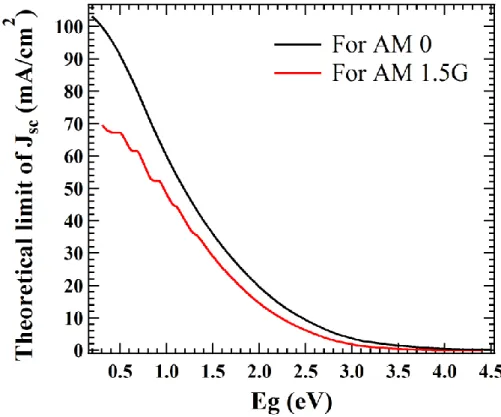
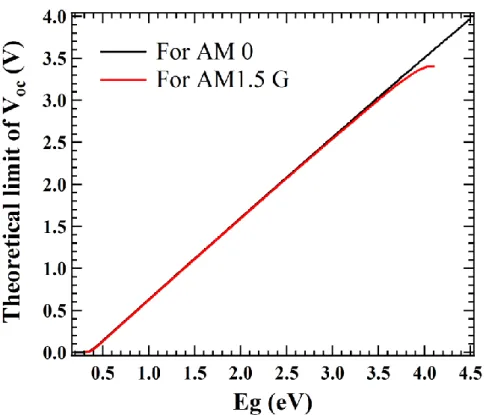
-FIG.2-9:THEORETICAL LIMIT OF THE CURRENT DENSITY DEPENDING ON THE MATERIAL BANDGAP (SUPPOSING A FULL ABSORPTION) UNDER NORMALIZED AM0 AND AM1.5G SOLAR SPECTRA. ... -44
-FIG.2-10:THEORETICAL LIMIT OF THE CURRENT DENSITY DEPENDING ON THE MATERIAL BANDGAP (SUPPOSING A FULL ABSORPTION) UNDER NORMALIZED AM0 AND AM1.5G SOLAR SPECTRA. ... -45
-FIG.2-11:THEORETICAL LIMIT OF THE CONVERSION EFFICIENCY CALCULATED FOR A FILL FACTOR OF 1(IDEAL CASE),0.85 AND (HIGHEST FILL FACTOR POSSIBLE) AND 0.75 UNDER NORMALIZED AM0 AND AM1.5G SOLAR SPECTRA.... -46
-FIG.2-12:ELECTRON MOBILITY OF GAN AT 77K(A) AND 300K(B) AS A FUNCTION OF CARRIER CONCENTRATION WITH COMPENSATION RATIOS, DENOTED NA/ND, OF 0,0.15,0.30,0.45,0.60,0.75, AND 0.90[11]. ... -48
-FIG.2-13:THEORETICAL DISPERSION CURVE OF VALENCE AND CONDUCTION BAND OF INN BY USING THE KP MODEL.THE FERMI LEVEL FOR N =1020 CM-3 IS REPRESENTED IN ORANGE [14]. ... -50
-FIG.2-14:ABSORPTION THRESHOLD (OPTICAL BANDGAP) IN FUNCTION OF ELECTRON CONCENTRATION.INN BANDGAP CALCULATED BY A DISPERSION CURVE OF THE PARABOLIC CONDUCTION BAND AND NON-PARABOLIC IS ALSO REPRESENTED [12]. ... -50
-FIG.2-15:CURRENT-VOLTAGE CHARACTERISTICS COMPARISON BETWEEN SCHOTTKY AND P-N DIODES. ... -54
-FIG.2-16:DIAGRAM OF A SCHOTTKY JUNCTION ON N-TYPE SEMICONDUCTOR REPRESENTING THE DIFFERENT REGIMES OF CURRENT TRANSPORT. ... -55
-FIG.2-17:ILLUSTRATION OF THE WURTZITE CRYSTAL STRUCTURE WITH THE C- AND A-LATTICE CONSTANTS, AND THE C-,A- AND M-PLANES. ... -57
-FIG.2-18:ILLUSTRATION OF THE DIFFRACTION GEOMETRY WITH THE DIFFERENT CRYSTALLINE PLANES OF THE SAMPLE AND THE ANGLES OF THE DIFFRACTOMETER USED. ... -57
-FIG.2-19:ILLUSTRATION OF THE CRYSTAL STRUCTURE FOR A STRAINED GROWTH MODE (A) AND A MORE RELAXED GROWTH MODE (B). ... -59
-FIG.2-20:MAPPING OF THE ( ) PLANE FOR IN0.07GA0.93N/ EPI-GAN STRUCTURE REPRESENTED IN RECIPROCAL LATTICES QX,QY TO ILLUSTRATE A STRAINED GROWTH MODE OF INGAN ON GAN. ... -59
-FIG.2-21:MAPPING OF THE ( ) PLANE FOR IN0.15GA0.85N/ EPI-GAN STRUCTURE REPRESENTED IN RECIPROCAL LATTICES QX,QY TO ILLUSTRATE A MORE RELAXED GROWTH MODE. ... -60
-FIG.2-22:SCHEMATIC PRINCIPLE OF AN ATOMIC FORCE MICROSCOPE (AFM). ... -61
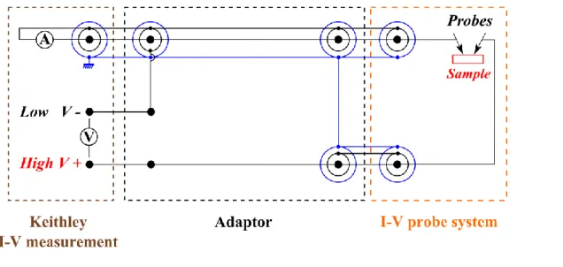
-FIG.2-23:ELECTRICAL CIRCUIT OF THE ADAPTOR FABRICATED BETWEEN THE I-V MEASUREMENT AND THE I-V PROBE SYSTEM WITH TRI-AXIAL CABLES CONNECTION. ... -63
-FIG.2-24:I-V CHARACTERISTIC OF TWO SCHOTTKY DEVICES USING THE PREVIOUS PROBES SYSTEM AND THE NEW I-V PROBES SYSTEM WITH THE ADAPTOR USING TRI-AXIAL CABLES CONNECTION. ... -64
-FIG.2-25:SOLAR SPECTRUM AM1.5G FROM 350 TO 800NM COMPARED TO THE XENON LAMP SPECTRUM WITH AND WITHOUT FILTER TO MATCH THE AM1.5G SPECTRUM. ... -65
-FIG.3-1:ILLUSTRATION OF DIFFERENT TYPE OF THREADING DISLOCATION: PURE EDGE (A), PURE SCREW (B), AND MIXED DISLOCATIONS (C). ... -72
-FIG.3-2:PROJECTION OF BULK BASAL PLANE SAPPHIRE AND GAN CATIONS POSITIONS FOR THE OBSERVED EPITAXIAL GROWTH ORIENTATION [7]. ... -73
-FIG.3-3:EXAMPLE OF DEPOSITION RECIPE USED FOR INXGA1-XN GROWN BY MOCVD. ... -74
-FIG.3-4:ILLUSTRATION OF THE BUFFER LAYER FORMATION AND THE CRYSTAL GROWTH. ... -75
-FIG.3-5:ILLUSTRATION OF THE MOCVD CHAMBER USED IN THIS WORK. ... -76
-FIG.3-6:PICTURE OF THE MOCVD EQUIPMENT USED TO DEPOSIT GAN AND INGAN FILMS. ... -76
-FIG.3-7:SYSTEM OF THE FLOWS FOR METALORGANIC SOURCES. ... -77
-FIG.3-8:EQUILIBRIUM VAPOR PRESSURE CURVES FOR TMGA,TMIN AND TMAL METALORGANIC SOURCES. ... -78
-FIG.3-9:CONTROL OF THE INN MOLE FRACTION DEPENDING ON THE TEMPERATURE FOR FOUR DIFFERENT GROWTH CONDITIONS A,B,C, AND D. ... -79
-FIG.3-10:FULL WITH AT HALF MAXIMUM (FWHM) OF THE INGAN PEAK FOR (0002) PLANE DEPENDING ON THE TEMPERATURE FOR FOUR DIFFERENT GROWTH CONDITIONS A,B,C, AND D. ... -80
-FIG.3-11:CONTROL OF THE OPTICAL BANDGAP BY THE INN MOLE FRACTION, C- AND A- LATTICES OF THE WURTZITE CRYSTAL ARE ALSO REPORTED DEPENDING ON THE INN MOLE FRACTION. ... -83
-FIG.3-12:TENDENCY OF THE ELECTRON MOBILITY OF INGAN FILMS AT DIFFERENT CARRIER CONCENTRATION DEPENDING ON THE INN MOLE FRACTION. ... -84
-FIG.3-13:TENDENCY OF THE ELECTRON MOBILITY OF INGAN FILMS AT DIFFERENT CARRIER CONCENTRATION DEPENDING ON THE INN MOLE FRACTION. ... -85
-FIG.3-14:TIME-RESOLVED PHOTOLUMINESCENCE FOR IN0.09GA0.91N AND GAN FILMS. ... -85
-FIG.3-15:IN0.09GA0.91N THICK FILM STRUCTURE DEPOSITED BY MOCVD ON C-PLANE SAPPHIRE SUBSTRATE. ... -86
-FIG.3-16:COMPARISON OF AFM IMAGE (55ΜM2) BETWEEN THE INGAN SURFACE IN EARLY DEVELOPMENT (A) AND THE INGAN WITH AN OPTIMIZED GROWTH CONDITION (B), BOTH STRUCTURES WERE ALSO ILLUSTRATED. ... -87
-FIG.3-17:CATHODOLUMINESCENCE ANALYSIS OF IN0.09GA0.91N WITH AN ELECTRON BEAM OF 10KV.(A)SECONDARY ELECTRON IMAGE AT A SCALE OF 5ΜM.(B)LUMINESCENCE OBSERVED AT 362 NM,(C) AT 388 NM,(D) AT 433 NM, AND (E) AT 550 NM. ... -88
-FIG.3-18:CATHODOLUMINESCENCE ANALYSIS FOR 10 POINTS OF IN0.09GA0.91N FILM. ... -88
-FIG.3-19:CATHODOLUMINESCENCE ANALYSIS OF A STRUCTURAL DEFECT IN0.09GA0.91N WITH AN ELECTRON BEAM OF 10KV. (A)SECONDARY ELECTRON IMAGE AT A SCALE OF 10ΜM.(B)LUMINESCENCE OBSERVED AT 362 NM,(C) AT 386 NM,(D) AT 430 NM, AND (E) AT 480 NM. ... -89
-FIG.3-20:CATHODOLUMINESCENCE ANALYSIS FOR 10 POINTS NEAR THE STRUCTURAL DEFECT ON SURFACE OF IN0.09GA0.91N
FILMS. ... -90
-FIG.3-21:CATHODOLUMINESCENCE ANALYSIS OF A STRUCTURAL DEFECT IN0.1GA0.9N WITH AN ELECTRON BEAM OF 10KV.(A)
SECONDARY ELECTRON IMAGE AT A SCALE OF 10ΜM.(B)LUMINESCENCE OBSERVED AT 362 NM,(C) AT 384 NM, AND (D)
AT 430 NM. ... -90
-FIG.3-22:CATHODOLUMINESCENCE ANALYSIS FOR 10 POINTS NEAR THE STRUCTURAL DEFECT ON SURFACE OF IN0.07GA0.93N
FILMS. ... -91
-FIG.4-1:SCHEMATIC ILLUSTRATION OF A BEAMLINE AT SPRING 8. ... -95
-FIG.4-2:(A)VALENCE BAND SPECTRA OF GAN AND INXGA1-XN FOR DIFFERENT INN MOLE FRACTIONS.(B)ILLUSTRATION OF
THE GAN BAND STRUCTURE REPRESENTING THE UPWARD BAND BENDING ON SURFACE. ... -96
-FIG.4-3:VALENCE BAND MAXIMUM OF GAN,INXGA1-XN(0<X<0.27), AND N-TYPE, P-TYPE DOPED FILMS. ... -96 -FIG.4-4:GA 3D,IN 4D,N2S CORE-LEVEL SPECTRA NORMALIZED BY THE INTEGRATED INTENSITY OF THE INXGA1-XN FILMS AT
TOA OF 88º. ... -99
-FIG.4-5:VALENCE BAND SPECTRA NORMALIZED BY THE INTEGRATED INTENSITY OF TYPICAL INXGA1-XN AND INN FILMS
OBSERVED BY HX-PES AT A TOA OF 88º. ... -100
-FIG.4-6:EXPANSION OF FIG.4-5 AT THE VALENCE BAND MAXIMUM.THE LINES ARE EXTRAPOLATED TO DETERMINE THE VBM.
... -101
-FIG.4-7:N1S CORE-LEVEL SPECTRA DETECTED AT TOAS OF 88 AND 30 FOR INN SAMPLES GROWN BY MBE WITH CARRIER CONCENTRATIONS OF (A)5.0×10¹⁷ CM-3,(B)1.5×10¹⁸ CM-3, AND (C)5.0×10¹⁸ CM-3.THE DASHED LINES ARE A GUIDE TO HIGHLIGHT THE VARIATION OF PEAK POSITION.THE INSETS SHOW ENERGY BAND DIAGRAMS EXPLAINING THE
RELATIONSHIP BETWEEN SURFACE BAND BENDING AND THE DETECTION DEPTH OF HX-PES, ALTHOUGH THE PROFILE FOR THE SURFACE OF INN REMAINS UNCLEAR. ... -102
-FIG.4-8: VALENCE BAND STRUCTURES DETECTED AT TOAS OF 88 AND 30 FOR INN FILMS WITH CARRIER CONCENTRATIONS OF (A)5×10¹⁸ CM-3 AND (B)5×10¹⁷ CM-3. ... -104
-FIG.5-1:IN0.09GA0.91N THICK FILM STRUCTURE DEPOSITED BY MOCVD ON C-PLANE SAPPHIRE SUBSTRATE. ... -110
-FIG.5-2:PICTURE OF TWO SCHOTTKY DEVICES DEPOSITED BY E-BEAM EVAPORATOR ON INGAN FILM ITSELF DEPOSITED ON
GAN EPILAYER / SAPPHIRE SUBSTRATE. ... -111
-FIG.5-3:XRD ANALYSIS OF IN0.09GA0.91N THICK FILM STRUCTURE FOR (0002) PLANE. ... -112
-FIG.5-4:TEM IMAGE OF THE IN0.09GA0.91N ON MULTI-LAYER STRUCTURE (ALN-GAN)10(SCALE 100NM). ... -112
-FIG.5-5:XRD MAPPING OF IN0.09GA0.91N THICK FILM STRUCTURE FOR ( ) PLANE REPRESENTED IN THE RECIPROCAL
SPACE. ... -113
-FIG.5-6:TEM IMAGE OF THE MULTI-LAYER STRUCTURE (ALN-GAN)10(SCALE 10NM). ... -113
-FIG.5-7:SURFACE OF THICK IN0.09GA0.91N FILM BY AFM MEASUREMENT FOR A 55 ΜM SCANNING AREA. ... -114
-FIG.5-8:CURRENT-VOLTAGE MEASUREMENT UNDER DARK CONDITION FOR THE SCHOTTKY PROPERTIES ON THICK
IN0.09GA0.91N FILM ... -116
-FIG.5-9:CAPACITANCE-FREQUENCY MEASUREMENT UNDER DARK CONDITION FOR THE SCHOTTKY PROPERTIES ON THICK
IN0.09GA0.91N FILM ... -118
-FIG.5-10:CAPACITANCE-VOLTAGE MEASUREMENT UNDER DARK CONDITION FOR THE SCHOTTKY PROPERTIES ON THICK
IN0.09GA0.91N FILM ... -118
-FIG.5-11:DLTS MEASUREMENT SYSTEM ... -123
-FIG.5-12:DLTS SPECTRA AT VARIOUS RATE WINDOWS FOR THE IN0.09GA0.91N SAMPLE ... -123
-FIG.5-13:ARRHENIUS PLOT OF THE DIP E2 FROM DLTS ANALYSIS OF THE IN0.09GA0.91N SAMPLE COMPARED TO DEFECT
LEVELS OF INGAN AND GAN IN REF.[15]. ... -124
-FIG.5-14:DLTSARRHENIUS PLOT OF THE DIP E1 FROM DLTS ANALYSIS OF THE IN0.09GA0.91N SAMPLE ... -125
-FIG.5-15:PARALLEL EQUIVALENT CIRCUIT OF A SCHOTTKY DIODE OR P-N JUNCTION. ... -126
-FIG.5-16:PRINCIPLE OF TAS TECHNIQUE, ENERGY DIAGRAM OF A SCHOTTKY BARRIER (N-TYPE SEMICONDUCTOR) WITH THE PRESENCE OF A DEFECT LEVEL ET. ... -127
-FIG.5-17:CALCULATED VARIATION OF THE CAPACITANCE CT, THE ADMITTANCE CT, AND THE CONDUCTANCE GT
ASSOCIATED WITH ONE TRAP DEPENDING ON THE FREQUENCY . ... -129
-FIG.5-18:CALCULATED VARIATION OF CT AND GT AS FUNCTIONS OF TEMPERATURE. ... -130
-FIG.5-20:CONDUCTANCE AND CAPACITANCE FOR IN0.09GA0.91N DEPENDING ON TEMPERATURE AND FREQUENCY AT 0V BIAS.
-133
-FIG.5-21:CONDUCTANCE (A) AND CAPACITANCE (B) FOR IN0.09GA0.91N DEPENDING ON TEMPERATURE AND FREQUENCY AT
-0.5V BIAS. ... -133
-FIG.5-22:CONDUCTANCE (A) AND CAPACITANCE (B) FOR IN0.09GA0.91N DEPENDING ON TEMPERATURE AND FREQUENCY AT
-1.0V BIAS. ... -133
-FIG.5-23:CONDUCTANCE (A) AND CAPACITANCE (B) FOR IN0.09GA0.91N DEPENDING ON TEMPERATURE AND FREQUENCY AT
-1.5V BIAS. ... -134
-FIG.5-24:CONDUCTANCE (A) AND CAPACITANCE (B) FOR IN0.09GA0.91N DEPENDING ON TEMPERATURE AND FREQUENCY AT
-1.5V BIAS. ... -134
-FIG.5-25:MAXIMUM CONDUCTANCE AT 15KHZ FREQUENCY IN FUNCTION OF THE BIAS VOLTAGE APPLIED FOR EACH PEAK A1, A2, AND A3 OBSERVED. ... -135
-FIG.5-26:CONDUCTANCE NORMALIZED BY THE FREQUENCY FROM 2 TO 100 KHZ FROM TAS MEASUREMENT. ... -136
-FIG.5-27:ARRHENIUS PLOT OF THE DEFECT LEVELS UNDERLINED BY TAS(A1,A2) AND DLTS(E1,E2) ANALYSIS FOR
IN0.09GA0.91N. ... -136
-FIG.5-28:EVOLUTION OF PEAKS DEPENDING ON BIAS VOLTAGE FROM -1V TO 2V FROM THE DEFECT LEVELS UNDERLINED BY
TAS ANALYSIS. ... -137
-FIG.5-29:ARRHENIUS PLOT OF THE DEFECT LEVELS UNDERLINED BY TAS(A1,A2) AND DLTS(E1,E2) ANALYSIS FOR
IN0.09GA0.91N COMPARED WITH DEFECT LEVELS FOR SI DOPED GAN. ... -138
-FIG.5-30:SCHEMATIC PRINCIPLE OF THE DLOS MEASUREMENT IN FOUR STEPS. ... -139
-FIG.5-31:DLOSMEASUREMENT SYSTEM ... -140
-FIG.5-32:DLOSSPECTRA MEASURED AT 0V BIAS CONDITION FOR INGAN(LEFT AXIS) AND GAN(RIGHT AXIS).FIVE DEFECT STATES DENOTED T1’–T5’ ARE CLEARLY OBSERVED IN ADDITION TO THE NEAR-BAND-EDGE (NBE) EMISSION OF INGAN
AND GAN AT 3.2–3.4EV. ... -141
-FIG.5-33:SUMMARY OF THE DEFECT STATES FOUND IN IN0.09GA0.91N FILMS BY USING THE TAS,DLTS AND DLOS
MEASUREMENTS. ... -143
-FIG.6-1:STRUCTURE OF POLYANILINE (PANI).(M, N)=(0.5,0.5) WITH 50% OF AMINE BONDS C-NH-C AND 50% OF IMINE BONDS C=N-C. ... -148
-FIG.6-2:CHEMICAL STRUCTURE OF PEDOT:PSS ... -149
-FIG.6-3:PRESENTATION OF THE DIFFERENT SPIN-COATING PROGRAMS USED TO DEPOSIT PANI AND PEDOT:PSS ON GAN
AND INGAN FILMS.... -151
-FIG.6-4:TRANSMITTANCE AND REFLECTIVITY OF A SINGLE LAYER OF PANI AND PEDOT:PSS DEPOSITED ON SAPPHIRE SUBSTRATE. ... -152
-FIG.6-5:EVOLUTION OF THE CONDUCTIVITY OF A PANI LAYER DEPENDING ON THE ANNEALING TEMPERATURE BY USING THE HOT PLATE UNDER AMBIENT AIR... -153
-FIG.6-6:EVOLUTION OF THE CONDUCTIVITY OF A PEDOT:PSS LAYER DEPENDING ON THE ANNEALING TEMPERATURE BY USING THE HOT PLATE UNDER AMBIENT AIR ... -153
-FIG.6-7:(A)SCHOTTKY PROPERTIES OF THE SCHOTTKY JUNCTION REALIZED BY PANI ON N-GAN AND N-IN0.11GA0.89N.(B)
SCHOTTKY PROPERTIES OF THE SCHOTTKY JUNCTION REALIZED BY PEDOT:PSS ON N-GAN AND N-IN0.09GA0.91N. . -155
-FIG.6-8:PHOTOVOLTAIC PROPERTIES OF SCHOTTKY SOLAR DEVICES USING PANI AND PEDOT:PSS ON N-GAN, N
-IN0.09GA0.91N AND N-IN0.11GA0.89N FILMS. ... -155
-FIG.6-9:(A)SCHEMATIC ILLUSTRATION OF THE NEW SCHOTTKY SOLAR CELL DEVICE USING METALLIC CONTACTS ON
PEDOT:PSS DEPOSITED ON GAN OR INGAN FILMS.(B)PICTURE OF ONE DEVICE, THE ACTIVE AREA IS ABOUT 0.41CM2. -156
-FIG.6-10:COMPARISON OF SCHOTTKY PROPERTIES USING PEDOT:PSS AND A THIN GOLD LAYER OF 70Å ON N-GAN .... -157
-FIG.6-11:COMPARISON OF PHOTOVOLTAIC PROPERTIES USING PEDOT:PSS AND A THIN GOLD LAYER OF 70Å ON N-GAN ... -157
-FIG.6-12:EVOLUTION OF THE OPEN-CIRCUIT VOLTAGE (VOC) AND THE SCHOTTKY BARRIER HEIGHT (SBH) OF THE DEVICE A1
IN FUNCTION OF TIME ... -158
-FIG.6-13:EXTERNAL QUANTUM EFFICIENCY OF SCHOTTKY SOLAR CELLS USING A SCHOTTKY JUNCTION REALIZED BY
-FIG.6-14:DLOS SPECTRA OF SCHOTTKY SOLAR CELL USING PEDOT:PSS/ N-GAN ON LEFT AXIS, AND USING AU (70Å)/N -GAN ON RIGHT AXIS. ... -160
-FIG.6-15:XRD ANALYSIS OF THE P-N IN0.1GA0.9N HOMOJUNCTION AND THE P-I-N IN0.1GA0.9N JUNCTION FOR (A)
(0002)-PLANE 2Θ-Ω SCAN, AND (B)( )-PLANE SCAN. ... -161
-FIG.6-16:SCHEMATIC STRUCTURE OF THE P-N HOMOJUNCTION AND P-I-N JUNCTION USING IN0.1GA0.9N FILMS. ... -161
-FIG.6-17:PHOTOVOLTAIC PROPERTIES OF THE HOMOJUNCTION IN0.1GA0.9N(IN RED) COMPARED TO P-I-N JUNCTION
IN0.1GA0.9N(IN BLUE). ... -162
-FIG.6-18:JUNCTION PROPERTIES UNDER DARK CONDITION FOR THE P-N HOMOJUNCTION AND P-I-N JUNCTION USING
-List of tables
TABLE 1-1:LATTICE CONSTANTS OF III-V NITRIDE CRYSTAL COMPARED WITH SAPPHIRE AT 300K. ... -8
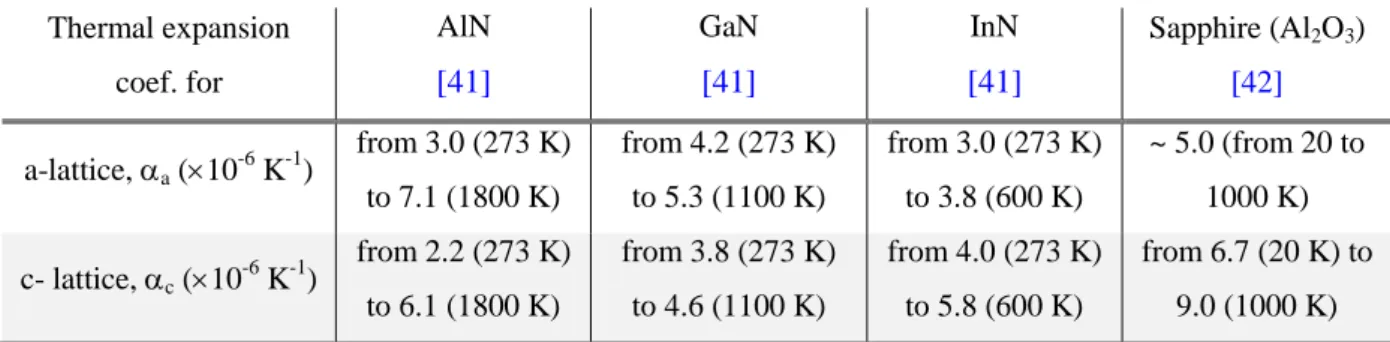
-TABLE 1-2:THERMAL EXPANSION COEFFICIENTS FOR A- AND C-LATTICE DIRECTION OF III-V NITRIDE CRYSTAL COMPARED WITH SAPPHIRE. ... -8
-TABLE 1-3:STATISTICAL VALUES FROM LITERATURE DATA WHICH PROVIDES COMPLETE EXPERIMENTAL OR THEORETICAL SETS OF THE STIFFNESS MATRIX ELEMENTS CIJ. ... -9 -TABLE 1-4:ACTUAL SITUATION OF SOLAR CELL STRUCTURES USING INGAN FILM AS ACTIVE LAYER.THE PHOTOVOLTAIC
PROPERTIES ARE PRESENTED WITH THE OPEN-CIRCUIT VOLTAGE (VOC), THE SHORT-CIRCUIT CURRENT (JSC), THE FILL
FACTOR (FF) AND THE CONVERSION EFFICIENCY (Η). ... -12
-TABLE 2-1:CARRIER DENSITY IN THE N-TYPE AND P-TYPE PARTS OF DOPED SEMICONDUCTOR... -30
-TABLE 2-2:EXPRESSION OF THE ELECTRIC FIELD E INSIDE THE DEPLETION LAYER.–XP AND XN ARE DEFINED AS THE BORDERS
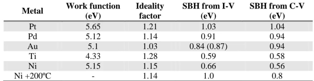
OF THE DEPLETION LAYER:-XP IN THE P-TYPE AREA, AND XN IN THE N-TYPE AREA (FIG.2-2) ... -33 -TABLE 2-3:SCHOTTKY BARRIER OBTAINED ON N-GAN GROWN ON SAPPHIRE SUBSTRATE USING DIFFERENT METAL DEPOSITED. .
-52
-TABLE 2-4:SCHOTTKY BARRIER OBTAINED ON N-GAN GROWN ON SIC SUBSTRATE USING DIFFERENT METAL DEPOSITED.... -53
-TABLE 3-1:LIST OF THE GROWTH CONDITION A PARAMETERS FOR INGAN FILMS GROWN BY MOCVD ... -80
-TABLE 3-2:LIST OF THE GROWTH CONDITION B PARAMETERS FOR INGAN FILMS GROWN BY MOCVD ... -81
-TABLE 3-3:LIST OF THE GROWTH CONDITION C PARAMETERS FOR INGAN FILMS GROWN BY MOCVD ... -81
-TABLE 3-4:LIST OF THE GROWTH CONDITION D PARAMETERS FOR INGAN FILMS GROWN BY MOCVD ... -81
-TABLE 3-5:SUMMARY OF THE FOUR GROWTH CONDITIONS USED TO DEPOSIT INXGA1-XN WITH DIFFERENT INN MOLE
FRACTIONS. ... -82
-TABLE 5-1:DIELECTRIC CONSTANT AND EFFECTIVE MASS OF ELECTRON FOR WURTZITE GAN,INN AND IN0.09GA0.91N AT 295K
-115
-TABLE 5-2:SCHOTTKY BARRIER HEIGHT AND IDEALITY FACTOR EXTRACTED FROM J-V ANALYSIS OF IN0.09GA0.91N AT 293K
DEPENDING ON THE EFFECTIVE MASS OF ELECTRON AND ON THE EFFECTIVE RICHARDSON CONSTANT USED. ... -117
-TABLE 5-3:DEFECTS LEVELS AND THEIR CHARACTERISTICS UNDERLINED BY DLTS FOR W-GAN WITH THEIR MAIN RELATED NATURES. ... -121
-TABLE 6-1:SCHOTTKY AND PHOTOVOLTAIC PROPERTIES OF GAN AND INXGA1-XN(X~0.10) FILMS BY USING PANI AND
PEDOT:PSS FOR THE SCHOTTKY JUNCTION. ... -154
-TABLE 6-2:SCHOTTKY AND PHOTOVOLTAIC PROPERTIES OF THE DEVICES A1 AND A2 OBSERVED INITIALLY AND AFTER 9
-Chapter 1
1- Introduction and Purpose of Research
1- INTRODUCTION AND PURPOSE OF RESEARCH ... 1
-1-1 GROWTH HISTORY OF GALLIUM NITRIDE (GAN), INDIUM NITRIDE (INN), AND THEIR ALLOY INGAN ... -2 -1-1.1 Gallium nitride (GaN) ... - 2 - 1-1.2 Indium nitride (InN) ... - 3 - 1-1.3 Indium gallium nitride (InGaN) ... - 4 -
1-2 ACTUAL STATUS OF HIGH EFFICIENCY SOLAR CELLS ... -5 -1-3 USE OF INXGA1-XN FILMS AS ACTIVE LAYERS FOR SOLAR CELL DEVICES ... -6 -1-3.1 Advantages of InGaN films ... - 7 - 1-3.2 Necessary conditions ... - 8 -
a) Crystal quality of IIIV nitride films ... 8 -b) Critical thickness of InGaN films ... 9
-1-3.3 Application of InxGa1-xN films in solar cell structures ... - 10 -
1-3.4 Present solar cell structures using InGaN as an active layer ... - 12 -
a) Multi quantumwell (MQW) structures ... 13 -b) pin junction structure... 13 -c) pn homojunction structure ... 14
-1-3.5 Issues of InGaN films for photovoltaic application ... - 15 -
a) Growth of thicker films ... 15 -b) GaN films and deeplevel defects associated ... 16 -c) Xray photoemission spectroscopy for band offsets and band alignments ... 17 -d) Schottky junction on InGaN films ... 18
-1-4 COMPOSITION OF THE THESIS ... -19 REFERENCES CHAPTER 1 ... 21
-It was recently proposed that the bandgap engineering of InxGa1-xN from 0.7 eV for InN [1] to 3.4 eV for
GaN [2], covering most of the solar spectrum, will allow III-V nitride semiconductors to be used in photovoltaic applications [3]. While the technology of light emitting diodes (LEDs) based on III-V nitrides is well established, the operation mechanism of solar cells is quite different from that of LEDs. In photovoltaic devices, the
absorption of solar light, the generation of photo carriers and their separation, transportation and collection are all crucial factors. High-quality thick InGaN films (0.2~0.3μm) are required to maximize the absorption. It is also necessary to analyze different brakes on the charge transport such as defects and the band structure. While InGaN films of several nm in thickness have been used as quantum-well layers in LEDs, the knowledge and study are needed to provide thicker InGaN films for photovoltaic applications. In the following, I describe the main parts for my study:
Deposition of thick InGaN films (0.2~0.3μm) with smooth surface, and control of the material bandgap with InN mole fraction in order to absorb enough solar light.
Analysis of point defects and deep-level defects in InGaN films in order to form better junctions. Evaluation of the band structure and band alignment depending on the InN mole fraction in order to
avoid a band offset affecting the carrier transportation at the interfaces between p-GaN/i-InGaN/n-GaN layers.
Realization of devices to analyze the photovoltaic properties of Schottky junction, p-n homojunction, and p-i-n junction using InGaN films.
In this study, I have improved the InxGa1-xN films and have evaluated both their electronic structures and
defects for the development of photovoltaic devices.
1-1 Growth history of gallium nitride (GaN), indium nitride (InN), and their
alloy InGaN
1-1.1 Gallium nitride (GaN)
Gallium nitride was firstly synthesized by Johnson et al. in 1932 [4]. In 1938 Juza and Hahn determined the crystal structure corresponding to the wurtzite structure [5]. In 1969, Maruska and Tietjen succeeded in growing GaN on a sapphire substrate by hybrid vapor phase epitaxy (HVPE) [2], and they clarified that GaN had a direct energy bandgap of 3.39eV.
Amano et al. achieved the first great advance in high-quality GaN growth by employing an AlN buffer layer (or nucleation layer) in 1986 [6]. The same team realized the second large progress in 1989 with the p-type doping control by using the bis-cyclopentadienylmagnesium (Cp2Mg) and the properties of the GaN p-n junction
LED were reported for the first time [7]. In this report, the characteristics of p-GaN were hole concentration of 2×1016cm-3, hole mobility of 8 cm2/Vs, and resistivity of about 35 Ωcm.
Thanks to the improvement in the deposition technologies like the Metalorganic Chemical Vapor Deposition technique (MOCVD, also called metalorganic Vapor Phase Epitaxy MOVPE) and the Hybrid Vapor Phase Epitaxy technique (HVPE), three groups succeeded in growing high-quality GaN in a short period. The first group was Amano et al. in 1990 [8] who made the first observation of the room-temperature stimulated emission near UV from a GaN film grown by MOCVD on a (0001) sapphire substrate using an AlN buffer layer. The
Chapter 1: Introduction and purpose of research
second group was Nakamura et al. [9] who realized a new MOCVD system with two different flows. One was an inactive gas perpendicular to the substrate to change the direction of the reactant gas flow. N-type materials had a carrier concentration and Hall mobility of 1×1018 cm-3 and 200 cm2/Vs, respectively. And the third group was Khan et al. in 1991 [10] who used low pressure MOCVD. The n-type GaN obtained had a carrier concentration and Hall mobility of about 1017 cm-3 and 350 cm2/Vs, respectively, at room temperature. Khan et al. were the first group to publish a report of UV sensors based on as-deposited single crystal insulating GaN films in 1992 [11].
1-1.2 Indium nitride (InN)
The first attempt to synthesize InN was made by Juza and Hahn in 1938 [5]. They obtained InN from InF6(NH4)3 and reported the crystal structure of InN to be wurtzite. Hovel and Cuomo had the earliest success in
the growth of InN with some good electrical properties in 1972 [12]. They obtained polycrystalline InN films with highly preferred orientation grown on sapphire and silicon substrates at 25-600ºC by reactive RF sputtering.
The previously reported large values of the bandgap, 1.8 – 2.0 eV, were explained by oxygen contamination and the Moss-Burstein shift [13], [14], which will be explained in Chapter 2, because of high electron concentration inherent to this semiconductor. More recently in 2002, J. Wu et al. reevaluated the bandgap of the InN to be about 0.7 eV [1] by growing high crystal-quality wurtzite-InN with an AlN buffer layer on sapphire substrates by molecular beam epitaxy (MBE). Lu et al. grew an high crystal-quality InN on a 200 nm-thick AlN buffer layer by MBE, which had a Hall mobility above 800 cm2/Vs and a low carrier concentration of 5×1018 cm-3 at 300 K [15]. Nanishi et al. obtained the same carrier concentration with a higher electron mobility of 1130 cm2/Vs at room temperature by using RF-molecular beam epitaxy [16].
Thanks to the InN bandgap reevaluation, the spectral range of nitrides covers from the UV with AlN (6.2 eV, corresponding to 200 nm) to the infrared with InN (0.7 eV, 1770 nm), and includes the near UV with GaN (3.4 eV, 364nm) and the visible range with their alloys, InGaN or AlInN. Thus, the research to use InGaN films as active layers for photovoltaic materials was advanced.
High-quality InN films were achieved in 2006 by Wang et al. They studied the polarity of InN films and reported high-quality N-polar InN films [17], and In-polar InN films grown by MBE [18]. For N-polar InN films grown on GaN template, they found that the growth behavior depends strongly on the growth temperature, which greatly influences the surface morphology. Step-flow-like morphologies and spiral growth were observed at temperatures higher than 540ºC with low dislocation density. The N-polar InN films grown at 470-600ºC had a residual electron concentration of 3.51018cm-3 with a Hall mobility of 1400 cm2 V-1 s-1 [17]. They also reported the step-flow mode growth for In-polar InN films on GaN template with a surface rms roughness less than 1nm over a 1010 μm2 area. After considering the surface electron accumulation layer on Hall electron concentration of 1.21018 cm-3, they estimated the residual electron concentration of bulk InN at about 5-61017cm-3. The Hall mobility was reported 1400 cm2 V-1 s-1. For these In-polar InN films, the FWHM of the (002) ω-scan was as small as 350 arcsec, which was close to that of the GaN template [18].
1-1.3 Indium gallium nitride (InGaN)
The InGaN films were deposited for the first time in 1972 by Osamura et al. with the technique of a plasma generated by electron beam on two different substrates, sapphire and quartz [19]. The layers were polycrystalline and the bandgap of InN was estimated at 1.95 eV, which means that the quality of the material fabricated was not so high.
In 1991, Yoshimoto et al. observed the first photoluminescence of In0.23Ga0.77N films grown on a (0001)
sapphire substrate at 800ºC by MOVPE [20]. Yoshimoto et al. studied the effect of growth conditions on the carrier concentration and transport properties of InxGa1-xN for an In composition 0.19 ≤ x ≤ 0.23. They observed
that if the deposition temperature was increased from 500 to 900ºC, InGaN films grown on (0001) sapphire had a reduction in the carrier concentration from 1020 to 1018 cm-3, but the carrier mobility was increased from less than 10 to 100 cm2V-1s-1 [20]. Yoshimoto et al. also observed that the indium mole fraction varied linearly with the group-III flow-rate ratio [TMI/(TMI+TEG)] ,where TMI stands for the flow-rate of trimethylindium and TEG for that of triethylgallium.
A major improvement of the InGaN film quality was obtained by Nakamura and Mukai in 1992 [21]. They discovered that the InGaN film quality could be significantly improved if a thick GaN epilayer (~2μm) is grown by MOCVD before the InGaN film on (0001) sapphire substrate. For the InGaN film deposition, Nakamura and Mukai used a temperature range between 830ºC to 780ºC with a high indium flow rate of 24μmol/min compared with the gallium flow rate of 2μmol/min. The indium content was 14 % at 830ºC and 24 % at 780 ºC.
Then, the InGaN films were developed for light emitting diodes (LEDs) with blue / green emission because of its bandgap variation depending on the indium mole fraction in an impressively fast way between 1990 and 2000 [22]. First high-brightness blue InGaN/AlGaN-double-heterostructure LEDs with a 500-Å-thick active layer of Zn-doped In0.06Ga0.94N were developed in 1993 [23] and then, blue/green InGaN single-quantum-well
(SQW) structure LEDs with a 30-Å-thick active layer of undoped In0.45Ga0.65N were developed in 1995 [24].
Other optical devices were also achieved such as the UV InGaN/AlGaN-double-heterostructure LEDs using a 400-Å-thick active layer of undoped InGaN with an In composition of nearly zero [25]. An amber InGaN single-quantum-well structure LEDs were achieved with a 25-Å-thick active layer of undoped InGaN [26]. The peak of the emission spectra was 594 nm, but the exact In composition was not determined due to weak signal intensity in X-ray diffraction and photoluminescence measurements. The first violet laser light emission at room temperature was achieved with an InGaN-based multi-quantum-well (MQW) structure [27]. The InGaN MQW structure consisted of 26 periods of 25-Å-thick In0.2Ga0.8N well layers and 50- Å-thick In0.05Ga0.95N barrier layers.
We should note that all these InGaN-based optical devices used very thin InxGa1-xN layers.
These InGaN-based LEDs were fabricated by MOCVD on (0001) sapphire substrate at atmospheric pressure using a GaN buffer layer (300~400 Å) and a GaN epilayer (3~4 μm) before the growth of InGaN-based structure or InGaN/AlGaN-based heterostructures. These growths used trimethylgallium (TMG), trimethylaluminium (TMA), trimethylindium (TMI), monosilane (SiH4), bis-cyclopentadienyl magnesium

![Fig. 1-5: Theoretical conversion efficiency of a four-terminal solar cell structure using an InGaN film on the top [49]](https://thumb-ap.123doks.com/thumbv2/123deta/8498774.922935/34.892.89.696.112.539/theoretical-conversion-efficiency-terminal-solar-structure-using-ingan.webp)
![Fig. 3-2: Projection of bulk basal plane sapphire and GaN cations positions for the observed epitaxial growth orientation [7]](https://thumb-ap.123doks.com/thumbv2/123deta/8498774.922935/96.892.119.803.116.513/projection-sapphire-cations-positions-observed-epitaxial-growth-orientation.webp)

