九州大学学術情報リポジトリ
Kyushu University Institutional Repository
低分子有機半導体薄膜のアモルファス構造制御と電 気・光物性
江﨑, 有
https://doi.org/10.15017/4060121
出版情報:Kyushu University, 2019, 博士(工学), 課程博士 バージョン:
権利関係:
2020 Doctor Thesis
Structural control of amorphous films of organic semiconductors and its effect on electrical and luminescence properties
Yu Esaki
Department of Chemistry and Biochemistry Graduate School of Engineering
Kyushu University
1
Contents
Chapter 1: Introduction………...4
1-1. Research background………..5
1-1-1. Organic light-emitting diodes………..5
1-1-2. Structure of organic films……….7
1-1-3. Structural control of polycrystalline films………8
1-1-4. Structural control of amorphous films………10
1-2. Research purpose and outline………14
References………16
Chapter 2: Enhanced electrical properties and air stability of amorphous organic thin films by engineering film density……….19
2-1. Introduction………...20
2-2. Results and discussion………...21
2-2-1. Film structure analysis………...21
2-2-2. Electrical properties………...30
2-2-3. Carrier transport model analysis………33
2-2-4. Air stability………36
2-3. Conclusion………39
References………40
Chapter 3: Discussion on hole traps of amorphous films of α-NPD deposited at different substrate temperatures………..43
3-1. Introduction………...44
3-2. Results and discussion………...44
3-2-1. Current enhancement in high-density films………...44
3-2-2. Theory of thermally stimulated current originating from bulk traps………...46
3-2-3. Thermally stimulated current and its origin………...…….49
2
3-2-4. Estimation of trap density………..53
3-2-5. Estimation of trap depth……….57
3-2-6. Discussion………..62
3-3. Conclusion………62
References………63
Chapter 4: Dependence of the amorphous structures and photoluminescence properties of Alq3 films on vacuum deposition conditions……….65
4-1. Introduction………...66
4-2. Experimental……….67
4-3. Results and discussion………...70
4-3-1. Film structure analysis………...70
4-3-2. Substrate-temperature dependence of photoluminescence properties………72
4-3-3. Deposition-rate dependence of photoluminescence properties………..74
4-3-4. Discussion………..76
4-4. Conclusion………77
References………78
Chapter 5: Effect of structural control of amorphous films on performance of organic light- emitting diodes………80
5-1. Introduction………...81
5-2. Experimental……….83
5-3. Results and discussion………...85
5-3-1. Displacement current measurement………...85
5-3-2. Current density–voltage properties………....89
5-3-3. External quantum efficiency………..91
5-3-4. Operational stability………...94
5-4. Conclusion………96
References………97
3
Chapter 6: Conclusion……….100
References………..103
Lists of symbols and abbreviations………104
Publication lists………..107
Acknowledgements………109
4
Chapter 1
Introduction
5 1-1. Research background
1-1-1. Organic light-emitting diodes
Organic light-emitting diodes (OLEDs) have attracted wide interests as next-generation displays and lighting devices. Since OLEDs based on a multilayered structure having a hole transport and a fluorescent organic emitter were reported by C. W. Tang et al. [1], OLED performance has been rapidly improved. However, internal quantum efficiency of classic fluorescent OLEDs is limited at 25% because radiative singlet excitons and non-radiative triplet excitons are formed in a 1:3 ratio after the recombination of electrons and holes injected from electrodes. To overcome this 25% limit, room- temperature phosphorescent emitters, such as iridium complexes, were developed [2]. With the phosphorescent emitters, internal quantum efficiency could be increased to ~100% because of the efficient intersystem crossing from the singlets to the triplets and the highly efficient phosphorescence from the triplets. In 2012, our group in Kyushu University discovered that thermally activated delayed fluorescence (TADF) is promising for achieving an internal quantum efficiency of 100% [3]. TADF- based organic emitters have a very small energy gap between the singlets and the triplets by carefully designing their chemical structures, leading to the efficient reverse intersystem crossing from the non- radiative triplets to the radiative singlets. Additionally, driving voltage and operational stability of OLEDs have also been improved by developing new organic semiconductor materials, device structures, and encapsulation technology. Thorough the comprehensive researches and developments in last 30 years, OLEDs are now on the commercialization stage.
Many advantages of OLEDs derive from the unique characteristics of organic materials. One is the flexibility of their chemical structures with different functionalities. This provides a wide range of the material choice for OLED fabrication. For OLEDs, several elastic films of organic materials are fabricated on a substrate, including a flexible plastic substrate, using simple vacuum deposition or solution process, making it possible to obtain light and flexible devices at a lower cost.
In OLEDs, holes and electrons are injected from electrodes and, then, recombine to form excitons for light emission. To carry holes and electrons efficiently, OLEDs are composed of several stacked organic films, each of which has an ability of hole transport, emission, or electron transport.
Because these films are very thin, each with a thickness of tens of nanometers, uniform and pinhole- free amorphous organic films are commonly used in OLEDs.
6
Typical strategies to improve OLED performance are a design of new organic materials which have higher carrier mobility and more efficient luminescence and an optimization of device structures considering energy levels of organics, a recombination zone, and light propagation paths. On the other hand, it has been revealed that the structural control of amorphous films is also effective for enhancing OLED performance [4–8]. An understanding of the relationship between amorphous film structures, electrical properties, and OLED performance is very important for establishing fundamental science and developing OLED industry. However, how film density affects OLED performance has not well been studied while controlling molecular orientation is known to be a key to improve OLED performances [4–7]. In this thesis, I performed a comprehensive study regarding both molecular orientation and film density. In this chapter, I introduce amorphous structures of organic films, their problems, and research backgrounds. Finally, I mention the research purpose and the outline of this thesis.
7 1-1-2. Structure of organic films
Electrical and luminescence properties of amorphous films of organic materials are determined by not only the nature of molecular structures but also their film structures. In other words, these properties can be controlled even in the same materials. Basically, films of low-molecular-weight organic materials are categorized into two types: polycrystalline films and amorphous films. Structural models of polycrystalline and amorphous films fabricated using a vacuum deposition process are shown in Fig. 1-1. Planar molecules have strong intermolecular interaction and tend to form polycrystalline films. There are macroscopic voids between crystallites and other crystallites or a substrate in polycrystalline films. On the other hand, bulky molecules having weak intermolecular interaction are difficult to form a crystal phase, resulting in the formation of films with a disordered amorphous state. In amorphous films, a number of microscopic voids (namely, free volume) exist.
These voids in polycrystalline and amorphous films would affect the film density; the larger amount of voids makes their film density low and causes the following problems:
(1) Voids work as carrier traps and energy barriers and, therefore, lower the carrier transport through films [9–11].
(2) Voids work as penetration paths for water and oxygen molecules and, therefore, lower the electrical and structural stability of films in air [12,13].
If these problems can be solved by removing voids from films through the optimization of vacuum deposition conditions, the electrical properties and stability of organic films would be enhanced.
Fig. 1-1. Structural models of (a) polycrystalline and (b) amorphous films of organic materials.
8 1-1-3. Structural control of polycrystalline films
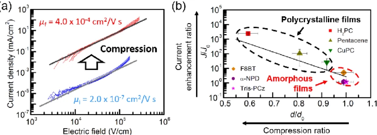
As one method to remove macroscopic voids in polycrystalline films, in my master thesis, I investigated the compression of organic films by applying high pressure using a cold isostatic pressing (CIP) method [14,15]. After the compression, the thicknesses of polycrystalline metal-free phthalocyanine (H2PC) films decreased by approximately 40%, indicating a removal of voids from films and an increase in film density. Figure 1-2(a) exhibits current density (J)–voltage (V) curves of as-deposited and CIP-treated H2PC films. Current densities were enhanced by three orders of magnitude after the compression in a whole voltage range, corresponding to a 2000-fold enhancement of hole mobilities. I found that this current enhancement was because of not only the rotation of crystallites to a direction in which carrier transport is more favorable, but also an improvement of the carrier conduction paths associated with a reduction of macroscopic voids. I carried out this CIP treatment on a wide variety of organic films. The current enhancement ratio increased as the compression ratio increased as shown in Fig. 1-2(b). All polycrystalline films were compressed by the CIP treatment and, therefore, their current densities were enhanced. The current enhancement was more significant when the compression ratio was higher. On the other hand, it was difficult to modulate the densities of amorphous films and improve their current densities using this CIP treatment.
Although the compression was not effective for the amorphous films, the aforementioned results proved that there was a clear relationship between the film densities and the current densities of polycrystalline films. Therefore, it is probable that the electrical properties of amorphous films are also improved if the film density can be increased using other methods.
9
Fig. 1-2. (a) Current density (J)–voltage (V) curves of as-deposited (blue lines) and CIP-treated (red lines) H2PC films and (b) relationship between the ratios of current densities J/J0 (current enhancement ratio) and film thicknesses d/d0 (compression ratio) before and after the CIP treatment. The structure of the devices was glass substrate/indium tin oxide (ITO)/organic layer/Al. These results were taken from my master thesis.
10 1-1-4. Structural control of amorphous films
Amorphous is a quasi-stable state as a result of kinetic relaxation of molecules. Although amorphous structures do not have a long-range ordering, it is misunderstanding that molecules are always random in amorphous systems. Since Lin et al. reported an optical anisotropy in vacuum- deposited amorphous organic films [16], many researchers started investigating the structures of amorphous films and developing methods to control amorphous structures.
Yokoyama et al. found that a variety of amorphous films of typical organic semiconductor materials showed optical anisotropy [17]. This anisotropy can be controlled by substrate temperature during vacuum deposition [18]. Because spin-coated films of organic materials are isotropic, this phenomenon is specific to a vacuum deposition process [19]. It was also confirmed that vacuum- deposited films exhibited higher thermal stability and density than spin-coated films and that these characteristics disappeared after annealing over the glass transition temperature of organic films [19].
Ediger et al. and several researchers also revealed a detailed film formation mechanism during vacuum deposition and named the vacuum-deposited amorphous films with high thermal stability, density, and anisotropy as “stable glasses” in contrast to “ordinary glasses” fabricated by liquid cooling or spin- coating [20–24].
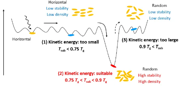
The key to obtain the stable glass films is a kinetics of molecules, namely, how each organic molecule moves and stops (stabilizes) on a film surface during film formation. The relationship between the kinetics of molecules and the final amorphous structure is summarized in Fig. 1-3. Note that the molecular orientation shown in the figure is valid for long-stick-shaped molecules. During vacuum deposition, molecules which reach the film surface do not stop immediately and move around until molecules find a stable position or are buried by next-coming molecules. This process sometimes looks like a famous video game “Tetris.” The motion of molecules can be understood considering a kinetic energy of molecules and explained by an energy landscape. Molecules can test many configurations and positions on the film surface, and each condition corresponds to a certain free energy. Although the number of states which molecules can take is very large because of the bulky and flexible molecular structures, the stable state with better packing (large enthalpic gain) is quite limited. Therefore, the energy landscape in Fig. 1-3 has many energetic valleys, but most of them are shallow. Because the structures of as-deposited amorphous films are the result of repeated relaxations,
11
the kinetics of molecules dominates the final film structure. There are three patterns of the relaxation processes concerning the kinetic energy of molecules, as summarized below. A substrate temperature (Tsub) during vacuum deposition can be used to control the kinetic energy. The conditions of Tsub
corresponding to these three patterns are also appended in the figure. The glass transition temperature (Tg) of ordinary glasses is typically used as a reference temperature because the glass transition reflects the relationship between a local molecular motion and a temperature.
Fig. 1-3. Energy landscape, molecular kinetics, and structural models of vacuum-deposited amorphous films of long-stick-shaped molecules.
(1) Too small kinetic energy (Tsub < 0.75 Tg):
Kinetic energy of molecules is not sufficient and the number of states which molecules can test is limited, so that most of molecules cannot find a deep valley position and stop in a shallow one.
The molecules have small enthalpic gain and inferior packing, resulting in low thermal stability and low density of amorphous films. Basically, the molecules orientate horizontally on the film surface to obtain enthalpic gain at the moment of landing.
(2) Suitable kinetic energy (0.75 Tg < Tsub < 0.9 Tg):
Kinetic energy of molecules is sufficient and molecules can test many states, so that molecules can stop in a deep valley position with a high probability. Therefore, the molecules obtain large
12
enthalpic gain and better packing, resulting in the formation of films with high thermal stability and high density. It is difficult for the molecules to maintain a horizontal orientation after a long- range migration. Thus, the molecules in amorphous films become random.
(3) Too large kinetic energy (0.9 Tg < Tsub):
Although molecules once find a stable position, they are released from there due to the excess kinetic energy and continue migration until molecules are buried by next-coming molecules. The molecules lack enthalpic gain and packing. This leads to low thermal stability and density of films. In this case, molecular orientation in amorphous films is slightly vertical relative to the substrate as a result of collisions of molecules and gradually approaches to no orientational order as Tsub increases to Tg.
It is known that the kinetic energy of molecules can be controlled by deposition conditions, such as Tsub and deposition rate. In this thesis, I mainly changed Tsub to fabricate films with different amorphous structures as a simple and most effective method. The range of Tsub used in this study corresponded to the three relaxation patterns as I mentioned earlier. The thermal stability and film density are known to exhibit the highest value around 0.75 Tg < Tsub < 0.9 Tg [case (2) in Fig. 1-3].
Molecules near the film surface are easier to move than those in the bulk. The Tg of the film surface is typically smaller than that of the film interior [25,26]. It is conceivable that Tsub which can provide the maximum thermal stability and film density corresponds to the Tg of the film surface.
While the mechanism of the amorphous film formation has been clarified to some extent, there are several studies regarding the effect of amorphous structures on the basic electrical properties and OLED performance. It has been reported that horizontal orientation of long-stick-shaped molecules on a substrate increases the transfer integral between adjacent molecules and, therefore, enhances carrier mobility in the substrate-normal direction [18]. Horizontal orientation of transition dipole moments of emitting molecules can increase light outcoupling efficiency [4]. The importance of controlling molecular orientation was experimentally confirmed in actual OLED structures [5–7]. In contrast, detailed study on how film density affects the electrical and photoluminescence (PL) properties and OLED performance has been lacked to date although enhanced photostability [27,28]
13
and improved external quantum efficiency and operational stability [8] with high-density amorphous films were reported.
Furthermore, vacuum-deposited amorphous films of organic molecules with large permanent dipole moment have strong polarization due to the anisotropic molecular orientation. This phenomenon is known as spontaneous orientation polarization (SOP) [29,30]. The SOP formation mechanism and the relationship to OLED performance have been investigated by comparing the degree of SOP in films of various materials with different molecular shapes and permanent dipole moments. If the SOP of single-material films can be controlled, a further discussion on the SOP formation mechanism and its influence on OLED performance would be possible.
14 1-2. Research purpose and outline
The main concept of this thesis is summarized in Fig. 1-4. Density and molecular orientation of amorphous films are controlled using Tsub during vacuum deposition to resolve the aforementioned problems and maximize the functionalities of organic materials. By increasing film density, I aim at improving the carrier conduction paths and suppressing the absorption of water and oxygen molecules into films, leading to the enhanced electrical properties and air stability. Formation of a thermally stable amorphous structure would result in the reduced crystallization and reorientation of molecules and the suppression of the film degradation during continuous operation. If OLEDs with extremely high air stability can be realized, the encapsulation widely used to protect devices from water and oxygen in air is no longer necessary, making a device fabrication cost lower. Furthermore, by tuning molecular orientation, not only the improvement of the light propagation paths but also the control of SOP in devices are expected. Through these studies, I aim at clarifying the detailed relationship between comprehensive amorphous structures (especially film density), fundamental electrical properties, and OLED performance, which is the originality of this thesis.
Fig. 1-4. Structural models of typical and optimized amorphous films of organic materials.
15
I briefly explain the outline of this thesis. In Chapter 2, I discussed the structure and electrical properties of amorphous films of a typical hole-transporting material, N,N'-di(1-naphthyl)-N,N'- diphenyl-(1,1'-biphenyl)-4,4'-diamine (α-NPD), controlled by Tsub during vacuum deposition. In Chapter 3, I evaluated carrier traps in α-NPD films using a thermally stimulated current method to clarify the origins of the current enhancement in the high-density films. In Chapter 4, I investigated the structure and PL properties of amorphous films of a typical electron-transporting and emitting material, tris(8-hydroxyquinolinato)aluminum (Alq3), controlled by Tsub and deposition rates. In Chapter 5, I fabricated OLEDs with α-NPD and Alq3 layers having different amorphous structures to prove how SOP induced by the molecular orientation affects OLED performance. In Chapter 6, I summarized main results of this thesis and mentioned future perspectives.
16 References
[1] C. W. Tang, S. A. VanSlyke, Organic electroluminescent diodes, Appl. Phys. Lett. 51, 913 (1987).
[2] M. A. Baldo, S. Lamansky, P. E. Burrows, M. E. Thompson, S. R. Forrest, Very high-efficiency green organic light-emitting devices based on electrophosphorescence, Appl. Phys. Lett. 75, 4 (1999).
[3] H. Uoyama, K. Goushi, K. Shizu, H. Nomura, C. Adachi, Highly efficient organic light-emitting diodes from delayed fluorescence, Nature 492, 234–238 (2012).
[4] W. Brütting, J. Frischeisen, T. D. Schmidt, B. J. Scholz, C. Mayr, Device efficiency of organic light-emitting diodes: progress by improved light outcoupling, Phys. Stat. Sol. A 210, 44–65 (2013).
[5] T. Komino, H. Nomura, T. Koyanagi, C. Adachi, Suppression of efficiency roll-off characteristics in thermally activated delayed fluorescence based organic light-emitting diodes using randomly oriented host molecules, Chem. Mater. 25, 3038–3047 (2013).
[6] T. Komino, H. Tanaka, C. Adachi, Selectively controlled orientational order in linear-shaped thermally activated delayed fluorescent dopants, Chem. Mater. 26, 3665–3671 (2014).
[7] T. Komino, Y. Sagara, H. Tanaka, Y. Oki, N. Nakamura, H. Fujimoto, C. Adachi, Electroluminescence from completely horizontally oriented dye molecules, Appl. Phys. Lett. 108, 241106 (2016).
[8] J. R. Ribé, P. A. Will, C. Hänisch, M. G. Silveira, S. Lenk, J. R. Viejo, S. Reineke, High- performance organic light-emitting diodes comprising ultrastable glass layers, Sci. Adv. 4, eaar8332 (2018).
[9] G. Horowitz, M. E. Hajlaoui, Mobility in polycrystalline oligothiophene field-effect transistors dependent on grain size, Adv. Mater. 12, 1046–1050 (2000).
[10] T. W. Kelley, C. D. Frisbie, Gate voltage dependent resistance of a single organic semiconductor grain boundary, J. Phys. Chem. B 105, 4538–4540 (2001).
[11] S. Seki, Y. Terashima, Y. Kunimi, T. Kawamori, M. Tashiro, Y. Honda, S. Tagawa, The effects of free volumes on charge carrier transport in polysilanes probed by positron annihilation, Radiat. Phys.
Chem. 68, 501–505 (2003).
[12] K. J. Dawson, K. L. Kearns, M. D. Ediger, M. J. Sacchetti, G. D. Zografi, Highly stable indomethacin glasses resist uptake of water vapor, J. Phys. Chem. B 113, 2422–2427 (2009).
[13] R. Surana, A. Pyne, R. Suryanarayanan, Effect of aging on the physical properties of amorphous trehalose, Pharm. Res. 21, 867–874 (2004).
[14] T. Matsushima, Y. Esaki, C. Adachi, Enhancement of the electrical characteristics of metal-free phthalocyanine films using cold isostatic pressing, Appl. Phys. Lett. 105, 243301 (2014).
17
[15] Y. Esaki, T. Matsushima, C. Adachi, Current enhancement in organic films through gap compression by cold and hot isostatic pressing, Adv. Funct. Mater. 26, 2940–2949 (2016).
[16] H.-W. Lin, C.-L. Lin, H.-H. Chang, Y.-T. Lin, C.-C. Wu, Anisotropic optical properties and molecular orientation in vacuum-deposited ter(9,9-diarylfluorene)s thin films using spectroscopic ellipsometry, J. Appl. Phys. 95, 881–886 (2004).
[17] D. Yokoyama, A. Sakaguchi, M. Suzuki, C. Adachi, Horizontal molecular orientation in vacuum- deposited organic amorphous films, Appl. Phys. Lett. 93, 173302 (2008).
[18] D. Yokoyama, Y. Setoguchi, A. Sakaguchi, M. Suzuki, C. Adachi, Orientation control of linear- shaped molecules in vacuum-deposited organic amorphous films and its effect on carrier mobilities, Adv. Funct. Mater. 20, 386–391 (2010).
[19] M. Shibata, Y. Sakai, D. Yokoyama, Advantages and disadvantages of vacuum-deposited and spin-coated amorphous organic semiconductor films for organic light-emitting diodes, J. Mater. Chem.
C 3, 11178–11191 (2015).
[20] S. F. Swallen, K. L. Kearns, M. K. Mapes, Y. S. Kim, R. J. McMahon, M. D. Ediger, T. Wu, L.
Yu, S. Satija, Organic glasses with exceptional thermodynamic and kinetic stability, Science 315, 353–
356 (2007).
[21] Y. Z. Chua, M. Ahrenberg, M. Tylinski, M. D. Ediger, C. Schick, How much time is needed to form a kinetically stable glass? AC calorimetric study of vapor-deposited glasses of ethylcyclohexane, J. Chem. Phys. 142, 054506 (2015).
[22] S. S. Dalal, D. M. Walters, I. Lyubimov, J. J. de Pablo, M. D. Ediger, Tunable molecular orientation and elevated thermal stability of vapor-deposited organic semiconductors, Proc. Natl. Acad.
Sci. 112, 4227–4232 (2015).
[23] A. Gujral, K. A. O’Hara, M. F. Toney, M. L. Chabinyc, M. D. Ediger, Structural characterization of vapor-deposited glasses of an organic hole transport material with X-ray scattering, Chem. Mater.
27, 3341–3348 (2015).
[24] J. Jiang, D. M. Walters, D. Zhou, M. D. Ediger, Substrate temperature controls molecular orientation in two-component vapor-deposited glasses, Soft Matter 12, 3265–3270 (2016).
[25] T. Komino, H. Nomura, M. Yahiro, C. Adachi, Real-time measurement of molecular orientational randomization dynamics during annealing treatments by in-situ ellipsometry, J. Phys. Chem. C 116, 11584–11588 (2012).
[26] S. S. Dalal, M. D. Ediger, Influence of substrate temperature on the transformation front velocities that determine thermal stability of vapor-deposited glasses, J. Phys. Chem. B 119, 3875–3882 (2015).
[27] Y. Qiu, L. W. Antony, J. J. de Pablo, M. D. Ediger, Photostability can be significantly modulated by molecular packing in glasses, J. Am. Chem. Soc. 138, 11282–11289 (2016).
18
[28] Y. Qiu, L. W. Antony, J. M. Torkelson, J. J. de Pablo, M. D. Ediger, Tenfold increase in the photostability of an azobenzene guest in vapor-deposited glass mixtures, J. Chem. Phys. 149, 204503 (2018).
[29] E. Ito, Y. Washizu, N. Hayashi, H. Ishii, N. Matsuie, K. Tsuboi, Y. Ouchi, Y. Harima, K. Yamashita, K. Seki, Spontaneous buildup of giant surface potential by vacuum deposition of Alq3 and its removal by visible light irradiation, J. Appl. Phys. 92, 7306–7310 (2002).
[30] Y. Noguchi, W. Brütting, H. Ishii, Spontaneous orientation polarization in organic light-emitting diodes, Jpn. J. Appl. Phys. 58, SF0801 (2019).
19
Chapter 2
Enhanced electrical properties and air stability of amorphous organic thin films by engineering film density
Y. Esaki, T. Komino, T. Matsushima, and C. Adachi The Journal of Physical Chemistry Letters 8, 5891–5897 (2017).
20 2-1. Introduction
Amorphous films composing OLEDs include microscopic voids originating from inefficient molecular packing. The presence of these voids are known to strongly limit charge-carrier injection and transport [1–3] and allow oxygen and water molecules to penetrate into organic films, causing the current–voltage properties and air stability of organic devices to deteriorate [4–6]. Some researchers have suggested that increasing the density of amorphous organic films results in lower moisture penetration [7,8]. In this thesis, I focus my attention on controlling Tsub during vacuum deposition of amorphous organic films to decrease the voids in films and increase the film density. If highly densified amorphous films can be obtained by controlling Tsub, these films should display enhanced electrical properties and air stability. In this chapter, I comprehensively investigate the influence of Tsub on the film density, molecular orientation, electrical properties, and air stability of amorphous α- NPD films. I reveal that an increase of film density achieved by controlling Tsub simultaneously leads to enhanced electrical properties and air stability. Although Tsub also controls the molecular orientation, molecular orientation has less influence than density on electrical properties and air stability of the α- NPD films.
21 2-2. Results and discussion
2-2-1. Film structure analysis
I used α-NPD purchased from Nippon Steel & Sumikin Chemical to fabricate films and devices because it is widely known to form amorphous films by vacuum deposition [9]. The chemical structure of α-NPD is shown in the inset of Fig. 2-4(a). For the measurements of density and molecular orientation, α-NPD films with a thickness of approximately 100 nm were vacuum-deposited on Si substrates kept at various Tsub ranging from 212 to 342 K. The Si substrates were pre-cleaned by ultrasonication in acetone, detergent, pure water, and isopropanol, followed by UV/O3 treatment. Tsub
was calibrated with an alumel/chromel thermocouple attached to the substrate surface beforehand. The pressure and deposition rate during the vacuum deposition of α-NPD were of the order of 10−4 Pa and 0.13 ± 0.03 nm/s, respectively. α-NPD films obtained at this Tsub range were in the amorphous state and had very smooth surfaces without pinholes. In contrast, α-NPD films fabricated at Tsub = 200 K were opaque and had large surface roughness. I speculate that water molecules condensed in the films during α-NPD deposition at this Tsub and then evaporated from films when Tsub was increased to room temperature after the deposition, which may result in the rough surface.
Variable angle spectroscopic ellipsometry (VASE; M-2000, J. A. Woollam) was performed on the vacuum-deposited α-NPD films on Si substrates to evaluate their molecular orientation, refractive index n, extinction coefficient k, and film thickness d. In the VASE measurements, the incident light angle ranging from 45° to 75° with a step of 5° and the spectral range was 245–1000 nm. As I discuss later, the molecular orientation evaluated by VASE changed markedly depending on Tsub, corresponding to a change of the transition dipole orientation of α-NPD molecules in the films. The transition dipole moment of α-NPD is known to be parallel to its long molecular axis [10]. The n and k spectra of organic semiconductor films are known to show anisotropy between the directions parallel
and perpendicular to the substrate plane because of the orientation of molecules, even in amorphous films [10–17]. Experimentally obtained Ψ and Δ curves were analyzed with an optical model considering uniaxial anisotropy based on an ordinary glass of α-NPD. The model was composed of Gaussian-type and Tauc–Lorentz-type oscillators to simultaneously obtain d values and spectra of n and k in each axis. The oscillator model parameters are shown in Table 2-1 and 2-2. Several examples of fitting results are presented in Fig. 2-1.
22 Table 2-1. Oscillator model parameters (Gaussian).
Oscillator type Amplitude Energy (eV) Breadth (eV)
Gaussian 1.0859 3.5807 0.53957
Gaussian 0.5599 4.444 0.84802
Gaussian 1.8865 5.6488 0.83336
Table 2-2. Oscillator model parameters (Tauc–Lorentz).
Oscillator type Amplitude Energy (eV) C (eV) Gap energy (eV)
Tauc–Lorentz 42.477 3.134 0.39286 2.944
23
Fig. 2-1. (a, c, e, g) Ψ and (b, d, f, h) Δ curves of α-NPD films vacuum-deposited at different Tsub. The experimental data (blue solid lines) was successfully fitted with the model (red dashed lines).
24
The accuracy of my optical model was confirmed by comparing the mean-squared error (MSE).
Figure 2-2 shows MSE values for α-NPD films vacuum-deposited at a Tsub of 212 K. The MSE showed the lowest value at a d of 88.474 nm. I chose this value as the real α-NPD thickness. When I increased or decreased the thickness parameter by 0.1 nm, the MSE value clearly rose as shown in this figure.
This result indicates that a small change of film thickness can be detected by my optical model.
Fig. 2-2. Plot of MSE values as a function of film thickness for an α-NPD film vacuum-deposited at a Tsub of 212 K.
25
The molecular orientation in each α-NPD film was then evaluated by calculating the orientation order parameter (S), which is defined as [14,16]:
𝑆 =3〈cos2𝜃𝑇𝐷𝑀〉−1
2 = 𝑘𝑧−𝑘𝑥
𝑘𝑧+2𝑘𝑥, (2-1)
where θTDM is the orientation degree of transition dipole moment of the molecules to the substrate- normal direction and kx and kz are the extinction coefficients in the directions parallel and perpendicular to the substrate plane, respectively.
For the measurement of relative film density (ρrel), α-NPD films were annealed under vacuum (< 1.0 × 10⁻³ Pa) for 30 min at 381 K after the first VASE measurements, and then cooled to room temperature at a certain rate. This annealing temperature was higher by about 20 K than the glass transition temperature of a bulk α-NPD film (Tg, bulk = 362 K) [11]. The thermal annealing is known to result in the formation of randomized molecular films with a certain density (ordinary glasses), the value of which is generally lower than that of as-deposited films, as reported previously [10,11,17].
Thus, the annealed films can be used as references to compare the density of the as-deposited films.
The annealed films were measured using VASE again. VASE after the annealing evidently indicated the randomization of α-NPD molecules accompanied with the change of optical parameters n and k and a slight increase of d in the annealed films compared with that before annealing. It should be noted that no obvious crystallization was observed in all films after the annealing. Assuming that the film area and the material weight on a substrate are unchanged before and after annealing, ρrel values are given by,
𝜌𝑟𝑒𝑙 =𝑑𝑑𝑎𝑛𝑛𝑒𝑎𝑙𝑒𝑑
𝑎𝑠−𝑑𝑒𝑝𝑜𝑠𝑖𝑡𝑒𝑑, (2-2)
where dannealed and das-deposited are the thicknesses of the annealed and as-deposited films, respectively.
26
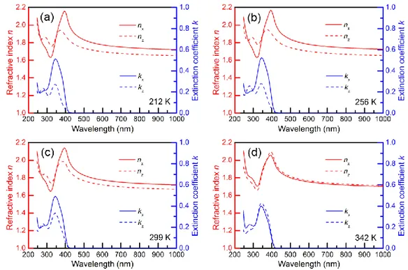
Figure 2-3(a–d) display the n and k spectra of α-NPD films vacuum-deposited at Tsub = 212, 256, 299, and 342 K. While nx and kx were similar to nz and kz for films vacuum-deposited at Tsub = 342 K, anisotropy of both n and k began to appear and became larger at low Tsub. The large anisotropy of the n and k spectra can be attributed to the anisotropy of the molecular orientation of α-NPD [10–
17].
Fig. 2-3. Refractive index n and extinction coefficient k spectra of representative α-NPD films vacuum-deposited on substrates kept at different substrate temperatures (Tsub) of (a) 212, (b) 256, (c) 299, and (d) 342 K.
27
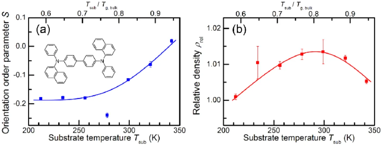
The S values estimated from the spectra at a wavelength of 344 nm using Eq. (2-1) are plotted as a function of Tsub in Fig. 2-4(a). Molecules (transition dipole moments) are vertically oriented, random, and horizontally oriented at S values of 1, 0, and −0.5, respectively. Therefore, the S value of nearly 0 for films vacuum-deposited at Tsub = 342 K indicates the randomization of α-NPD molecules.
The S value decreased as Tsub was lowered, indicating a gradual change from random to horizontal orientation of α-NPD molecules. Below Tsub ~250 K, the S values became almost constant. Similar Tsub-dependent orientations have been observed for other organic films [11–13].
The ρrel values at each Tsub, which were calculated from the change of d with Eq. (2-2), are plotted against Tsub in Fig. 2-4(b). I found that ρrel was a convex function of Tsub and that the maximum ρrel was between 270 and 300 K (0.75−0.83 Tg, bulk), which is close to a previous report [11].
Fig. 2-4. Plots of (a) orientation order parameter S and (b) relative density ρrel as a function of substrate temperature (Tsub) during vacuum deposition. The chemical structure of α-NPD is shown in the inset of (a).
28
To check the accuracy of the analysis, ρrel values were compared to those estimated from n of α-NPD films using the generalized Lorentz–Lorenz equation [11,17]:
〈𝑛2〉−1
〈𝑛2〉+2=4𝜋
3 𝑁𝐴𝛼
𝑀𝑤𝜌 ∝ 𝜌 (2-3) and
〈𝑛2〉 =2𝑛𝑥2+𝑛𝑧2
3 , (2-4)
where NA is the Avogadro constant, Mw is the molecular weight (588.74 g/mol for α-NPD), and α is the molecular polarizability. Figure 2-5 shows plots of ρrel values estimated from the change of d values and n values at a wavelength of 600 nm, where the films have no absorption, as a function of Tsub. The ρrel-Tsub plot estimated from n was found to be similar to that estimated from d.
Fig. 2-5. Plots of ρrel estimated from the film thicknesses d (red) and refractive indexes n (black) of α- NPD films as a function of Tsub. The red plot was taken from Fig. 2-4(b).
At low Tsub, the kinetic mobility of α-NPD molecules at a substrate surface is low, so molecules can move only a short distance and have a difficulty of finding an energetically stable position, leading to smaller ρrel. In contrast, at high Tsub, molecules have a sufficient kinetic mobility (a long enough molecular movement distance) to reach a more stable position, which provides better molecular packing, thereby resulting in higher ρrel. When Tsub was higher than about 0.8 Tg, bulk, ρrel decreased again. This would be because the excess kinetic mobility makes it difficult to keep molecules at a stable position. Thus, to obtain the highest ρrel, a substrate needs to be kept at about 0.8 Tg, bulk during the vacuum deposition of α-NPD films.
29
Here I discuss an increase of Tsub during vacuum deposition. It was reported that the radiant heat from a heated evaporation source does not affect the film morphology when the source temperature during vacuum deposition of α-NPD is around 570 K [18]. The deposited molecules orientate horizontally to obtain an enthalpic gain at the moment of landing, meaning that such a heating effect is sufficiently small not to destruct the film structure and randomize the horizontal orientation.
Although there is a possibility that this sort of heating effect increases the actual Tsub slightly, its effect on the film structure is assumed to be small. In fact, the Tsub is known to be increased by 1−2 ºC from room temperature when α-NPD is vacuum-deposited using a similar deposition system [19].
30 2-2-2. Electrical properties
I now examine how Tsub affects the electrical properties and air stability of α-NPD films considering the variations of S and ρrel. For this purpose, hole-only devices (HODs) containing an α- NPD layer were fabricated. The structure of the HODs was glass substrate/indium tin oxide (ITO) anode (100 nm)/α-NPD (about 350 nm)/MoO3 (30 nm)/Au cathode (50 nm). First, glass substrates coated with a 100-nm-thick ITO layer were cleaned using the method mentioned earlier. An α-NPD layer with a thickness of about 350 nm was vacuum-deposited on substrates kept at various Tsub under the conditions mentioned earlier. After Tsub was returned to room temperature, MoO3 and Au layers were vacuum-deposited on top of the α-NPD layer to complete the HODs. The active device area was 0.04 cm2. I used MoO3/Au as the cathode in the HODs because these layers are expected to be more stable in air than the Al and MgAg cathodes commonly used in OLEDs. Use of MoO3 with high work function suppressed electron injection in this structure [20,21]. Current density (J)–voltage (V) properties of HODs were measured with a computer-controlled sourcemeter (2400, Keithley) in nitrogen under the dark. I tried to precisely control the α-NPD film thickness at 350 nm using a quartz crystal microbalance installed near a substrate in a vacuum chamber. However, actual thicknesses showed a slight variation among films. Therefore, I used electric field E instead of V to allow better comparison of the film parameters. Here, E was calculated by simply dividing V by the α-NPD film thickness of each HOD measured using a profilometer (DEKTAK XT, Bruker).
31
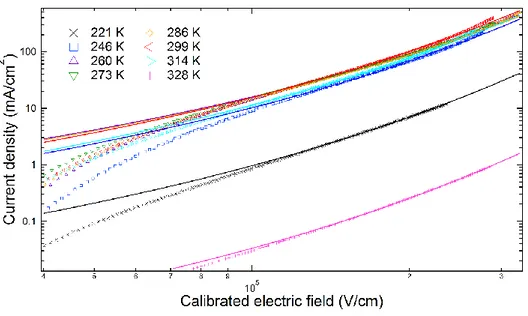
Figure 2-6(a) shows the J-E properties of the HODs. It was clear that the J-E properties were strongly affected by Tsub. Below about 3.0 × 10⁴ V/cm, I observed a bend in the J-E properties for the HODs except for those with α-NPD layers fabricated at Tsub = 314 and 328 K. I attributed this to an increase of carrier trap density, which will be discussed in the next chapter. The J values at an E of 1.0
× 105 V/cm without the influence of the bend are plotted as a function of Tsub in Fig. 2-6(b). J changes in a similar manner to that of ρrel in Fig. 2-4(b). Tsub where the maximum J was obtained was 260–290 K (0.72–0.80 Tg, bulk), which is not far from the results for ρrel [270–300 K (0.75–0.83 Tg, bulk)]. A higher ρrel indicates decreased intermolecular distance because the α-NPD molecules are packed more closely, which might be expected to enhance carrier transport in a film. In contrast, there was no clear relationship between J and S, even though it has been reported that the horizontal orientation of molecules on a substrate plane leads to enhanced carrier transport because of the better overlap of π orbitals between neighboring molecules in a substrate-normal direction [14]. There is a possibility that the density and orientation are different between films vacuum-deposited on ITO-coated glass substrates and Si substrates even at the same Tsub because of different substrate surface roughness [14].
Also, the molecular orientation might be different between the film surface and interior, which can change the energy level [22]. However, the substrate-dependent density and orientation and orientation-dependent energy level did not appear to be major factors here because J was strongly related to ρrel and not S. It should be noted that the ρrel and S values estimated by VASE here are the average values of the whole films. From the above results, I conclude that, for α-NPD, the film density has more influence on carrier transport than the molecular orientation does. Even though the ρrel
variation observed here is very small, just 1%–2%, the effect of ρrel on J is considerable, as can be seen in Fig. 2-6(b).
32
Fig. 2-6. (a) Representative current density (J)–electric field (E) properties of HODs with α-NPD layers vacuum-deposited at different substrate temperatures (Tsub) and (b) plot of J at E = 1.0 × 10⁵ V/cm versus Tsub.
33 2-2-3. Carrier transport model analysis
To gain insight into the observed increase of J, the J-E properties were analyzed with an injection-limited current (ILC) model, which can be given by [23–25]:
𝐽 = 4𝑁0𝜓2𝑒𝐸𝑒𝑥𝑝(−𝑒𝜙𝐵/𝑘𝐵𝑇)exp(𝑓0.5)𝜇(0)exp(𝛾𝐸0.5), (2-5)
where N0 is the density of chargeable sites in an organic film, e is the elementary charge, ΦB is the injection barrier height, kB is the Boltzmann constant, T is the temperature, μ(0) is the zero-field carrier mobility, γ is the Poole–Frenkel factor, f is the reduced electric field (𝑓 = 𝑒3𝐸/4𝜋𝜀0𝜀𝑟𝑘𝐵2𝑇2), ε0 is the vacuum permittivity, εr is the relative permittivity, and ψ is a function of f [𝜓 = 𝑓−1+ 𝑓−0.5− 𝑓−1(1 + 2𝑓0.5)0.5]. Here, N0 was assumed to be equal to the number density of α-NPD molecules in the films and could be obtained by the following equation:
𝑁0= 𝜌𝑎𝑏𝑠𝜌𝑟𝑒𝑙𝑁𝐴/𝜌𝑟𝑒𝑙,300𝐾𝑀𝑤, (2-6)
where ρabs is the absolute density of the films deposited at Tsub = 300 K (1.19 ± 0.01 g/cm3) [26], ρrel
is the relative film density, ρrel,300K is the relative density of the films deposited at Tsub = 300 K. The standard ɛr value of 3.0 and T of 300 K were used for the calculation. The work function of ITO was 5.0 eV and the ionization energy of α-NPD was 5.4 eV, both of which were measured by photoelectron yield spectroscopy (AC-3, RikenKeiki). Therefore, ΦB was estimated to be 0.4 eV. The HODs had a built-in potential (Vbi), which is probably defined by the difference between the work functions of ITO and MoO3 (5.0 and 5.9 eV, both measured by AC-3 spectroscopy). The electric fields of the HODs were calibrated with a Vbi value of −0.9 V using the relation: Ecalibrated = (V − Vbi)/d. Fitting was performed with μ(0) and γ as variables in the high voltage region, where the influence of the bend seems negligible. The fitting results are shown in Fig. 2-7.
34
Fig. 2-7. J-Ecalibrated properties of HODs with α-NPD layers vacuum-deposited at different substrate temperatures (Tsub). Solid lines are the fitting results of the ILC model used to estimate μ(0) and γ values.
Figure 2-8(a) and (b) show μ(0) and γ for which the best fitting results were obtained, respectively. The results revealed that the highest μ(0) and lowest γ appeared at 260–290 K (0.72–0.80 Tg, bulk), nearly agreeing with the Tsub values where the maximum ρrel was observed [270–300 K (0.75–
0.83 Tg, bulk)]. In films with higher density, the distribution of density of states (DOS) of molecules might be expected to be narrower because of the location of molecules at stable positions. This narrowing of DOS distribution can result in a lower barrier between neighboring states near the center of the distribution. The changes of tail states and state-to-state barriers probably led to a decrease of activation energy and enhanced rate of carrier hopping, which could be the origins of the increased μ(0) and decreased γ.
35
Fig. 2-8. Plots of (a) zero field mobility μ(0) and (b) Poole–Frenkel factor γ as a function of substrate temperature (Tsub) during vacuum deposition. The μ(0) and γ values were obtained by fitting the J-E properties in Fig. 2-6(a) with Eq. (2-5).
36 2-2-4. Air stability
After the J-V measurements, the air stability of HODs was evaluated from the temporal change of driving voltage under continuous current application at 0.1 mA/cm2 in air (without encapsulation) under the dark using an OLED lifetime measurement system (EAS-26B, System Engineers Co.). The temperature and relative humidity during the stability measurements were around 24 ºC and 50%, respectively.
The temporal changes of driving voltage are exhibited in Fig. 2-9(a). To make it easier to compare the temporal V changes among different HODs, the initial voltage (Vinitial) at 0 h in Fig. 2- 9(a) was offset to 0 V by subtracting Vinitial from V. For most of the HODs, V−Vinitial values increased monotonically over time. HODs with α-NPD vacuum-deposited at the lowest Tsub of 221 K showed a unique behavior; V−Vinitial values decreased during initial device operation and then began to increase rapidly; the reason for this behavior is still unclear and needs to be investigated in future. To quantitatively evaluate the air stability of the HODs from Fig. 2-9(a), slopes were calculated by dividing the difference in V−Vinitial between 0 and 300 h by the elapsed time of 300 h; the results are displayed in Fig. 2-9(b). In this figure, a smaller slope means higher air stability. The trend of air stability was a concave function with the minimum value at Tsub of around 270–300 K (0.75–0.83 Tg, bulk), consistent with the Tsub where the maximum ρrel was observed [270–300 K (0.75–0.83 Tg, bulk)].
These results reveal that α-NPD films with higher ρrel have higher air stability, while S has no relation to not only the electrical properties but also the air stability of the films. There is a possibility that S changes during the stability measurements. However, such a change of S should not markedly affect the stability results because carrier transport properties did not depend on S for α-NPD, as I discussed earlier.
37
Fig. 2-9. (a) Temporal changes of V for HODs with α-NPD layers vacuum-deposited at different Tsub. HODs were operated at a fixed current density of 0.1 mA/cm2 in air under the dark. The initial V at 0 h was offset to 0 V. (b) Slopes calculated by dividing the difference in V between 0 and 300 h by the elapsed time (300 h).
An increase of V under continuous operation of organic HODs may be caused by several factors, which include (1) degradation of metal electrodes [27], (2) decomposition of organic materials via excited states [28], (3) crystallization of amorphous films [6], and (4) absorption of gas molecules by films [4–8,29]. Factor (1) can be ruled out here because the ITO, Au, and MoO3 layers should be relatively stable in air and were used in all of the HODs discussed here. Also, factor (2) can be ignored because no excited state is formed by carrier recombination in the fabricated HODs [28]. It is expected that crystallization during device operation is likely suppressed for thermally stable films with high density. Optical microscopy revealed no marked α-NPD crystallization for all the HODs after 300 h of continuous operation. Thus, factor (3) is assumed not to be dominant. The factor (4) is a probable reason for the observed increase in V over time because the inclusion of water and oxygen into organic films accelerates degradation [4–6]. There are several reports describing film density being related to absorption of gas molecules [7,8,29]. Results in some reports [7,8] indicated that densification of organic films led to decreased water uptake, consistent with my present results. Conversely, water uptake decreased when Tsub was above room temperature, where the film density is expected to be lower, in another study [29]. Thus, how film density affects absorption of gas molecules (water uptake)
38
by films is still unclear. Based on my present results, air stability is undoubtedly enhanced with increasing film density. I speculate that the absorption of water and oxygen by the HODs operated in air was suppressed in high-density α-NPD films, and therefore the air stability was improved. The detailed roles of water and oxygen in the device degradation will be clarified in future.
39 2-3. Conclusion
In this chapter, I investigated the influence of Tsub during vacuum deposition of α-NPD films on their molecular orientation, film density, electrical properties, and air stability. I found that the electrical properties and air stability of the α-NPD films were most enhanced at Tsub of around 0.8 Tg,bulk. The reason for the enhanced electrical properties and air stability is mainly because of an increase of the film density at this Tsub and not a change of the molecular orientation. However, the aggregation-state change in the amorphous films, accompanied with the densification, is still unclear, and needs to be deeply clarified from a fundamental viewpoint. It is conceivable that there is a uniform decrease of intermolecular distance and that the spatial fluctuation of free volume in the films is lowered. While horizontal orientation is known to be very important to enhance the light outcoupling efficiency of OLEDs [30,31], it did not affect the electrical properties and air stability in this study. If horizontal orientation and high density can be achieved in the same film by controlling the chemical structures of organic materials and Tsub during their vacuum deposition, OLEDs with simultaneous higher external quantum efficiency, lower driving voltage, and higher air stability compared with conventional ones will be realized.
40 References
[1] G. Horowitz, M. E. Hajlaoui, Mobility in polycrystalline oligothiophene field-effect transistors dependent on grain size, Adv. Mater. 12, 1046–1050 (2000).
[2] T. W. Kelley, C. D. Frisbie, Gate voltage dependent resistance of a single organic semiconductor grain boundary, J. Phys. Chem. B 105, 4538–4540 (2001).
[3] S. Seki, Y. Terashima, Y. Kunimi, T. Kawamori, M. Tashiro, Y. Honda, S. Tagawa, The effects of free volumes on charge carrier transport in polysilanes probed by positron annihilation, Radiat.
Phys. Chem. 68, 501–505 (2003).
[4] T. Ikeda, H. Murata, Y. Kinoshita, J. Shike, Y. Ikeda, M. Kitano, Enhanced stability of organic light-emitting devices fabricated under ultra-high vacuum condition, Chem. Phys. Lett. 426, 111–114 (2006).
[5] F. Wölzl, I. R. de Moraes, B. Lüssem, S. Hofmann, K. Leo, M. C. Gather, Performance and lifetime of vacuum deposited organic light-emitting diodes: influence of residual gases present during device fabrication, Org. Electron. 15, 3251–3258 (2014).
[6] H. Aziz, Z. Popovic, S. Xie, A.-M. Hor, N.-X. Hu, C. Tripp, G. Xu, Humidity-induced crystallization of tris(8-hydroxyquinoline) aluminum layers in organic light-emitting devices, Appl.
Phys. Lett. 72, 756–758 (1998).
[7] K. J. Dawson, K. L. Kearns, M. D. Ediger, M. J. Sacchetti, G. D. Zografi, Highly stable indomethacin glasses resist uptake of water vapor, J. Phys. Chem. B 113, 2422–2427 (2009).
[8] R. Surana, A. Pyne, R. Suryanarayanan, Effect of aging on the physical properties of amorphous trehalose, Pharm. Res. 21, 867–874 (2004).
[9] T. Kato, T. Mori, T. Mizutani, Effect of fabrication conditions on photoluminescence and absorption of hole transport materials, Thin Solid Films 393, 109–113 (2001).
[10] Y. Sakai, M. Shibata, D. Yokoyama, Simple model-free estimation of orientation order parameters of vacuum-deposited and spin-coated amorphous films used in organic light-emitting diodes, Appl. Phys. Express 8, 096601 (2015).
[11] S. S. Dalal, D. M. Walters, I. Lyubimov, J. J. de Pablo, M. D. Ediger, Tunable molecular orientation and elevated thermal stability of vapor-deposited organic semiconductors, Proc. Natl. Acad.
Sci. 112, 4227–4232 (2015).
[12] A. Gujral, K. A. O’Hara, M. F. Toney, M. L. Chabinyc, M. D. Ediger, Structural characterization of vapor-deposited glasses of an organic hole transport material with X-ray scattering, Chem. Mater.
27, 3341–3348 (2015).
41
[13] J. Jiang, D. M. Walters, D. Zhou, M. D. Ediger, Substrate temperature controls molecular orientation in two-component vapor-deposited glasses, Soft Matter 12, 3265–3270 (2016).
[14] D. Yokoyama, Y. Setoguchi, A. Sakaguchi, M. Suzuki, C. Adachi, Orientation control of linear- shaped molecules in vacuum-deposited organic amorphous films and its effect on carrier mobilities, Adv. Funct. Mater. 20, 386–391 (2010).
[15] H.-W. Lin, C.-L. Lin, H.-H. Chang, Y.-T. Lin, C.-C. Wu, Y.-M. Chen, R.-T. Chen, Y.-Y. Chien, K.-T. Wong, Anisotropic optical properties and molecular orientation in vacuum-deposited ter(9,9- diarylfluorene)s thin films using spectroscopic ellipsometry, J. Appl. Phys. 95, 881–886 (2004).
[16] D. Yokoyama, Molecular orientation in small-molecule organic light-emitting diodes, J. Mater.
Chem. 21, 19187–19202 (2011).
[17] M. Shibata, Y. Sakai, D. Yokoyama, Advantages and disadvantages of vacuum-deposited and spin-coated amorphous organic semiconductor films for organic light-emitting diodes, J. Mater. Chem.
C 3, 11178–11191 (2015).
[18] T. Kato, T. Mori, T. Mizutani, Polarizing microscope observation for thin film of hole transport material -Effect of evaporation temperature and deposition rate-, T. IEE Japan 121-A, 672–676 (2001) [in Japanese].
[19] T. Matsushima, K. Shiomura, S. Naka, H. Murata, Optical, morphological, structural, electrical, molecular orientation, and electroluminescence characteristics of organic semiconductor films prepared at various deposition rates, Thin Solid Films 520, 2283–2288 (2012).
[20] M. Kröger, S. Hamwi, J. Meyer, T. Riedl, W. Kowalsky, A. Kahn, P-type doping of organic wide band gap materials by transition metal oxides: a case-study on molybdenum trioxide, Org. Electron.
10, 932–938 (2009).
[21] J. Meyer, S. Hamwi, M. Kröger, W. Kowalsky, T. Riedl, A. Kahn, Transition metal oxides for organic electronics: energetics, device physics and applications, Adv. Mater. 24, 5408–5427 (2012).
[22] W. Chen, W. H. Huang, S. Chen, Y. L. Huang, X. Y. Gao, A. T. S. Wee, Molecular orientation- dependent ionization potential of organic thin films, Chem. Mater. 20, 7017–7021 (2008).
[23] J. C. Scott, G. G. Malliaras, Charge injection and recombination at the metal–organic interface, Chem. Phys. Lett. 299, 115–119 (1999).
[24] Z. B. Wang, M. G. Helander, M. T. Greiner, J. Qiu, Z. H. Lu, Analysis of charge-injection characteristics at electrode-organic interfaces: case study of transition-metal oxides, Phys. Rev. B 80, 235325 (2009).
[25] Z. B. Wang, M. G. Helander, M. T. Greiner, J. Qiu, Z. H. Lu, Carrier mobility of organic semiconductors based on current-voltage characteristics, J. Appl. Phys. 107, 034506 (2010).
42
[26] H.-F. Xiang, Z.-X. Xu, V. A. L. Roy, C.-M. Che, P. T. Lai, Method for measurement of the density of thin films of small organic molecules, Rev. Sci. Instrum. 78, 034104 (2007).
[27] Y.-F. Liew, H. Aziz, N.-X. Hu, H. S.-O. Chan, G. Xu, Z. Popovic, Investigation of the sites of dark spots in organic light-emitting devices, Appl. Phys. Lett. 77, 2650–2652 (2000).
[28] D. Y. Kondakov, Role of chemical reactions of arylamine hole transport materials in operational degradation of organic light-emitting diodes, J. Appl. Phys. 104, 084520 (2008).
[29] J. M. Torres, N. Bakken, J. Li, B. D. Vogt, Substrate temperature to control moduli and water uptake in thin films of vapor deposited N,N'-di(1-naphthyl)-N,N'-diphenyl-(1,1'-biphenyl)-4,4'- diamine (NPD), J. Phys. Chem. B 119, 11928–11934 (2015).
[30] W. Brütting, J. Frischeisen, T. D. Schmidt, B. J. Scholz, C. Mayr, Device efficiency of organic light-emitting diodes: progress by improved light outcoupling, Phys. Stat. Sol. A 210, 44–65 (2013).
[31] T. Komino, H. Tanaka, C. Adachi, Selectively controlled orientational order in linear-shaped thermally activated delayed fluorescent dopants, Chem. Mater. 26, 3665–3671 (2014).
43
Chapter 3
Discussion on hole traps of amorphous films of α-NPD deposited at different substrate temperatures
Y. Esaki, T. Matsushima, and C. Adachi Applied Physics Letters 114, 173301 (2019).
44 3-1. Introduction
As I discussed in Chapter 2, I found that the hole current and air stability of amorphous films of α-NPD were the highest when Tsub during vacuum deposition was about 275 K [1]. This enhanced hole current was attributed to the decreased molecular distance and narrowing of DOS distribution in higher-density films deposited at this Tsub. However, there was a possibility that other factors also affected the electrical properties. In this chapter, I discuss the thermally stimulated currents (TSCs) of α-NPD films deposited at various Tsub. TSC measurements have been used to estimate the density and depth of carrier traps in inorganic, polymer, and small-molecule organic materials [2,3]. Analysis of the TSC results reveals that hole traps exist in bulk films and are the shallowest when films are deposited at the optimized Tsub of around 275 K.
3-2. Results and discussion
3-2-1. Current enhancement in high-density films
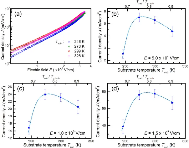
For measurements of electrical properties and TSCs, I first fabricated HODs with the same structure used in Chapter 2. However, the obtained TSC signals were too noisy, probably due to small leakage currents caused by diffusion of Au atoms into α-NPD. Therefore, I replaced the Au cathode with Al for reliable TSC measurements. The new HOD structure was glass substrate/ITO anode (100 nm)/α-NPD (300 nm)/MoO3 (30 nm)/Al cathode (50 nm). α-NPD was deposited on the substrate kept at various Tsub ranging from 240 to 330 K to form a film with a thickness of 300 nm. After α-NPD deposition, Tsub was returned to room temperature and then MoO3 (30 nm) and Al cathode (50 nm) layers were vacuum-deposited on the α-NPD layer. After the J-E properties were obtained, HODs were encapsulated using a glass cap and UV curing epoxy resin in the nitrogen-filled glove box to avoid degradation of the films in air during TSC measurements. The detailed conditions of the vacuum deposition and the J-E measurement were the same as those in Chapter 2.
45
I first confirmed whether the current enhancement was correctly reproduced in the new HODs.
J-E properties of the new HODs fabricated with different Tsub are shown in Fig. 3-1(a). J values taken from these curves at an E of 5.0 × 10⁴, 1.0 × 10⁵, and 1.5 × 10⁵ V/cm are plotted versus Tsub in Fig. 3- 1(b−d). At every E, J values strongly depended on Tsub and were the highest at a Tsub of around 275 K (~0.75 Tg,bulk), consistent with the result obtained in Chapter 2 [1].
Fig. 3-1. (a) Representative current density (J)–electric field (E) curves of HODs fabricated at various substrate temperatures (Tsub) during vacuum deposition. (b–d) Plots of J values at an E of (b) 5.0 × 10⁴, (c) 1.0 × 10⁵, and (d) 1.5 × 10⁵ V/cm as a function of Tsub for HODs fabricated at Tsub = 246, 273, 299, and 328 K. The dashed lines are guides to the eye.