Structural and photoluminescence properties of porous GaP formed
by electrochemical etching
Katsuhiro Tomioka and Sadao Adachia兲
Department of Electronic Engineering, Faculty of Engineering, Gunma University, Kiryu-shi, Gunma 376-8515, Japan
共Received 27 May 2005; accepted 29 August 2005; published online 5 October 2005兲
The structural and optical properties of porous GaP have been studied by scanning electron microscopy, spectroscopic ellipsometry, and photoluminescence 共PL兲 spectroscopy. Porous GaP layers were fabricated by anodic etching in HF : H2O : C2H5OH = 1 : 1 : 2 electrolyte on n-type共100兲 and共111兲A substrates. The morphology of the porous GaP layer is found to depend strongly on the surface orientation. Apart from the red emission band at⬃1.7 eV, a supra-band-gap 共Eg
X兲 emission
has been clearly observed on the porous GaP共111兲A sample. The anodic porous layer on the 共100兲 substrate, on the other hand, has shown only the red emission at 300 K and both red and green donor-acceptor pair emissions at low temperatures. The correlation between the PL properties and the porous morphology is discussed. An optical transition model is also proposed for the explanation of the PL emission properties of the porous GaP samples. © 2005 American Institute of Physics. 关DOI:10.1063/1.2076445兴
I. INTRODUCTION
Porous semiconductors have received much attention since the observation of visible room-temperature lumines-cence from porous silicon.1 The anodic technique has been used for several decades now and has proved to be a useful nanofabrication tool in the synthesis of porous structures.2–4 Like silicon, compound semiconductors such as GaP and GaAs have been investigated in the form of porous structures and many different properties relative to those of bulk mate-rials have been reported. For instance, UV and visible emis-sions have been observed in the porous layers of GaP,5–7 GaAs,8,9 and InP.10–12 Stable field electron emitters have been fabricated using porous GaP and GaAs layers.13,14A large birefringence has also been observed in porous GaP and InP, allowing phase matching for second-harmonic generation.15
Our aim in this paper is to present data concerning the structural and optical properties of porous GaP formed on 共100兲 and 共111兲A substrates by anodic etching. In silicon,3,16 the pores tend to grow in 具100典 directions. With increasing anodic voltage, the 具100典 directions become more dominat-ing for the side pores as well. The pore formation in silicon is, therefore, an anisotropic process. Various n-type com-pound semiconductors have also been fabricated as porous structures on共100兲 substrates by electrochemical etching. No surface orientation dependence has, however, been consid-ered in these studies. Here, we form porous structures not only on the共100兲 substrate, but also on the 共111兲A substrate and compare their structural and optical properties by a scan-ning electron microscopy共SEM兲, spectroscopic ellipsometry 共SE兲, and photoluminescence 共PL兲 spectroscopy. An inter-band transition model is proposed for the explanation of PL emission properties in anodically formed porous GaP samples.
II. EXPERIMENT
The samples used in this study were n-type, sulfur-doped GaP with 共100兲 and 共111兲A surface orientations. They were doped with a sulfur donor density of ⬃3⫻1017 cm−3. The porous layers were fabricated by anodic etching of GaP wa-fers in an electrochemical cell. The electrolyte used was a 46% solution of HF in deionized water and methanol with a volume ratio of HF : H2O : C2H5OH = 1 : 1 : 2. The etching pro-cess was performed by illuminating a light from a 100 W xenon lamp at room temperature for t = 10, 30, and 60 min at a current density of 20 mA/ cm2.
The anodized GaP layer was evaluated by SEM. The automatic ellipsometer was of the polarizer-sample-rotating-analyzer type 共DVA-36VW-A, Mizojiri Optical兲. A 150 W xenon lamp was used as a light source. The SE measure-ments were carried out in the 1.5– 5.4 eV photon-energy range at room temperature. The angles of incidence and po-larizer azimuth were set at 45° and 40°, respectively.
PL measurements were performed using a grating spec-trometer共Jasco CT-25C兲 and a Peltier-device-cooled photo-multiplier tube 共Hamamatsu R375兲. The 325 nm line of a He–Cd laser共Kimmon IK3302R-E兲 chopped at 328 Hz was used as the excitation light source. The measurements were performed using a closed-cycle refrigerator cryostat共Iwatani CRT105PL兲 at T=15–300 K.
III. RESULTS AND DISCUSSION
A. Scanning electron microscopy observation
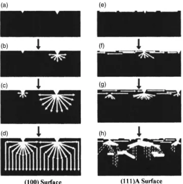
We show, in Figs. 1 and 2, SEM images of the porous GaP layer formed on the 共100兲 substrate by anodic etching for t = 10 and 30 min, respectively. The SEM images of a porous GaP formed on the共111兲A substrate for t=30 min are also shown in Fig. 3. In accordance with these SEM images, we depict in Figs. 4共a兲–4共h兲 the possible anodic etching pro-cesses on the GaP共100兲 and 共111兲A substrates, respectively.
a兲Electronic mail: [email protected]
JOURNAL OF APPLIED PHYSICS 98, 073511共2005兲
At the beginning of the GaP共100兲 process, the etching starts at surface imperfections 关Fig. 4共a兲兴.17,18 After initial pitting of the surface, further etching proceeds in all direc-tions radically away from the initial surface imperfection 关Figs. 4共b兲 and 4共c兲兴. As a result, a porous domain is formed around each etch pit. The pores in each domain distinctly grow perpendicular to the equipotential lines of the electric field in the anodized specimen. Since the etching proceeds at the same rate in all directions, the boundary of the porous
region, that is, the porous domain, is circular, as clearly seen in Fig. 1共a兲 关see also Fig. 1共b兲兴. Following etching for an extended period, the pores from different domains eventually meet and then change their direction of growth, resulting in nearly vertical walls between neighboring porous domains 关Figs. 1共d兲 and 4共d兲兴. Finally, the density of porous domains depends on the local density of surface imperfections initiat-ing the formation of radial pores, as seen in Fig. 2共a兲.
In the case of the GaP共111兲A surface, the anodization leads to a surface layer with a pillar structure characterized by an array of petal-like patterns关Fig. 3共a兲兴. Each petal-like pattern consists of a lot of columns growing radically and stretching parallel to the共111兲A surface. The resulting petal-FIG. 1. Top and cross-sectional SEM images of porous GaP共100兲 sample
formed anodically in HF : H2O2: C2H5OH = 1 : 1 : 2 electrolyte for t = 10 min
at a constant current of 20 mA/ cm2.
FIG. 2. 共a兲 Top and 共b兲 cross-sectional SEM images of porous GaP 共100兲 sample formed anodically in HF : H2O2: C2H5OH = 1 : 1 : 2 electrolyte for t
= 30 min at a constant current of 20 mA/ cm2.
FIG. 3. 共a兲, 共b兲 Top and 共c兲 cross-sectional SEM images of porous GaP 共111兲A sample formed anodically in HF:H2O2: C2H5OH = 1 : 1 : 2 electrolyte
for t = 30 min at a constant current of 20 mA/ cm2.
FIG. 4. Possible anodic etching steps of GaP共100兲 and 共111兲A surfaces formed in HF : H2O2: C2H5OH = 1 : 1 : 2 electrolyte.
like patterns have a threefold symmetry关Fig. 3共b兲兴. Further anodization leads to the formation of a beehivelike porous network growing inside the sample关Fig. 3共c兲兴. Large voids are found to be formed partly in such a beehivelike porous network. Figures 4共e兲–4共h兲 schematically illustrate such an-odic etching steps observed on the共111兲A substrate. B. Spectroscopic-ellipsometry analysis
SE is a very surface-sensitive technique.19,20 It entails measuring the ellipsometric variables⌿ and ⌬, where ⌿ is the change in amplitude ratio and ⌬ is the change in the phase difference of polarized light upon reflection from a sample surface. Any change in the measured ⌿ and ⌬ re-flects a change in the surface conditions, such as adsorbed chemical species, residual film, and surface roughness. The SE measurements therefore yield direct information about the relative quality of surface regions prepared in different ways.
The pseudodielectric function, 具共E兲典=具1共E兲典 + i具2共E兲典, is a quantity derived from the SE data using the two-phase共ambient/substrate兲 model. We show in Fig. 5 the pseudodielectric-function spectra 具共E兲典 for GaP 共100兲 and 共111兲A samples anodically etched for t=60 min. For com-parison, the 共E兲 spectra for clean, bulk GaP 共Ref. 21兲 are shown by dashed lines.
The dielectric function of a crystalline semiconductor is closely related to its energy-band structure, and conclusions on the bands can be drawn from features called critical points in the共E兲, which arise from singularities in the joint density of states.22 We can recognize in Fig. 2 at least four critical points in the measured 具共E兲典 spectra. The arrows indicate the positions of these critical points共E1, E0, E0
⬘
, and E2兲.21It is also seen that the anodically etched 具共E兲典 spectra are quite different from those of the clean, bulk GaP sample. The weakened critical–point natures observed in the anodically etched具共E兲典 spectra indicate considerable roughening of the GaP共100兲 and 共111兲A surfaces induced by the anodic etch-ing.To obtain more detailed information on these spectral differences, we solved Fresnel’s equation under the
assump-tion of a three-phase 共ambient/roughened GaP/bulk GaP兲 model. An effective-medium approximation 共EMA兲 and a linear regression analysis 共LRA兲 were used for this purpose.23,24 The EMA deals with the roughened GaP con-sisting of two constituents, voids共density deficit; = 1 + i0兲 and GaP共c; Ref. 21兲. We used the Bruggeman EMA defined
by the following two equations:23 f − + 2 + fc c− c+ 2 = 0, 共1兲 f+ fc= 1, 共2兲
where f and fc are the volume fractions of the voids and
bulk silicon, respectively, and is the complex dielectric function of the material investigated.
The dielectric function of an unknown layer or unknown parameters, such as the layer thicknesses and volume frac-tions of constituent phases, can be numerically determined by minimizing the following mean-squares deviation with a regression program:24 2= 1 N − P − 1
兺
j=1 N 关共tan ⌿j exp − tan⌿j calc兲2+共cos ⌬expj − cos⌬calcj 兲2兴, 共3兲
where N is the number of data points and P is the number of unknown model parameters in the analysis. The best-fit model is selected as one that yields a minimum value of . The solid lines in Fig. 5 show the LRA-EMA simulation results for the anodically etched GaP samples. These analy-ses yield a roughened overlayer thickness of ⬃5 nm 共⬃17 nm兲 and a void fraction of f⬃0.32共⬃0.32兲 with an unbiased estimator of = 0.057 共0.277兲 on the GaP 共100兲 关GaP 共111兲A兴 surface. It is easily understood from these re-sults that the GaP共111兲A surface is more roughened than the GaP 共100兲 one. This is in good agreement with those ob-served in the SEM images, Figs. 1–3. The optical-absorption coefficients for bulk GaP are ␣⬃3⫻105cm−1 at E ⬃3.5 eV and ␣⬃2⫻106cm−1 at E⬃5 eV 共Ref. 21兲, re-spectively. The light penetration depths are then given by
␣−1⬃300 Å 共E⬃3.5 eV兲 and ⬃50 Å 共E⬃5 eV兲. These val-ues suggest that the LRA-EMA analyses can account only for the roughened surface of its depth艋300 Å. The SE data analysis can also account only for the surface irregularity of its lateral dimension smaller than the light wavelength 共⬃0.25–0.35m兲.25
No clear difference in the LRA-EMA analyses obtained between the GaP 共100兲 关Figs. 5共a兲 and 5共b兲兴 and 共111兲A surfaces 关Figs. 5共c兲 and 5共d兲兴 reflect these facts. The largevalue of the GaP共111兲A surface, however, suggests an invalid assumption of the three-phase model used. We, therefore, reanalyzed the SE data of the GaP 共111兲A surface using the four-phase model. The results ob-tained were as follows: a roughened overlayer thickness of d1⬃13 nm and a void fraction of f1⬃0.36 on the first roughened overlayer; d2⬃21 nm and f2⬃0.12 on the sec-ond roughened overlayer, with an unbiased estimator of = 0.191. The four-phase model is, thus, found to slightly im-prove the fit.
FIG. 5.具共E兲典 spectra for GaP 共100兲 关共a兲 and 共b兲兴 and GaP 共111兲A samples 关共c兲 and 共d兲兴 anodically etched in HF:H2O2: C2H5OH = 1 : 1 : 2 electrolyte for
t = 60 min at constant current of 20 mA/ cm2. For comparison, the 共E兲
spectra for clean, bulk GaP共Ref. 21兲 are shown by dashed lines. The three-phase LRA-EMA analysis results are also shown by solid lines.
C. Photoluminescence measurement
In order to assess the luminescent properties of porous GaP, we acquired PL spectra at T = 15– 300 K. In Fig. 6, PL spectra for bulk and porous GaP samples formed in HF : H2O2: C2H5OH = 1 : 1 : 2 electrolyte for t = 60 min at a constant current of 20 mA/ cm2 are shown. These spectra were obtained at共a兲 T=15 and 共b兲 300 K. The PL spectrum for the bulk GaP sample at T = 300 K is dominated by a broad emission band at ⬃1.65 eV. This emission band is attributed to the molecular complexes ZnGa– OP and/or CdGa– OP forming an isoelectronic trap in GaP.26 At T = 15 K, the bulk GaP sample exhibits, in addition to the broad emission band at⬃1.75 eV, an intense and narrower emission peak at⬃2.2 eV. This emission peak is assigned to electron-hole recombination at sulfur-carbon pairs.26–28The sulfur-carbon emission peak is found to diminish sharply with increasing temperature and is completely absent at T ⬎100 K.
An enhancement of the PL intensity is observed in the porous GaP sample. It is understood from Figs. 6共a兲 and 6共b兲 that the PL intensity of the porous GaP sample is about two to four times stronger than for the bulk GaP sample. Photons are detected only if they are emitted in the direction of the detector. The number of such photons should be increased if they are randomly scattered over the surface of a luminescent material. This may be the reason why the PL is more effi-ciently observed in the porous GaP sample than in the bulk sample. Note that the same phenomenon was reported for porous GaP in Refs. 29–32. On the contrary, a decrease in band-edge emission intensity has been observed in porous GaP,33GaAs,8InP,11,34,35and CdSe.36This effect is probably due to the enhanced surface recombination in the porous ma-trix characterized by a high surface-to-volume ratio.33,36
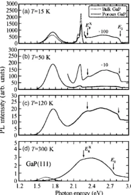
Figure 7 shows the PL spectra for the anodically etched GaP共111兲A sample in the HF:H2O2: C2H5OH = 1 : 1 : 2 elec-trolyte for t = 60 min at a constant current of 20 mA/ cm2.
They were obtained at T = 15– 300 K. For comparison, the PL spectra for the clean, bulk GaP sample obtained at T = 15 and 300 K are shown by the dashed lines in Figs. 7共a兲 and 7共d兲, respectively. The vertical arrows in Figs. 7共a兲–7共d兲 indicate the positions of the lowest-indirect-band-gap 共Eg
X兲
and lowest-direct-band-gap energies共E0兲.37,38
Similar to the case of the bulk GaP共100兲 sample 共Fig. 6兲, the PL spectrum for the bulk GaP 共111兲A sample mea-sured at T = 300 K shows a broad emission band at ⬃1.65 eV, originating from the molecular complexes ZnGa– OPand/or CdGa– OP, and an additional sharp peak near the Eg
X
edge of GaP at T⬍100 K. It is also seen that, in direct contrast to the PL emission from the porous GaP 共100兲 sample shown in Fig. 6, the GaP 共111兲A sample at T = 300 K shows a strong PL emission in the opaque region, i.e., at energies above⬃1.8 eV but below E0关see Fig. 7共d兲兴. Note that the PL intensity of the porous GaP共111兲A sample measured at T = 300 K is much stronger than that of the bulk sample.
At T = 15 K, no clear difference can be found in the transparent region 共E⬍Eg
X兲 of the PL spectra between the
porous and bulk GaP共111兲A samples 关Fig. 7共a兲兴. However, a markedly large difference can be found in the opaque region of the PL spectra between these two samples. Although the relative strength is approximately two orders smaller in the opaque region than in the transparent region, the supra-Eg X
component can be clearly detected on the porous GaP共111兲A sample, but not on the bulk sample. Note that the PL emis-sions in Fig. 7 are readily visible to the naked eye in 共a兲 green,共b兲 red, 共c兲 blue, and 共d兲 blue green.
FIG. 6. PL spectra for GaP 共100兲 sample anodically etched in HF : H2O2: C2H5OH = 1 : 1 : 2 electrolyte for t = 60 min at constant current of
20 mA/ cm2. The experimental data are taken at T = 15 and 300 K. For
com-parison, the PL spectra for clean, bulk GaP are shown by dashed lines. The vertical arrows indicate the positions of the lowest-indirect-band-gap energy
Eg X.37,38
FIG. 7. PL spectra for GaP 共111兲A sample anodically etched in HF : H2O2: C2H5OH = 1 : 1 : 2 electrolyte for t = 60 min at constant current of
20 mA/ cm2. The experimental data are taken at T = 14− 300 K. For
com-parison, the PL spectra for clean, bulk GaP are shown by dashed lines. The vertical arrows indicate the positions of the lowest-indirect-band-gap共Eg
X兲 and lowest-direct-band-gap energies共E0兲.37,38
Figure 8 shows a plot of the peak energy and height of the supra-Eg
X
component versus temperature T for the porous GaP共111兲A sample. The temperature variations of Eg
X
and E0 are also plotted in Fig. 8共a兲 as dashed and solid lines, respec-tively. These data were taken from Refs. 37 and 38. The supra-Eg
X emission plotted in Fig. 8共a兲 has its peak energy
falling in the range between Eg X
and E0. It is also found that the emission intensity exhibits a maximum at T⬃110 K 关Fig. 8共b兲兴.
Finally, we schematically show in Fig. 9 the energy-band structure and density-of-states spectrum N共E兲 for GaP. GaP is an indirect-band-gap semiconductor possessing the zinc-blende structure. The III-V semiconductor material GaP is suitable to study some of the indirect-band-gap effects, since it has three indirect band gaps, ⌫8共⌫15兲→X6共X1兲 near 2.26 eV, ⌫8共⌫15兲→X7共X3兲 near 2.48 eV, and ⌫8共⌫15兲 →L6共L1兲 near 2.63 eV, as well as the lowest-direct-band-gap ⌫8共⌫15兲→⌫6共⌫1兲 near 2.74 eV, at 300 K.21,38 The conduction-band 共CB兲 and valence-band 共VB兲 densities of states shown in Fig. 9共b兲 are represented by the well-known expressions of NC⬀共E−EC兲1/2 and NV⬀共EV− E兲1/2,
respec-tively.
From the deep-level transient spectroscopy and optically detected magnetic resonance in n-GaP,39,40the broad emis-sion band peaking at⬃1.7 eV has been recently attributed to the radiative recombination of nonequilibrium carriers via donor-acceptor共DA兲 pairs, the donor being a shallow center. The spectrum dominated near the indirect-band edge of ⬃2.2 eV at T=15 K can be assigned to the DA-pair recom-bination at sulfur-carbon pairs in bulk GaP and is well known from the literature.26–28The DA-pair emissions may be mainly emitted from the surrounding bulk GaP region.
The Eg X
-edge emission has been clearly observed only in the porous GaP共111兲A sample as a peak in the experimental PL spectrum at T = 40– 140 K 关see Figs. 7共b兲 and 7共c兲兴. In view of the experience gained in the study of the lumines-cence properties of porous silicon, it would be possible to consider that our observed supra-Eg
X
emission is the result of quantum size effects in the GaP nanocrystals produced dur-ing porous formation. Indeed, an emission peak in the UV spectral region 共⬎3 eV兲 has ever been observed on porous GaP and has been attributed to the quantum confinement of charged carriers in nanocrystalline GaP.5,6 Meijerink et al.7 have also observed UV emission in porous GaP but con-cluded that the emission is due to gallium oxide on the sur-face of the porous material.
The indirect optical transition process at the indirect-band edge can be expressed as a second-order time-dependent perturbation theory, while that at the direct-band edge is a first-order process.22 The higher-order process in the indirect-band edge is caused by the requirement of the momentum conservation with emitting and/or absorbing phonons. The indirect optical transition is, therefore, much weaker than the direct one. We consider here that our ob-served supra-Eg
X
emission is due to a nanostructure-induced relaxation of the momentum conservation in the porous GaP layer. The absence of long-range order in an amorphous ma-terial renders the Bloch theorem inapplicable and leaves the crystalline momentum បk undefined. The optical transition in such a case can be described, to a first approximation, by the nondirect or, in other words, quasidirect transition model in which conservation of the energy but not wave vector is significant.22,41 Note that the absence of k space in amor-phous materials does not imply that the density of electronic states is not a meaningful concept. The resultant nondirect transition model provides a single, broad absorption peak in optical spectra, which is typically observed in amorphous materials.21,42The nanostructured effect considered here is, thus, mainly to enable nondirect optical transition via relax-ation of the momentum conservrelax-ation, rather than enlarging the band gap of the porous GaP layer. In fact, our measured SE spectra do not clearly show the upshift of the band gap in the GaP nanostructures 共Fig. 5兲. The superlattice 共SL兲 is a typical example of a low-dimensional semiconductor mate-rial. In GaP / AlP and Si/ Ge SLs, the required k vector can be supplied from the superlattice itself due to the zone-folding effect, and the optical transition occurs without the aid of phonon emission and absorption.
The supra-Eg X
emission observed in Fig. 7 exhibits a steep high-energy end at the E0edge. This may be due to the absorption of the emitted light in the surrounding bulk GaP FIG. 8. 共a兲 Peak energy and 共b兲 peak height of supra-Eg
X
components vs temperature T for porous GaP 共111兲A sample anodically etched in HF : H2O2: C2H5OH = 1 : 1 : 2 electrolyte for t = 60 min at constant current of
20 mA/ cm2. The temperature variations of E
g X
and E0are also plotted in共a兲
by the dashed and solid lines, respectively.37,38
FIG. 9. 共a兲 Schematic energy-band structure and 共b兲 density-of-states spec-trum N共E兲 for GaP. The PL transitions are shown by the vertical arrows. The optical-absorption spectrum␣共E兲 for crystalline GaP is also plotted in 共c兲.21
region. As plotted in Fig. 9共c兲, the absorption coefficients are
␣⬃20 cm−1 at E⬃E g
X共⬃2.26 eV兲, ␣⬃1⫻104cm−1 at E ⬃E0共⬃2.74 eV兲, and gradually increases with increasing E, reaching a peak value ␣⬃2⫻106cm−1, at E ⬃E2共⬃5.3 eV兲.
21
The light penetration depth ␣−1 thus de-creases markedly from 500m at E⬃EgX, to 1m at E ⬃E0, and to 50 Å at E⬃E2. Photons with small diffusive penetration depths for E⬎E0can be detected only if they are emitted in the direction of the detector.43 Photons with very large diffusive penetration depths for E⬍Eg
X
can eventually reach the detector after being internally reflected inside the crystal or at the back surface of the crystal.
No supra-Eg X
luminescence has been observed on the po-rous GaP共100兲 sample 共Fig. 6兲. Note that the porous GaP 共100兲 sample has a thin crystalline-GaP surface layer with pits in every spot. The thickness of this layer is approxi-mately 0.5m 共Fig. 2兲. Therefore, photons with very large diffusive penetration depths, if they are emitted in the inner porous GaP region, would be strongly absorbed by this sur-face layer. As a result, only the infra-Eg
X
emission, but not the supra-Eg
X
emission, has been observed from the porous GaP 共100兲 sample 共Fig. 6兲.
IV. CONCLUSIONS
We studied the structural and optical properties of po-rous GaP using SEM, SE, and PL spectroscopy. The popo-rous GaP structures were fabricated by electrochemical etching on 共100兲-oriented and 共111兲A-oriented n-GaP substrates in an aqueous electrolyte of HF : H2O : C2H5OH = 1 : 1 : 2. The SEM images suggested that the morphology of the porous surface is strongly dependent on the substrate orientation. At the be-ginning of the GaP共100兲 process, etching started to form pits in the direction vertical to the sample. After initial pitting, further etching proceeded in all directions radially away from the initial etch pit. The GaP 共100兲 surface finally showed a cellular structure with the etch pit as a nucleus, but no further roughening occurred on the surface region.
The pore morphology developed on the GaP共111兲A sur-face was quite different from that observed on the GaP共100兲 surface. No pitting was observed at the beginning of the anodization on the共111兲A surface. Further anodization led to a共111兲A surface with a pillar structure characterized by an array of petal-like patterns; each petal-like pattern consists of a lot of columns growing radically and stretching parallel to the 共111兲A surface, resulting in microscopic roughening of the surface. Prolonged anodization led to the formation of a beehivelike porous network inside the sample.
The PL spectra for the porous GaP共100兲 sample showed only the red emission band at⬃1.65 eV at 300 K and the red emission band at⬃1.75 eV together with the DA-pair emis-sion at ⬃2.2 eV at low temperatures. The red and DA-pair emission bands have been typically observed in bulk GaP. Apart from the red emission band, the supra-Eg
X
emission has been clearly observed on the porous GaP共111兲A sample at all temperatures studied 共T=15–300 K兲. The observed supra-Eg
X
emission exhibited the steep high-energy end at the
E0 edge. This emission is considered to be due to a nanostructure-induced relaxation of momentum conservation in the porous GaP layer.
1L. T. Canham, Appl. Phys. Lett. 57, 1046共1990兲.
2A. G. Cullis, L. T. Canham, and P. D. J. Calcott, J. Appl. Phys. 82, 909
共1997兲.
3L. Canham, Properties of Porous Silicon共INSPEC, London, 1997兲. 4S. Ossicini, L. Pavesi, and F. Priolo, Light Emitting Silicon for
Micropho-tonics共Springer, Berlin, 2003兲.
5A. Anedda, A. Serpi, V. A. Karavanskii, I. M. Tiginyanu, and V. M.
Ichizli, Appl. Phys. Lett. 67, 3316共1995兲.
6K. Kuriyama, K. Ushiyama, K. Ohbora, Y. Miyamoto, and S. Kakeda,
Phys. Rev. B 58, 1103共1998兲.
7A. Meijerink, A. A. Bol, and J. J. Kelly, Appl. Phys. Lett. 69, 2801
共1996兲.
8P. Schmuki, D. J. Lockwood, H. J. Labbè, and J. W. Fraser, Appl. Phys.
Lett. 69, 1620共1996兲.
9P. Schmuki, L. E. Erickson, D. J. Lockwood, J. W. Fraser, G. Champion,
and H. J. Labbè, Appl. Phys. Lett. 72, 1039共1998兲.
10P. Schmuki, L. Santinacci, T. Djenizian, and D. J. Lockwood, Phys. Status
Solidi A 182, 51共2000兲.
11G. Su, Q. Guo, and R. E. Palmer, J. Appl. Phys. 94, 7598共2003兲. 12U. Schlierf, D. J. Lockwood, M. J. Graham, and P. Schmuki, Electrochim.
Acta 49, 1743共2004兲.
13V. Ichizli, H. L. Hatnagel, H. Mimura, H. Shimawaki, and K. Yokoo,
Appl. Phys. Lett. 79, 4016共2001兲.
14V. N. Tondare, M. Naddaf, A. B. Bhise, S. V. Bhoraskar, D. S. Joag, A. B.
Mandale, and S. R. Sainkar, Appl. Phys. Lett. 80, 1085共2002兲.
15I. M. Tiginyanu, I. V. Kravetsky, S. Langa, G. Marowsky, J. Monecke, and
H. Föll, Phys. Status Solidi A 197, 549共2003兲.
16M. Christophersen, J. Carstensen, S. Rönnebeck, C. Jäger, W. Jäger, and
H. Föll, J. Electrochem. Soc. 148, E267共2001兲.
17B. H. Erné, D. Vanmaekelbergh, and J. J. Kelly, J. Electrochem. Soc. 143,
305共1996兲.
18R. W. Tjerkstra, J. Gómez Rivas, D. Vanmaekelbergh, and J. J. Kelly,
Electrochem. Solid-State Lett. 5, G32共2002兲.
19T. Smith, J. Opt. Soc. Am. 58, 1069共1968兲.
20S. Anderieu and F. A. d’Avitaya, Surf. Sci. 219, 277共1989兲.
21S. Adachi, Optical Constants of Crystalline and Amorphous
Semiconduc-tors: Numerical Data and Graphical Information共Kluwer Academic,
Bos-ton, 1999兲.
22S. Adachi, Optical Properties of Crystalline and Amorphous
Semiconduc-tors: Materials and Fundamental Principles共Kluwer Academic, Boston,
1999兲.
23D. E. Aspnes, J. B. Theeten, and F. Hottier, Phys. Rev. B 20, 3292共1979兲. 24R. M. A. Azzam and N. M. Bashara, Ellipsometry and Polarized Light
共North-Holland, Amsterdam, 1977兲.
25K. Sakaino and S. Adachi, J. Electrochem. Soc. 149, G543共2002兲. 26A. N. Pikhtin and O. L. Lazarenkova, in Handbook of Electroluminescent
Materials, edited by D. R. Vij共Institute of Physics Publishing, Bristol,
2004兲, p. 282.
27P. J. Dean, C. J. Frosch, and C. H. Henry, J. Appl. Phys. 39, 5631共1968兲. 28P. J. Dean, J. D. Cuthbert, and R. T. Lynch, Phys. Rev. 179, 754共1969兲. 29A. I. Belogorokhov, V. A. Karavanski
, A. N. Obraztsov, and V. Y. Ti-moshenko, JETP Lett. 60, 274共1994兲.
30A. V. Zoteev, P. K. Kashkarov, A. N. Obraztsov, and V. Y. Timoshenko,
Semiconductors 30, 775共1996兲.
31A. A. Lebedev, V. Y. Rud’, and Y. V. Rud’, Tech. Phys. Lett. 22, 754
共1996兲.
32M. A. Stevens-Kalceff, I. M. Tiginyanu, S. Langa, H. Föll, and H. L.
Hartnagel, J. Appl. Phys. 89, 2560共2001兲.
33M. A. Stevens-Kalceff, S. Langa, I. M. Tiginyanu, J. Carstensen, M.
Christophersen, and H. Föll, Mater. Res. Soc. Symp. Proc. 638, F5.31.1 共2001兲.
34T. Takizawa, S. Arai, and M. Nakahara, Jpn. J. Appl. Phys., Part 2 33,
L643共1994兲.
35A. Liu and C. Duan, Appl. Phys. Lett. 78, 43共2001兲.
36I. M. Tiginyanu, E. Monaico, V. V. Ursaki, V. E. Tezlevan, and R. W.
Boyd, Appl. Phys. Lett. 86, 063115共2005兲.
37S. Adachi, Properties of Group-IV, III–V and II–VI Semiconductors
共Wiley, Chichester, 2005兲.
Compound Semiconductors共Kluwer Academic, Boston, 2004兲 Vol. 2.
39Y. Ishikawa, Y. Hayashi, and N. Itoh, J. Appl. Phys. 65, 2035共1989兲. 40O. O. Awadelkarim, M. Godlewski, and B. Monemar, Mater. Sci. Forum
38–41, 821共1989兲.
41D. T. Pierce and W. E. Spicer, Phys. Rev. B 5, 3017共1972兲.
42J. Tauc, in Amorphous and Liquid Semiconductors, edited by J. Tauc
共Ple-num, London, 1974兲, p. 159.
43A. F. van Driel, B. P. J. Bret, D. Vanmaekelbergh, and J. J. Kelly, Surf.
Sci. 529, 197共2003兲.