INVITED PAPER
Special Section on Microwave PhotonicsGenerating UWB and Microwave Waveforms Using Silicon Photonics
Lawrence R. CHEN†a),Nonmember
SUMMARY We provide an overview of techniques for the photonic generation of arbitrary RF waveforms, particularly those suitable for im- pulse radio or multi-band ultrawideband (UWB)-over-fiber transmission, and chirped microwave waveforms, with an emphasis on microwave pho- tonic filtering and optical spectral shaping followed by wavelength-to-time mapping. We discuss possibilities for integrating the various device and component technologies with silicon photonics.
key words: microwave photonics, silicon photonics, waveform generation
1. Introduction
Techniques for generating arbitrary RF waveforms are im- portant for a broad range of applications from communica- tions to imaging and sensing to instrumentation. For exam- ple, ultrawideband (UWB) has attracted interest for short- range, high-speed wireless communications and sensor net- works. The use of UWB-over-fiber has recently emerged as a viable approach to extend reach and the area covered[1].
In this sense, in addition to being primed for optical trans- mission, photonic generation of UWB signals can exploit the optical components and technologies that are already in- volved. Photonic approaches also provide increased flexi- bility, particularly with regards to reconfigurability and tun- ability. This is extremely valuable for generating waveforms that are suitable for impulse radio (IR) UWB, e.g., doublets or triplets, as well as multi-band (MB) UWB where the elec- trical spectrum is separated into multiple channels with cor- respondingly longer waveforms in the time domain. Finally, photonic approaches may enable different modulation for- mats, including pulse polarity modulation, pulse shape mod- ulation, and bi-phase modulation.
As a second example, chirped microwave waveforms (and their subsequent compression) are useful in radar sys- tems for increasing detection distance or resolution[2].
While such waveforms can be generated in the electronic domain, their bandwidths and central frequencies are lim- ited by the sampling rate of digital electronics. On the other hand, photonic techniques offer the possibility of achieving central frequencies of tens to hundreds of GHz as well as significant chirp rates, thereby supporting tens of GHz of bandwidth. As with UWB generation, the use of photonics also offers the possibility for tuning and reconfiguration, as
Manuscript received January 15, 2015.
Manuscript revised March 6, 2015.
†The author is with the Department of Electrical and Computer Engineering, McGill University, Montreal, QC H3A 0E9 Canada.
a) E-mail: [email protected] DOI: 10.1587/transele.E98.C.752
well as compatibility with fiber optic transmission.
A variety of techniques for photonic generation of IR- UWB, MB-UWB, and chirped microwave waveforms have been reported. These include, amongst others, the use of optical frequency combs, nonlinear optical effects in fiber or semiconductor optical amplifiers, phase modulation-to- intensity modulation using discrimination filters, optical spectral shaping followed by wavelength-to-time mapping, direct space-to-time pulse shaping, temporal pulse shaping, and microwave photonic filters (MPFs)[3],[4].
Typically, the system implementations are based on discrete components and involve bulky (e.g., fiber-based) and/or benchtop components. In recent years, there has been a focus on integration, particularly to address issues related to compactness, stability, power consumption, and ultimately mass production for reduced cost and practical deployment[5]. In this paper, we describe the use of silicon photonics (SiP) for generating UWB and chirped microwave waveforms. SiP is emerging as the platform of choice over other semiconductor technologies such as InP for photonic integration. In addition to providing a small footprint, the ability to integrate active with passive devices, and the pos- sibility to reduce power consumption, SiP uses the same processing tools as CMOS fabrication. This has resulted in high quality control, increased yield (reliability), as well as performance of SiP integrated circuits thereby paving the pathway for commercialization[6],[7]. In this paper, we consider the implementation of MPFs and optical spectral shapers in SiP.
The remainder of this paper is organized as follows.
Section 2 describes MPFs for generating RF waveforms, e.g., for IR-UWB and MB-UWB transmission. Section 3 reviews optical spectral shaping followed by wavelength-to- time mapping for generating chirped microwave waveforms.
Finally, perspectives and conclusions are given in Sect. 4.
2. Generating UWB and RF Waveforms Using Mi- crowave Photonic Filters
In this section, we discuss the use of MPFs to generate UWB and RF waveforms. After illustrating the basic principle of waveform generation, we provide a brief review of MPFs.
Next, we describe specific examples of generating IR-UWB and MB-UWB waveforms with MPFs. We then present an approach for generating arbitrary waveforms based on an MPF involving nonlinear mixing in a silicon nanowire (SNW). This is followed by a discussion of implementing Copyright c2015 The Institute of Electronics, Information and Communication Engineers
Fig. 1 (a) Concept of Fourier transform optical pulse shaping with opti- cal filters and (b) RF waveform generation based on MPFs.
MPF building blocks in SiP.
2.1 Basic Principle
Figure 1 (a) shows the general schematic for optical pulse shaping based on using an optical filter to tailor the ampli- tude and phase of the spectral content associated with an ul- trashort optical input pulse (also referred to as Fourier trans- form optical pulse shaping)[8]. The transfer function (spec- tral response) of the optical filter,Hopt(ω), must satisfy the relationship
Hopt(ω)=|Hopt(ω)|exp(jφHopt(ω))=Eoptout(ω)
Eoptin (ω) (1) where Eoutopt(ω) and Einopt(ω) are the Fourier transforms of the output and input electric fields, respectively, of the de- sired optical waveform and input ultrashort optical pulse.
Assuming that the synthesized output waveform is longer in duration than the input (which is typical in most opti- cal pulse shaping applications), the spectrum of the output signal is given approximately by that of the filter response, Eoptout(ω) ≈Hopt(ω), i.e., the filter operates over a relatively flat (constant) portion of the input spectrum. In an analogous manner, as depicted in Fig. 1 (b), a microwave filter with fre- quency response HRF(Ω) can be used to process an input RF impulse represented by its Fourier transform, ERFin (Ω), according to
EoutRF(Ω)=HRF(Ω)ERFin (Ω) (2) where EoutRF(Ω) is the Fourier transform of the desired out- put waveform (we have usedΩto denote frequencies in the microwave range to distinguish them fromω, which repre- sents optical frequencies). Again, if the synthesized output waveform is long in duration compared to the input, then ERFout(Ω) ≈ HRF(Ω). In this paper, we consider the use of MPFs to realize the desired microwave filter responses.
2.2 Brief Review of Microwave Photonic Filters
The field of MPFs is extremely rich and the design of filters
Fig. 2 General schematic of an MPF.
with reconfiguration and/or tuning capabilities has been the subject of intense research. Indeed, many filter structures have been proposed, including those with notch responses, tailored responses involving complex tap coefficients, dis- persive filters or those with specific phase profiles, and sin- gle or multiple passband responses. Excellent review arti- cles on MPFs and microwave photonic signal processing can be found in[9]–[12]. For completeness, we provide some of their salient features.
The typical MPF structure is illustrated in Fig. 2. The input microwave signal xin(t) is converted to the optical domain via modulation (E/O conversion), e.g., using an electro-optic modulator (EOM) fed by a single carrier fre- quency or multiple carrier frequencies source. The electric field of the modulated optical signal, ein(t), which carries the information about the input microwave signal, is then processed in the optical domain by a photonic subsystem.
The purpose of the subsystem is to take samples of the microwave signal, which are conveyed by the optical car- rier(s), and weigh, delay, and combine them. The subsys- tem can comprise a variety of components, from passive de- vices such as couplers, variable optical attenuators (VOAs), fiber Bragg gratings (FBGs), and fiber delay lines to active components such as Erbium-doped or semiconductor opti- cal amplifiers. After photonic processing, the power of the output optical signal, |eout(t)|2, is detected using an optical receiver (O/E conversion) to remove the optical carrier(s) and extract the processed microwave signalxout(t).
Generally speaking, the MPF cannot be viewed as a linear system relatingxin(t) andxout(t). However, under cer- tain conditions (see further[10]), we can consider a linear operation such that the input and output microwave signals are related by
xout(t)=xin(t)∗hRFMPF(t) (3) where hRFMPF(t) is the MPF impulse response with corre- sponding frequency responseHRFMPF(Ω). Note that the MPF frequency response does not correspond directly to the transfer function of the photonic subsystem. However, cer- tain features of the photonic subsystem are correlated to the MPF response. For example, if the photonic subsystem in- volves feedback, the MPF transfer function can take on the form of an infinite impulse response (IIR) filter; on the other
hand, it will have the form of a finite impulse response (FIR) filter when there is no optical feedback. In the discussion that follows, we restrict ourselves to FIR MPFs.
Consider an optical source comprising multiple carrier frequencies that are uniformly spaced, e.g., from a bank of lasers. Assuming incoherent superposition of the carriers (samples or taps), the MPF frequency response is given by
HRFMPF(Ω)∝ N
m=1
Pmexp[−j(m−1)ΩΔτ] (4) whereNis the number of taps,Pmis the amplitude (weight) of themthtap,Δλis the wavelength separation between taps, andΔτ=DΔλis the tap delay withDbeing the dispersion in [ps/nm] of the medium used to implement the delay. The tap amplitudes can be controlled to shape (reconfigure) the filter response while the tap delay can be varied to tune the frequency response. Note that the MPF frequency response is periodic with a period 2π/Δτ=2π/(DΔλ).
2.3 Review of Results Using Fiber-Based Implementa- tions
Figure 3 illustrates several different MPF implementations and the overall system for generating IR-UWB and MB- UWB waveforms[13]–[16]. The MPFs use multiple car- rier frequencies which are generated either with several dis- crete lasers as in Fig. 3 (a)[13]or by spectral slicing a broad- band source as in Figs. 3 (b) and (c)[14]–[16]. In Fig. 3 (b), an arrayed waveguide grating (AWG) is employed to cre- atediscretespectral slices; VOAs provide control over their amplitudes. A number of space switches and a second set of AWGs select and direct the spectral slices to one of two EOMs where E/O conversion occurs. The EOMs are biased for operation on opposite slopes of the modulator transfer function so as to obtain positive or negative taps. Note that a spectral slice can implement a positive tap or a negative tap, but not both at the same time. The MPF implementa- tion in Fig. 3 (a) is similar except that discrete lasers replace the broadband source and AWGs to define the taps (the tap amplitudes can be set by adjusting the powers of the lasers).
In all cases, a length of single mode fiber (SMF) is used as a dispersive medium to create the necessary tap delays.
The input to the MPF is a broadband RF signal, i.e., a short electrical pulse. The MPF response is then configured to shape the input RF spectrum to obtain the desired out- put temporal waveform as described by Eq. (2). Note that we can also interpret the system operation as generating a specific temporal waveform whose electrical spectrum sat- isfies a given requirement, e.g., for IR-UWB or MB-UWB transmission.
Figure 4 highlights examples of the different wave- forms that can be generated. For example, pulse doublets obtained using the MPFs in Figs. 3 (a) and (b) are shown in Figs. 4 (a) and (b), respectively. In both cases, 3 taps are employed with a weight distribution of [0.5,−1,0.5]. In Fig. 4 (a), the taps are based on 3 discrete lasers with a wave-
Fig. 3 General schematic of MPFs and systems for generating IR-UWB and MB-UWB waveforms. The MPFs are implemented with (a) discrete lasers (after[13]), (b) spectral slicing with AWGs (after[14],[15]), and (c) spectral slicing with a periodic optical filter and balanced detection (after [16]). BBS: broadband source, PC: polarization controller, ODL: optical delay line (all schematics are courtesy of and adapted from J. Mora).
length separation of 0.74 nm (centered at 1550.12 nm) and 5.43 km of SMF is used to provide a tap delay of∼68 ps. In Fig. 4 (b), the taps are based on 3 adjacent channels from an AWG with a 3 dB channel bandwidth of 0.4 nm and channel spacing of 0.8 nm (centered near 1547.72 nm);
again 5.43 km of SMF is used to provide the tap delay (∼74 ps). Note that the characteristics of the waveforms—in time and in electrical spectrum—are very similar regardless of whether discrete lasers or a spectrally sliced broadband source is used (the wavelength separation between taps and tap delay are approximately the same). By increasing the number of taps and controlling their amplitudes to create an apodized profile, a Gaussian-like waveform can be gener- ated, giving rise to a signal that is suitable for MB-UWB communications. The results obtained using the MPF in Fig. 3 (b) with a broadband source having a Gaussian-like spectrum and 3 dB bandwidth of 8 nm centered at∼1546 nm and 23 taps are depicted in Fig. 4 (c) [the AWG has the same characteristics as described above and 5 km of SMF is used to provide the tap delay].
The MPF shown in Fig. 3 (c) differs from those in Figs. 3 (a) and (b) in two regards. First, a periodic optical fil-
Fig. 4 Pulse doublet generated using (a) the MPF from Fig. 3 (a) (after [13]) and (b) the MPF from Fig. 3 (b) (after[14]). (c) A Gaussian-like waveform suitable for MB-UWB transmission generated using the MPF from Fig. 3 (b) (after[15]). The corresponding electrical spectra are also shown (all results are courtesy of and adapted from J. Mora).
ter, here based on a Mach-Zehnder delay line interferometer (MZ-DLI), is used for spectral slicing. In this case, the re- sultingsinusoidalandcontinuoustap distribution produces a single bandpass MPF[17]. Second, a balanced photodiode (BPD) is used for O/E conversion. This allows both positive and negative portions in the generated electrical temporal waveform and differential detection removes the DC com- ponent of the signal. To control the weight of the sinusoidal and continuous taps, the spectrum of the broadband source is first shaped with an optical filter. By tuning the delay in the MZ-DLI, the free spectral range (FSR) of the periodic optical filter can be tuned. For a fixed length of SMF, this causes the tap delay to vary, which in turn tunes the pass- band frequency of the MPF response. Figure 5 (a) shows the generation of Gaussian-like waveforms with different peri- ods; sample electrical spectra demonstrating tuning appear in Fig. 5 (b). These results were obtained using a broadband source with a Gaussian-spectrum and a 3 dB bandwidth of 16 nm centered at 1546.9 nm and using 5 km of SMF to set the tap delay; the delay in the MZ-DLI was tuned between
Fig. 5 (a) Gaussian-like temporal waveforms with different periods gen- erated using the MPF in Fig. 3 (c). (b) Sample electrical spectra (after[16]).
(All results are courtesy of and adapted from J. Mora).
2.9 ps and 7.2 ps.
We now describe an alternate implementation of a reconfigurable MPF for generating arbitrary RF wave- forms[18]. Figure 6 (a) illustrates a schematic of the pro- posed approach. As with the systems described previously, it is based on a FIR MPF. Partially degenerated four wave mixing (FWM) in a nonlinear medium is used to increase the number of optical carriers/taps[18]–[20]. In particular, at leastN=2Mtaps can be obtained starting fromMsources.
The tap weights are adjusted using a spectral shaper in order to control the MPF amplitude response and correspondingly, the generated RF waveform. As mentioned previously, ad- justing the tap delay Δτallows for tuning the central fre- quency of the MPF passband response. The taps are then split by a 3 dB coupler and the two copies are delayed rel- ative to each other by an additional amount ofΔτ/2 before being detected with a BPD.
Figure 6 (b) depicts the experimental setup where an SNW serves as the nonlinear medium. The SNW is 20 mm in length and has a cross-section of W ×H = 500 nm× 220 nm with a top oxide cladding. It is designed to have a small amount of anomalous dispersion near 1550 nm with a dispersion slope∼0 ps/(nm2·km) for broadband FWM[20].
Vertical grating couplers (VGCs) are used for input and out- put coupling and to ensure operation with TE-polarized light in the SNW. The total fiber-to-fiber coupling loss is∼22 dB and each VGC introduces∼10 dB insertion loss (recent de- signs can reduce this loss further to∼4 dB per coupler[21]).
To demonstrate the principle, we use M = 2 optical sources (at 1547 nm and 1550 nm). An electric impulse generator drives the EOM for O/E conversion (the modu- lated optical pulses have a FWHM duration of∼100 ps); the corresponding spectrum of the electric impulses is shown in the inset of Fig. 6 (b). The modulated optical taps are ampli- fied to an average power of∼14 dBm before being coupled into the SNW. After FWM in the SNW, the 4 output taps are
Fig. 6 (a) Schematic of the proposed RF arbitrary waveform generator based on anN-tap FIR MPF. (b) Corresponding experimental setup. The inset shows the RF spectrum of the electrical pulses. CW: continuous wave, Disp: dispersive medium, TLS: tunable laser source, DFB: distributed feed- back laser, CSA: communications signal analyzer, RF-SA: radio-frequency spectrum analyzer.
amplified and their amplitudes are controlled using a bench- top spectral shaper (Finisar Waveshaper 1000-S, WS). They are amplified again before propagating through∼5 km of SMF to provide a tap delay ofΔτ = 250 ps. The taps are split equally into 2 copies with a 3 dB coupler and their rel- ative delay is set toΔτ/2 =125 ps using a pair of tunable optical delay lines (ODLs). The two copies are detected us- ing a 45 GHz BPD.
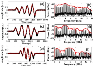
Figures 7 (a)–(c) show the optical spectrum at the out- put of the EOM (before the SNW), after FWM in the SNW to increase the number of taps, and after the spectral shaper set to provide equal weight taps. The correspond- ing temporal waveform and electrical spectrum are shown in Figs. 7 (d) and (e). The RF spectrum, centered at 3.98 GHz, has a shape that is expected for an MPF comprising uniform taps and for a waveform with a constant envelope.
Figure 8 illustrates the capability of the approach to generate different waveforms and to tune the central fre- quency. For example, Fig. 8 shows the waveforms and cor- responding electrical spectra when the spectral shaper con- trols the tap weights to obtain sawtooth and apodized pro- files. For the apodized waveform, there is a clear reduction
Fig. 7 Results for a uniform waveform with 4 taps. Optical spectrum at (a) the output of the EOM (before the SNW), (b) after FWM in the SNW, (c) after the spectral shaper; (d) corresponding temporal waveform, and (e) electrical spectrum. Measurements (dotted, black) and simulations (solid, red).
Fig. 8 Results for a sawtooth waveform with 4 taps: (a) temporal wave- form and (b) RF spectrum. Results for an apodized waveform with 4 taps:
(c, e) temporal waveforms and (d, f) RF spectra. Δτ=250 ps (c, d) and Δτ=180 ps (e, f). Measurements (dotted, black) and simulations (solid, red).
in the sidelobe level as compared with Fig. 7 (e). By reduc- ing the tap delay toΔτ = 180 ps, we can tune the central frequency of the MPF passband, see Fig. 8 (e) [note that the ODLs need to be re-adjusted to provide a relative delay of Δτ/2=90 ps between the two copies]. While the temporal waveform exhibits a ‘skew’ due to the fact that the pulses corresponding to the taps overlap slightly in time, i.e., the separation between a positive and negative pulse is 90 ps whereas the duration of each pulse is 100 ps, the RF spec- trum shifts to 5.49 GHz and exhibits a similar shape to that in Fig. 8 (d). Tuning of the apodized waveforms can be use- ful for MB-UWB communications.
In all of the results shown above, shorter electrical pulses at the input to the system (equivalently with a broader input spectrum) will allow for a greater range of waveforms to be synthesized (including at higher frequencies). More- over, increasing the number of taps will provide greater con- trol over the MPF filter response, and hence the generated waveforms. The results also correspond to MPFs that have a linear phase response. MPFs can be designed with non-
linear phase responses[22]–[24]; in this case, we can cre- ate chirped waveforms or perform pulse compression. This provides yet another degree of freedom for waveform gen- eration.
2.4 Towards an Integrated Solution
While the MPFs described in Sect. 2.3 involve discrete fiber and/or benchtop components, a number of these building blocks or their functionalities have been realized in SiP.
First, in-line SNW VOAs with a dynamic range of 30 dB and capable of operating at speeds of up to 1 GHz[25]as well as SiP space switches integrated with CMOS drivers have been demonstrated[26]. Next, a 512×512 AWG router with 25 GHz channel spacing was recently reported[27].
O/E and E/O conversion with SiP technologies can be read- ily achieved: a number of high-performance SiP modulators exist[28], including those capable of advanced modulation formats[29], as well as PDs and BPDs[30],[31].
Various forms of optical delays in silicon have also been demonstrated. These include delay lines based on pho- tonic crystals, coupled ring resonators, and various Bragg- grating structures such as serial grating arrays, step-chirped gratings, continuously chirped gratings, and cascaded grat- ings. With grating structures, delays up to several hundreds of ps spanning a few nm or tens of ps spanning broader wavelength ranges are readily accessible[19],[32]–[34].
In addition to realizing discrete building blocks in SiP, there have been significant efforts at integrating various de- vices to increase processing capability and functionality.
For example, AWG routers, modulators, and photodiodes have been integrated to implement an 8×8 SiP optical switch for high performance computing and data center applica- tions[35]. The ability to integrate various building blocks will allow for the realization of compact, high performance MPFs for generating arbitrary RF waveforms for a variety of applications. Indeed, there have been recent demonstrations of integrated MPFs in various material platforms[5],[36]–
[39].
3. Generating Chirped Microwave Waveforms Based on Optical Spectral Shaping and Wavelength-to- Time Mapping
In this section, we describe the generation of chirped mi- crowave waveforms based on optical spectra shaping fol- lowed by wavelength-to-time mapping[4],[40]–[42]. We begin with a brief review of the relevant theory, followed by an overview of recently demonstrated results based on fiber implementations. We then discuss progress in developing integrated spectral shapers in SiP.
3.1 Principle of Operation
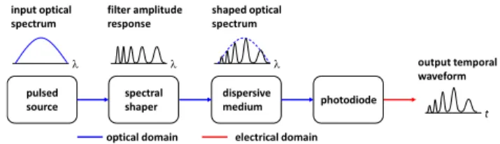
A schematic of the principle of operation is shown in Fig. 9.
The system comprises a broadband source, e.g., from a mode-locked fiber laser, an optical pulse/spectral shaper,
Fig. 9 General system for generating chirped microwave waveforms based on optical spectral shaping followed by wavelength-to-time mapping.
and a dispersive medium. The spectral shaper is used to modify the spectrum of the pulsed source, typically in am- plitude only. The shaped spectrum then propagates through the dispersive medium where a wavelength-to-time mapping process takes place, i.e., the shape of the spectrum is mapped to the time domain. The resulting temporal signal corre- sponds to the microwave waveform which is detected by a PD. Note that the linearity of the system allows for the or- der of spectral shaping and wavelength-to-time mapping to be interchanged. The key component in the system is the spectral shaper: it must be capable of generating the desired amplitude spectrum which ultimately corresponds to the de- sired microwave waveform.
Wavelength-to-time mapping is based on real-time Fourier transformation of an input signal in a dispersive medium[43]. For example, consider a dispersive medium where the relative delay and frequency are related linearly byt =Φω¨ where ¨Φis the first-order dispersion coefficient ( ¨Φ = d2Φ/dω2 withΦ being the phase of the dispersive medium). Leta(t) be an input signal with pulse durationΔt0 to the dispersive medium. The output signalb(t) is given by [43]:
b(t)∝A(ω)ω=t/Φ¨ (5)
where A(ω) is the Fourier transform ofa(t) when Δ2 ¨Φt20 π (the input signal must be confined within a time window that satisfies this condition). The main point of Eq. (5) is that the envelope of the output signal b(t) in time corresponds to the spectrum of the input signala(t). The linear relation- shipt = Φω¨ sets a linear wavelength-to-time mapping. It is also possible to consider a nonlinear wavelength-to-time mapping, e.g., with a higher-order dispersive medium. In particular, if the relative delay can be represented as
t=Φω¨ +1 2
...Φω2 (6)
where...
Φ(=d3Φ/dω3) is the second-order dispersion coeffi- cient, we obtain the following nonlinear wavelength-to-time mapping[44]:
ω=−Φ¨ ±
Φ¨2+2...
Φt
...Φ (7)
To generate a uniform (sinusoidal-like) microwave waveform, we require a spectral shaper with a sinu- soidal/periodic filter response, i.e., with uniform (constant) FSR, followed by a linear wavelength-to-time mapping. To
generate a chirped microwave waveform, there are two ap- proaches: the first uses a spectral shaper with a periodic response followed by a nonlinear wavelength-to-time map- ping[44],[45]while the second uses a spectral shaper with an aperiodic response followed by a linear wavelength-to- time mapping[46],[47]. Generally speaking, by control- ling the FSR (or variation in FSR), as well as the first-order and/or second-order dispersion coefficients, we can tailor the central frequency and chirp rate of the generated mi- crowave waveforms.
3.2 Review of Results Using Fiber-Based Implementa- tions
It is relatively simple to realize (all-fiber) sinusoidal/periodic optical filters. For example, we can use a fiber-based MZ- DLI or incorporate a short length of polarization maintain- ing fiber (PMF) in a Sagnac loop. In these cases, the FSR of the filters are determined by the delay in the MZ-DLI or length of PMF in the Sagnac loop.
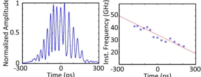
To obtain a nonlinear wavelength-to-time mapping, a nonlinearly chirped FBG can be used as the dispersive medium. A number of well-established approaches exist to produce FBGs with tailored dispersive properties (in large part due to the development of FBG-based dispersion com- pensating modules for fiber optic communications): a non- linear chirped phase mask can be employed or a linear strain or temperature gradient can be applied to a linearly chirped FBG. The latter approach was exploited in[44]to realize a tunable nonlinearly chirped FBG spanning a bandwidth of∼12 nm (e.g., with first- and second-order dispersion co- efficients of ¨Φ = 295.1 ps2 and ...
Φ = 20.9 ps3). By us- ing a spectral shaper based on a length of PMF in a Sagnac loop (to generate a uniform comb of slices from broadband pulses with a 3 dB bandwidth of 8 nm), chirped microwave waveforms 243 ps in duration with an instantaneous fre- quency varying from 25 GHz to 43 GHz, corresponding to a chirp rate of 0.074 GHz/ps, were obtained[44](see Fig. 10).
While the overall system is simple to implement, the use of FBGs to implement a nonlinear wavelength-to-time map- ping causes several issues. First, long gratings, e.g., several cm’s to 1 m, are required to have both broad bandwidth and large dispersion. Moreover, the group delay ripple needs to be minimized to avoid degradation in the chirped microwave
Fig. 10 Pulse profile and instantaneous frequency vs. time for chirped microwave waveforms generated using a periodic spectral filter and a non- linearly chirped FBG (adapted from and courtesy of J. Yao).
waveforms, especially if they are to be compressed subse- quently.
The use of a spectral shaper with an aperiodic response followed by a linear wavelength-to-time mapping, e.g., in a length of SMF or dispersion compensating fiber, avoids the problems associated with nonlinearly chirped FBGs (al- beit at the expense of compactness). Although more com- plex in design, aperiodic optical filters can nonetheless be implemented readily using FBGs or ring resonators in SiP.
A simple all-fiber distributed Fabry-P´erot (FP) filter can be formed by superimposing two spatially offset and linearly chirped FBGs as shown in Fig. 11[48]. If the FBGs have different chirp rates, the FSR becomes wavelength depen- dent[46]:
FS R(λ)= λ20 2neff
L+CC11−CC22(λ−λ0) (8) whereneff is the effective index of the fiber,C1 andC2 are the chirp rates, Lis the spatial offset between the gratings, andλ0is the starting wavelength. To simplify fabrication, it is possible to use two identical linearly chirped FBGs with opposite orientation (C1=−C2).
To demonstrate the principle, two 1 cm long linearly chirped FBGs were employed to realize a spectral shaper spanning a wavelength range of ∼1.5 nm with variable FSR. The spectral shaper was used to shape the spectrum of broadband pulses from a mode-locked fiber laser (3 dB bandwidth of 8 nm); with 58 km of SMF as the dispersive medium, chirped microwave waveforms 1,250 ps in dura- tion with a central frequency of 15 GHz and a chirp rate of 0.022 GHz/ps were synthesized[46]. The results are sum- marized in Fig. 12.
Once the grating parameters are set, it is not possible to vary the FSR of the spectral shaper and as such, it is not possible to tune the chirped microwave waveform. To overcome this limitation, a spectral shaper based on incor- porating a linearly chirped FBG within a Sagnac loop was proposed[47], see Fig. 13.
The transfer function (response) of a Sagnac loop in- corporating an FBG can be written as[49]:
T = |Eout|2
|Ein|2 =Rg(λ) cos 2πneff
λ ΔL+φ(λ)−φ(λ) 2
(9)
Fig. 11 Schematic of an all-fiber distributed FP resonator with varying FSR based on two superimposed and spatially offset linearly chirped FBGs.
Fig. 12 (a) Spectral response of all-fiber distributed FP resonator with increasing FSR. (b) Pulse profile and instantaneous frequency of the gener- ated microwave waveform with negative chirp (courtesy of J. Yao).
Fig. 13 An all-fiber spectral shaper based on a Sagnac loop incorporating a linearly chirped FBG. PC: polarization controller.
whereRg(λ) is the reflectivity of the grating,φ(λ) andφ(λ) are the phase delays in reflection for light entering clock- wise and counter-clockwise, respectively, andΔL=L1−L2
is the path mismatch in the loop. For a uniform FBG, φ(λ) =φ(λ) and for equal path lengths,ΔL = 0 such that the transfer function corresponds to the FBG reflection re- sponse: T = Rg(λ). For a uniform grating withΔL 0, the grating response is modulated sinusoidally, yielding a periodic or comb-like filter. When the grating is nonuni- form,φ(λ)φ(λ). For a linearly chirped FBG with a linear chirp rateC(nm/cm), we can re-write the transfer function in Eq. (9) as:
T =1 2Rg(λ)
1+cos 4πneff
λ2c
λ
ΔL+Δλ C
(10) whereΔλrepresents the wavelength detuning from the cen- ter wavelengthλc. For ΔL = 0, the spectral response is symmetric aboutλcand the FSR decreases with increased wavelength detuning (fromλc). ForΔL 0 (the value of mismatch must be sufficiently large), the spectral response is no longer symmetric aboutλcand we can control the vari- ation in FSR, i.e., with a monotonic increase or decrease in FSR over the grating bandwidth, by tuningΔL(the sign of ΔLdetermines whether there is a monotonic increase or de-
Fig. 14 Generating chirped microwave waveforms using a spectral shaper based on a Sagnac loop incorporating a linearly chirped FBG: (a, d) response of spectral shaper with decreasing/increasing FSR, (b, e) corre- sponding waveforms (without averaging) with positive/negative chirp, and (c, f) instantaneous frequency vs. time (courtesy of J. Yao).
crease in FSR).
To verify the principle, a Sagnac loop incorporating a tunable delay to control the valueΔLand a 1 cm long lin- early chirped FBG with a chirp rate of 2 nm/cm was con- structed. The spectral shaper was used to filter the spectrum of a broadband pulsed source (3 dB bandwidth of 8 nm);
in particular, the path mismatch ΔL was tuned to create a monotonic increase or decrease in FSR (corresponding to a negative or positive chirp rate in the generated wave- form). Chirped microwave waveforms 1,150 ps in dura- tion with a central frequency and chirp rate of 20.2 GHz and 0.02 GHz/ps or 24.5 GHz and −0.022 GHz/ps were generated after linear wavelength-to-mapping in 30.8 km of SMF[47]. The results are shown in Fig. 14. The instanta- neous frequency vs. time shows that the chirp is quite linear.
These chirped waveforms can be compressed by a factor of
∼55 and the compressed pulses exhibit relatively low side- lobes (see[47]for further details).
3.3 Towards Integration in SiP
The results shown in Sect. 3.2 demonstrate the capabilities of optical spectral shaping followed by wavelength-to-time mapping for generating chirped microwave waveforms. We now discuss recent progress on developing integrated spec- tral shapers.
We have fabricated Sagnac loops incorporating uni- form and linearly chirped Bragg gratings in SiP, see Fig. 15.
The devices were fabricated using electron beam lithogra-
Fig. 15 Schematic of optical spectral shaper based on a Sagnac loop in- corporating a uniform or chirped Bragg grating integrated in SiP. The wave- guide cross-section and parameters for the sidewall Bragg gratings are also illustrated.
phy and a full etch. The Si waveguides have a thickness of 220 nm on top of a 3μm buried oxide (BOX) layer on a Si substrate. The Bragg gratings are based on sidewall corru- gations[50]with a depthΔW =W1−W2. For the uniform Bragg grating, we use a periodΛ = 320 nm, a waveguide widthW1=500 nm, a corrugation depthΔW =10 nm, and 3,000 periods. The chirped Bragg grating is based on taper- ing the waveguide width[32]. We also use Λ = 320 nm, ΔW = 10 nm, and 10,000 periods; the waveguide width W1varies linearly from 500 nm to 510 nm from one end of the grating to the other (corresponding to a grating chirp of C ∼0.26 nm/mm). A 10μm long taper is used to bring the waveguide width from 510 nm at one end of the grating back to 500 nm. The multimode interference (MMI) coupler is 6μm wide and 127μm long and the input or output waveg- uides (each 500 nm in width) are separated by 3μm. All waveguides and gratings are covered by an index-matched 2μm top oxide cladding layer. VGCs, which couple light into and out of the chip, also ensure TE mode operation.
Figure 16 (a) shows the measured response in which a uniform Bragg grating is located symmetrically within the Sagnac loop. The passband has a bandwidth of 3.2 nm and exhibits an out-of-band rejection (OBRR) of∼15 dB. The response is shown normalized to that of the VGCs, which are obtained via separate measurements on a test structure comprising the VGCs and a short length of waveguide only;
the fiber-to-fiber insertion loss is 25 dB so that the insertion loss of the passband is estimated to be 2 dB. Apodization can be used to reduce the sidelobes in the grating response[51].
Figure 16 (b) shows the measured response when a chirped Bragg grating is located nearly in the center of the Sagnac loop (ΔL=100μm only). The response is nearly symmetric about the center wavelength with an FSR that decreases with increasing wavelength detuning fromλc(the response will become more asymmetric, i.e., with a monotonic increase or decrease in FSR over the entire bandwidth, if the path mismatch is made much larger). Note that the visibility of the fringes is quite high (typically∼20 dB).
Fig. 16 Measured response of Sagnac loop incorporating a uniform Bragg grating (a) and chirped Bragg grating (b). The red arrows in (b) highlight the decrease in FSR with increasing detuning from the center wavelength.
We then used the device to spectrally shape the output pulses from a passively mode-locked fiber laser. The pulses have a Gaussian-like spectrum with a 3 dB bandwidth of 1.5 nm which we tune to different locations to capture in- creasing or decreasing FSR. For example, using 24 km of SMF as the dispersive medium, we generated a chirped mi- crowave waveform with a total duration of∼1,000 ps and chirp rates of∼ ±0.02 GHz/ps. The results are summarized in Fig. 17.
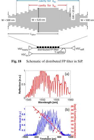
We have also implemented a distributed FP filter in SiP based on two spatially offset Bragg gratings with opposite chirp, see. Figure 18. As before, the Si waveguides have a thickness of 220 nm on top of a 3 μm BOX layer on a Si substrate and are covered by an index-matched 2μm top ox- ide cladding. Each chirped Bragg grating hasΛ =315 nm, ΔW = 10 nm, and 500 periods; the waveguide width W varies linearly from 500 nm to 520 nm from one end of the grating to the other (corresponding to a grating chirp of
|C1|=|C2|=12.2 nm/mm). The two gratings are separated by a lengthL=457.5μm. We use the reflection response, which is extracted via a Y-splitter. Again, VGCs are used to couple light into and out of the chip.
Figure 19 shows the measured response of the dis- tributed FP filter in SiP; the FSR clearly increases with in- creasing wavelength. We then implemented the filter in the waveform generation system. Pulses from a passively mode-locked fiber laser are filtered so that we operate over a wavelength range of ∼16 nm of the distributed FP filter response. We used 5 km of SMF as the dispersive medium for wavelength-to-time mapping. This results in a chirped microwave waveform with a total duration of∼1,100 ps and a chirp rate of 0.012 GHz/ps, see Fig. 19.
Integrated spectral shapers based on ring resonators have also been proposed and realized. For example, Fig. 20
Fig. 17 Generating chirped microwave waveforms with an integrated spectral shaper based on a Sagnac loop incorporating a chirped Bragg grat- ing. Response of the spectral shaper showing input optical pulses tuned to capture (a) increasing and (b) decreasing FSR. Corresponding tempo- ral waveforms after linear wavelength-to-time mapping and instantaneous frequency vs. time.
Fig. 18 Schematic of distributed FP filter in SiP.
Fig. 19 Spectral response (in reflection) of distributed FP filter in SiP.
Corresponding temporal waveform after wavelength-to-time mapping and instantaneous frequency vs. time.
Fig. 20 Schematic of tunable integrated spectral shaper in SiP based on cascaded microring resonators with additional MZ structures (courtesy of M. Qi).
Fig. 21 Schematic of integrated spectral shaper in SiP based on cascaded microring resonators embedded within an MZI (courtesy of J. Yao).
illustrates a spectral shaper based on 8 cascaded micror- ing resonators[52]. The spectral separation between the re- sponse of consecutive rings is ∼1.3 nm and each ring has an FSR of ∼16 nm. By tuning the resonant wavelengths and coupling strengths of each microring resonator (using microheaters placed above each ring for independent con- trol of the resonant wavelength and incorporating an MZ structure with microheaters at the through port of each ring to control the depth of the resonance), full reconfiguration of the spectral shaper is possible (at the through port, the wavelengths and amplitudes of the ‘slices’ from each ring can be controlled). Using this integrated device to shape the broadband pulses from a passively mode-locked laser, chirped microwave waveforms centered about 8 GHz with a chirp of 0.008 GHz/ps were synthesized[52].
Recently, a different version of an integrated spectral shaper using cascaded microring resonators was reported in [53]. In this case, the microring resonators are embedded in an MZI. Moreover, the microring radii differ substan- tially in order to provide a larger variation in the spectral separation between rings (see Fig. 21). The device operates in reflection mode so that the input and output can share a common VGC and the MZI configuration increases stabil- ity. As a proof-of-principle demonstration, devices based on 4 or 5 rings were fabricated and tested. Chirped microwave waveforms with bandwidths of 8.5 GHz and 15.5 GHz with chirp rates of 0.012 GHz/ps and 0.017s GHz/ps were achieved after linear wavelength-to-time mapping in a dis- persive medium with−948 ps/nm dispersion. These chirp rates are ten times greater than those obtained in[52]. While this prototype device was static, it can be readily adapted to allow for reconfigurable operation using thermal tuning as in[52]. Note that in both approaches, the number of cycles in the waveforms is constrained to the number of cascaded microrings. In many practical applications, a larger number of cycles is necessary which in turn, requires the addition of
microrings.
In Sect. 2, we described some recent developments for implementing tunable delays in SiP; these can be readily combined with the spectral shapers described here to realize a fully integrated chirped microwave waveform generation system. However, the main challenge resides in obtaining the necessary dispersion and/or bandwidth for appropriate wavelength-to-time mapping.
4. Summary and Perspectives
We have described the generation of UWB and RF wave- forms based on microwave photonic filtering as well as chirped microwave waveforms using optical spectral shap- ing followed by wavelength-to-time mapping. It should be noted that many of the MPF structures described in the re- view articles[9]–[12]can be employed for waveform gen- eration; we have presented only results in which the filters were used explicitly for such a purpose. We have also de- scribed briefly the implementation in SiP of a number of critical building to realize MPFs or spectral shapers. While several challenges still remain, e.g., the development of de- lay lines with larger bandwidth-delay products or filters that can process a larger number of taps, integrated microwave photonics is still an emerging field. SiP holds significant promise to realize a number of component technologies and integrated systems for demonstrating enhanced capability or functionality which, in turn, will pave the way for new ap- plications that will make the technology further commer- cially viable. Combined with recent advances in graphene microwave photonics[54], an exciting future undoubtedly lies ahead.
Acknowledgments
This research was supported in part by the Natural Sciences and Engineering Research Council (Canada), the Canadian Microelectronics Corporation, and the Fonds de recherche- Nature et technologies (Qu´ebec). I thank Rhys Adams (CEGEP Vanier College); Dr. Reza Ashrafi, Junjia Wang, Ming Ma, Mohammad Rezagholipour Dizaji, and Prof.
Martin Rochette (McGill University); and Mina Spasojevic and Jia Li (Ciena) for their contributions to this work.
The SiP devices presented in this paper were fabricated by Richard Bojko at the University of Washington Nanofabri- cation Facility, a member of the NSF National Nanotechnol- ogy Infrastructure Network.
References
[1] S. Pan and J. Yao, “UWB-over-fiber communications: modulation and transmission,” IEEE/OSA J. Lightw. Technol., vol.28, no.16, pp.2445–2455, Aug. 2010.
[2] D.K. Barton, Radar System Analysis and Modeling, Artech House, Boston, MA, 2005.
[3] J. Yao, “Microwave photonics,” IEEE/OSA J. Lightw. Technol., vol.27, no.3, pp.314–335, Feb. 2009.
[4] J. Yao, “Photonic generation of microwave arbitrary waveforms,”
Opt. Commun., vol.284, no.15, pp.3723–3736, July 2011.
[5] D. Marpaung, C. Roeloffzen, R. Heideman, A. Leinse, S. Sales, and J. Capmany, “Integrated microwave photonics,” Lasers & Photon.
Rev., vol.7, no.4, pp.506–538, July 2013.
[6] S. Koehl, A. Liu, and M. Pannicia, “Integrated silicon photonics:
harnessing the data explosion,” Opt. Photon. News, vol.22, no.3, pp.24–29, 2011.
[7] M. Streshinsky, R. Ding, Y. Liu, A. Novack, C. Galland, A.E.-J.
Lim, P.G.-Q. Lo, T. Baehr-Jones, and M. Hochberg, “The road to af- fordable, large-scale silicon photonics,” Opt. Photon. News, vol.24, no.9, pp.32–39, 2013.
[8] A.M. Weiner, “Ultrafast optical pulse shaping: A tutorial review,”
Opt. Commun., vol.284, no.15, pp.3669–3692, July 2011.
[9] J. Capmany, B. Ortega, D. Pastor, and S. Sales, “Discrete-time op- tical processing of microwave signals,” IEEE/OSA J. Lightw. Tech- nol., vol.23, no.2, pp.702–723, Feb. 2005.
[10] J. Capmany, B. Ortega, and D. Pastor, “A tutorial on microwave photonic filters,” IEEE/OSA J. Lightw. Technol., vol.24, no.1, pp.201–229, Jan. 2006.
[11] J. Capmany, J. Mora, I. Gasulla, J. Sancho, J. Lloret, and S. Sales,
“Microwave photonic signal processing,” IEEE/OSA J. Lightw.
Technol., vol.31, no.4, pp.571–586, Feb. 2013.
[12] R. Minasian, E.W.H. Chan, and X. Yi, “Microwave photonic sig- nal processing,” Opt. Express, vol.21, no.19, pp.22918–22936, Sept.
2013.
[13] M. Bolea, J. Mora, B. Ortega, and J. Capmany, “Optical UWB pulse generator using anNtap microwave photonic filter and phase inver- sion adaptable to different pulse modulation formats,” Opt. Express, vol.17, no.7, pp.5023–5032, March 2009.
[14] M. Bolea, J. Mora, B. Ortega, and J. Capmany, “High-order UWB pulses scheme to generate multilevel modulation formats based on incoherent optical sources,” Opt. Express, vol.21, no.23, pp.28914–28921, Nov. 2013.
[15] M. Rius, M. Bolea, J. Mora, B. Ortega, and J. Capmany, “Multi- band-UWB signals generation based on incoherent microwave pho- tonic filters,” IEEE Photon. Technol. Lett., vol.26, no.2, pp.142–145, Jan. 2014.
[16] M. Bolea, J. Mora, B. Ortega, and J. Capmany, “Photonic arbitrary waveform generation applicable to multiband UWB communica- tions,” Opt. Express, vol.18, no.25, pp.26259–26267, Dec. 2010.
[17] J. Mora, B. Ortega, A. D´ıez, J.L. Cruz, M.V. Andr´es, J. Capmany, and D. Pastor, “Photonic microwave tunable single-bandpass filter based on a Mach-Zehnder interferometer,” IEEE/OSA J. Lightw.
Technol., vol.24, no.7, pp.2500–2509, July 2006.
[18] R. Adams, R. Ashrafi, J. Wang, M.R. Dizaji, and L.R. Chen, “RF-ar- bitrary waveform generation based on microwave photonic filter- ing,” IEEE Photon. J., vol.6, no.5, 5501208, Oct. 2014.
[19] B. Vidal, J. Palac´ı, and J. Capmany, “Reconfigurable photonic mi- crowave filter based on four-wave mixing,” IEEE Photon. J., vol.4, no.3, pp.759–764, June 2012.
[20] L.R. Chen, J. Li, M. Spasojevic, and R. Adams, “Nanowires and sidewall Bragg gratings in silicon as enabling technologies for microwave photonic filters,” Opt. Express, vol.21, no.17, pp.19624–19633, Aug. 2013.
[21] Q. Zhong, V. Veerasubramanian, Y. Wang, W. Shi, D. Patel, S.
Ghosh, A. Samani, L. Chrostowski, R. Bojko, and D.V. Plant, “Fo- cusing-curved subwavelength grating couplers for ultra-broadband silicon photonics optical interfaces,” Opt. Express, vol.22, no.15, pp.18224–18231, July 2014.
[22] C. Wang and J. Yao, “Chirped microwave pulse compression using a photonic microwave filter with nonlinear phase response,” IEEE Trans. Microw. Theory and Techn., vol.57, no.2, pp.496–504, Feb.
2009.
[23] M. Bolea, J. Mora, L.R. Chen, and J. Capmany, “Highly chirped reconfigurable microwave photonic filter,” IEEE Photon. Technol.
Lett., vol.23, no.17, pp.1192–1194, Sept. 2011.
[24] C. Wang and J. Yao, “A nonuniformly spaced microwave photonic
filter using a spatially discrete chirped FBG,” IEEE Photon. Technol.
Lett., vol.25, no.19, pp.1889–1892, Oct. 2011.
[25] T. Tsuchizawa, K. Yamada, T. Watanabe, H. Shinojima, H. Nishi, and S. Itabashi, “Ultrasmall Silicon photonic devices and integration technology toward photonic-electronic convergence,” NTT Techni- cal Review, vol.8, no.2, pp.1–6, Feb. 2010.
[26] A. Rylyakov, C. Schow, B. Lee, W. Green, J. Van Campenhout, M.
Yang, F. Doany, S. Assefa, C. Jahnes, J. Kash, and Y. Vlasov, “A 3.9 ns 8.9 mW 4×4 Silicon photonic switch hybrid integrated with CMOS driver,” Proc. ISSSC, San Francisco, CA, pp.222–224, Feb.
2011.
[27] S. Cheung, T. Su, K. Okamoto, and S.J.B. Yoo, “Ultra-compact Sil- icon photonic 512×512 25 GHz arrayed waveguide grating router,”
IEEE J. Sel. Topics in Quantum Electron., vol.20, no.4, 8202207, July/Aug. 2014.
[28] G.T. Reed, G. Mashanovich, F.Y. Gardes, and D.J. Thomson, “Sil- icon optical modulators,” Nature Photon., vol.4, pp.518–526, Aug.
2010.
[29] P. Dong, C. Xie, L. Chen, L.L. Buhl, and Y.-K. Chen, “112-Gb/s monolithic PDM-QPSK modulator in silicon,” Opt. Express, vol.20, no.26, pp.B624–B629, Dec. 2012.
[30] M.W. Geis, S.J. Spector, M.E. Grein, R.T. Schulein, J.U. Yoon, D.M.
Lennon, S. Deneault, F. Gan, F.X. Kaertner, and T.M. Lyszczarz,
“CMOS-Compatible all-Si high-speed waveguide photodiodes with high responsivity in near-infrared communication band,” IEEE Pho- ton. Technol. Lett., vol.19, no.3, pp.152–154, Feb. 2007.
[31] M.S. Hai, M.N. Sakib, and O. Liboiron-Ladouceur, “A 16 GHz sil- icon-based monolithic balanced photodetector with on-chip capaci- tors for 25 Gbaud front-end receivers,” Opt. Express, vol.21, no.26, pp.32680–32689, Dec. 2013.
[32] I. Giuntoni, D. Stolarek, D.I. Kroushkov, J. Bruns, L. Zimmermann, B. Tillack, and K. Petermann, “Continuously tunable delay line based on SOI tapered Bragg gratings,” Opt. Express, vol.20, no.10, pp.11241–11246, May 2012.
[33] I. Giuntoni, D. Stolarek, J. Bruns, L. Zimmermann, B. Tillack, and K. Petermann, “Integrated dispersion compensator based on apodized SOI Bragg gratings,” IEEE Photon. Technol. Lett., vol.25, no.14, pp.1313–1316, July 2013.
[34] S. Khan and S. Fathpour, “Demonstration of complementary apodized cascaded grating waveguides for tunable optical delay lines,” Opt. Lett., vol.38, no.19, pp.3914–3916, Sept. 2013.
[35] R. Yu, S. Cheung, Y. Li, K. Okamoto, R. Proietti, Y. Yin, and S.J.B. Yoo, “A scalable silicon photonic chip-scale optical switch for high performance computing systems,” Opt. Express, vol.21, no.23, pp.32655–32667, Dec. 2013.
[36] H.-W. Chen, A.W. Fang, J.D. Peters, Z. Wang, J. Bovington, D.
Liang, and J.E. Bowers, “Integrated microwave photonic filter on a hybrid silicon platform,” IEEE Trans. Microw. Theory Tech., vol.58, no.11, pp.3213–3219, Nov. 2010.
[37] E.J. Norberg, R.S. Guzzon, J.S. Parker, L.A. Johansson, and L.A.
Coldren, “Programmable photonic microwave filters monolithically integrated in InP/InGaAsP,” IEEE/OSA J. Lightw. Technol., vol.29, no.11, pp.1611–1619, June 2011.
[38] J. Sancho, J. Bourderionnet, J. Lloret, S. Combri´e, I. Gasulla, S.
Xavier, S. Sales, P. Colman, G. Lehoucq, D. Dolfi, J. Capmany, and A. De Rossi, “Integrated microwave filter based on a pho- tonic crystal delay line,” Nature Commun., vol.3, article 1075, DOI:
10.1038/ncomms2092, Sept. 2012.
[39] B. Morrison, D. Marpaung, R. Pant, E. Li, D.-Y. Choi, S. Madden, B. Luther-Davies, and B.J. Eggleton, “Tunable microwave pho- tonic notch filter using on-chip stimulated Brillouin scattering,” Opt.
Commun., vol.313, pp.85–89, Feb. 2014.
[40] J. Chou, Y. Han, and B. Jalali, “Adaptive RF-photonic arbitrary waveform generation,” IEEE Photon. Technol. Lett., vol.15, no.4, pp.581–583, April 2003.
[41] I.S. Lin, J.D. McKinney, and A.M. Weiner, “Photonic synthesis of broadband microwave arbitrary waveforms applicable to ultra-wide-
band communication,” IEEE Microw. and Wireless Compon. Lett., vol.15, no.4, pp.226–228, April 2005.
[42] H. Chi, F. Zeng, and J. Yao, “Photonic generation of microwave sig- nals based on pulse shaping,” IEEE Photon. Technol. Lett., vol.19, no.9, pp.668–670, May 2007.
[43] M.A. Muriel, J. Aza˜na, and A. Carballar, “Real-time Fourier trans- former based on fiber gratings,” Opt. Lett., vol.24, no.1, pp.1–3, Jan.
1999.
[44] C. Wang and J. Yao, “Photonic generation of chirped millime- ter-wave pulses based on nonlinear frequency-to-time mapping in a nonlinearly chirped fiber Bragg grating,” IEEE Trans. on Microw.
Theory and Techn., vol.56, no.2, pp.542–553, Feb. 2008.
[45] H. Chi and J. Yao, “Chirped RF pulse generation based on optical spectral shaping and wavelength-to-time mapping using a nonlin- early chirped fiber Bragg grating,” IEEE/POSA J. Lightw. Technol., vol.26, no.10, pp.1282–1287, May 2008.
[46] C. Wang and J. Yao, “Photonic generation of chirped microwave pulses using superimposed chirped fiber Bragg gratings,” IEEE Pho- ton. Technol. Lett., vol.20, no.11, pp.882–884, June 2008.
[47] C. Wang and J. Yao, “Chirped microwave pulse generation based on optical spectral shaping and wavelength-to-time mapping using a Sagnac loop mirror incorporating a chirped fiber Bragg grating,”
IEEE/OSA J. Lightw. Technol., vol.27, no.16, pp.3336–3341, Aug.
2009.
[48] R. Slav´ık, S. Doucet, and S. LaRochelle, “High-performance all-fiber Fabry-P´erot filters with superimposed chirped Bragg grat- ings,” IEEE/OSA J. Lightw. Technol., vol.21, no.4, pp.1059–1065, April 2003.
[49] X. Shu, L. Yu, D. Zhao, L. Zhang, K. Sugden, and I. Bennion,
“Transmission characteristics of Sagnac interferometers based on fiber Bragg gratings,” J. Opt. Soc. Am. B, vol.19, no.11, pp.2770–2780, Nov. 2002.
[50] W. Wang, W. Shi, R. Vafei, N.A.F. Jaeger, and L. Chrostowski,
“Uniform and sampled Bragg gratings in SOI strip waveguides with sidewall corrugations,” IEEE Photon. Technol. Lett., vol.23, no.5, pp.290–292, March 2011.
[51] J.T. Hastings, M.H. Lim, J.G. Goodberlet, and H.I. Smith,
“Optical waveguides with apodized sidewall gratings via spa- tial-phase-locked electron-beam lithography,” J. Vac. Sci. Technol.
B, vol.20, no.6, pp.2753–2757, Dec. 2002.
[52] M.H. Khan, H. Sehn, Y. Xuan, L. Zhao, S. Xiao, D.E. Leaird, A.M.
Weiner, and M. Qi, “Ultrabroadbandwidth arbitrary radiofrequency waveform generation with a silicon photonic chip-based spectral shaper,” Nat. Photonics, vol.4, pp.117–122, Jan. 2010.
[53] W. Zhang, J. Zhang, and J. Yao, “Largely chirped microwave waveform generation using a silicon-based on-chip optical spectra shaper,” Proc. Int. Top. Meeting on Microwave Photonics/9thAsia- Pacific Microwave Photonics Conference, Sapporo, Japan, paper TuC-6, pp.51–53, 20-23 Oct. 2014,.
[54] J. Capmany, D. Dom´enech, and P. Mu˜noz, “Graphene integrated mi- crowave photonics,” IEEE/OSA J. Lightw. Technol., vol.32, no.20, pp.3785–3796, Oct. 2014.
Lawrence R. Chen received the BEng in Electrical Engineering and Mathematics from McGill University in 1995 and the MASc and PhD degrees in Electrical and Computer Engi- neering from the University of Toronto in 1997 and 2000, respectively. He returned to McGill University in 2000, where he is a Professor in the Department of Electrical and Computer En- gineering. His research interests are in optical and microwave signal processing, silicon pho- tonics, and teaching pedagogy. He is currently Editor-in-Chief of theIEEE Photonics Society Newsletterand an Editor of Optics Communications. He is a Fellow of the Optical Society of America.

![Figure 3 illustrates several different MPF implementations and the overall system for generating IR-UWB and MB-UWB waveforms [13]–[16]](https://thumb-ap.123doks.com/thumbv2/123deta/5625246.1500135/3.892.467.821.115.596/figure-illustrates-different-mpf-implementations-overall-generating-waveforms.webp)
![Fig. 4 Pulse doublet generated using (a) the MPF from Fig. 3 (a) (after [13]) and (b) the MPF from Fig](https://thumb-ap.123doks.com/thumbv2/123deta/5625246.1500135/4.892.465.816.107.401/fig-pulse-doublet-generated-using-mpf-from-after.webp)