理論集光効率 63%
InAs 量子ドットを利用した高効率太陽電池
現在,最も普及している Si 材料を主体とした単接合 型太陽電池では,太陽光のうちバンドギャップ以上のエ ネルギーを有する光子は,吸収した後そのエネルギーが 熱に変換される.一方,バンドギャップ以下のエネルギー の光子は透過してしまい光電変換ができない.これらの 損失要因はトレードオフの関係にあり,エネルギー変換 効率は非集光下で約 30%,最大集光下において約 40%に制限される.このような背景のもと,太陽電池に 中間バンドを設けて高効率化を図る,中間バンド型太 陽電池が注目されている.この太陽電池ではバンドギャ ップの中間に形成される中間バンドを利用した 2 段階の 光吸収を行うことで,太陽光スペクトルとの整合性を向 上させることができる(図 1b).中間バンド型太陽電池の 非集光時における理論的な変換効率は,バンドギャッ プ・エネルギー(EG)が 2.4eV で伝導帯と中間バンド間 のエネルギー差(ECI)が 0.9eV のときに約 47%にな る.理論上可能な最大の集光倍率である約 4 万 6200 倍 集 光 の 場 合 は , EG= 1.9eV , ECI = 0.7eV の組み合わせのときに最も高い 63%の変換効率 に達する[1].バンドギャップ・エネルギーの変化に対する 変換効率の減少は,既存の結晶 Si 型太陽電池に比 べて緩やかである.例えば最大集光時には,EGが 1.4 2.6 eV の広い範囲で 60%以上の変換効率を得る 設計が可能になる(図 2). 中間バンドを形成する方法の一つとして,我々は半 導体量子ドットを用いる方法を研究している.量子ドット は, 直径が数十 nm と小さいナノ構造の周囲を十分に 高いポテンシャル障壁で囲んだ形を成しており,電子を 3 次元全ての方向に閉じ込めることができる(図 3a).この (a) (b) 図 1.(a)既存の太陽電池, (b)中間バンド型太陽電池 の動作原理 図 2.ホスト材料のバンドギャップに対する既存の太陽 電池と中間バンド型太陽電池の変換効率の変化研究紹介
ため,量子ドット内の電子は原子のような完全に離散化 したエネルギー状態を有する.このような量子ドットを高 密度に規則配列させると,量子ドット間が電子的に結 合してバンドを形成する.すなわち,図 3b に示すような 3 次元配列した量子ドットを太陽電池に導入することに より,中間バンド型太陽電池を実現することが可能とな る. 量子ドットの形成方法として,我々は結晶成長の成 長モードの一つである Stranski-Krastanov(S-K)法を 用いている.この成長モードでは結晶の格子定数差を 利用して 3 次元の島状構造が自己形成される.代表 的な例が GaAs 基板上への InAs 材料の結晶成長で ある.InAs 結晶の格子定数は GaAs よりも 7.2%大 きく,成長初期では層状に結晶が成長するが,その後, 成長膜が厚くなると歪みにより島状に結晶が成長する (図 4a, 4b).図 4c は GaAs(001)基板上に成長し た InAs 量子ドットの AFM 像を示している.S-K 成長 モードの量子ドットはボトムアップ方式の自己形成過程の た め , エ ッ チ ン グ 等 の ト ッ プ ダ ウ ン 方 式 の 加 工 技 術 に比べて高品質な結晶が得られるというメリットがあるが, 形成位置の制御が困難であるということが問題とされる. これに対して,我々は量子ドットを作製する際の基板方 位として GaAs(311)B 基板を用いることに着目した. 図 4b は GaAs(311)B 基板上に成長した InGaAs 量 子ドットの AFM 像を示している.GaAs(311)B 基板は 面内に特異な歪み場を有しており,面内配列した量子 ドットが自己組織的に形成させることができる. 中間バンド型太陽電池への応用として,十分な光吸 収体積を得るには量子ドットを積層させることが必要とな る.しかしながら,前述のとおり S-K 成長法では歪みエ ネルギーを利用して量子ドットを形成するため,基板材 料と同じ GaAs を埋め込み材料(中間層)として用い た場合,積層するに従って歪みが蓄積する.残留する 歪み場は上層へ放射状に伝搬し,その結果,量子ドッ トのサイズが徐々に増大し,さらには結晶欠陥を生じさ せ,太陽電池の特性を大きく劣化させることになる.そこ で,我々は中間層に基板材料よりも格子定数の小さい GaNAs 材料を用いることで,量子ドットとは逆向きの方 図 3.(a)孤立量子ドット,(b)3 次元量子ドット超格子の 概念図とバンド構造 図 4.(a)S-K 成長モードの概念図, (b)InAs 量子ドット を GaAs 層で埋め込んだ構造の断面 TEM 写 真, (c) GaAs(001)基板上に作製した InAs 量子 ドットの AFM 像, (d)GaAs(311)B 基板上に作製 した InGaAs 量子ドットの AFM 像の量子ドットを積層することに成功している. 図 6 は GaAs 基板において,歪み補償法を用いて 20, 30, 及び 50 層の InAs/GaNAs 量子ドットを導入した 太陽電池の量子効率の測定結果を示している.波長 880 nm までの GaAs 層による吸収に加えて,950 nm 付近にピークを持つ光電流の寄与は量子ドットの埋 とともにその吸収量を増大させることが可能である. 中間バンド型量子ドット太陽電池では,中間バンドか ら伝導帯への電子の励起は,光吸収による成分が支配 的に生じ、熱励起による成分は極力抑えられていること が重要となる.そこで我々は,中間バンドを介した 2 段 階の光吸収を評価するための新たなシステム(図 7)を構 築した.本測定系では,単色光を用いて量子効率を 測定する際に,太陽光スペクトルのうち波長 1400 nm 以上の赤外光を照射しながらスキャンすることができる. このとき,赤外光の照射時と非照射時における量子効 率の差分を取ることで,中間バンドから伝導帯に光学的 に遷移した成分の電流量を評価することができる. また,2 段階光吸収を増大させる方法として,量子ド ットに Si を直接ドーピングする方法を開発した.量子ドッ ト層にドーピングを行わない従来の量子ドット太陽電池で は,中間バンド内のキャリア占有率が低く,2 段階の光 (a) (b) 図 5. (a)既存の太陽電池, (b)中間バンド型太陽電 池の動作原理 図 6.歪み補償 InAs/GaNAs 量子ドット太陽電池の量 子効率における積層数依存性 図 7. 赤外光を用いた 2 段階光吸収評価システム
研究紹介
吸収が起こる割合が極めて低い状態にある.量子ドット に Si をドーピングすると,余剰電子が生成され,予め中 間バンド内にキャリアがある程度占有した状態を作ること ができ,2 段階光吸収が増大されると考えた.図 8 は InAs/GaNAs 量子ドット太陽電池において量子ドットに Si を直接ドーピングした効果を検証した結果である.Si を直接ドーピングした量子ドット太陽電池において 2 段階 光吸収による電流生成を観測することに成功した[2].こ れまで,量子ドット太陽電池の 2 段階光吸収は,36 K の低温動作においては報告[3]されていたが,室温での 実証例はなく,本結果が世界初の報告となる. 結晶成長技術の研究開発により,我々は量子ドット 太 陽 電池の 変 換効 率 を 72 倍の 集光 下に おい て 26.8%まで向上させることに成功した(図 9).しかしな がら,現状の変換効率は理論値をはるかに下回っている. この原因としては,(1) 量子ドットによる光吸収量が少 ないこと,(2) 2 段階光吸収レートが低いことが挙げられ る.効率改善には,量子ドットの高密度化及び,バン ド構造のさらなる最適化が鍵となる. 参考文献[1]A. Luque, and A. Martí, "Increasing the Efficiency of Ideal Solar Cells by Photon Induced Transitions at Intermediate Levels", Phys. Rev. Lett., vol. 78, 5014-5017 (1997). [2]Y. Okada, T. Morioka, K. Yoshida, R. Oshima, Y. Shoji, T.
Inoue, and T. Kita, "Increase in photocurrent by optical transitions via intermediate quantum states in direct-doped InAs/GaNAs strain-compensated quantum dot solar cell,"J. Appl. Phys., vol. 109, 024301 (2011).
[3] A. Martí, E. Antolín, C. R. Stanley, C. D. Farmer, N. López, P. Días, E. Cánovas, P. G. Linares, and A. Luque, "Production of Photocurrent due to Intermediate-to- Conduction-Band Transitions: A Demonstration of a Key Operating Principle of the Intermediate-Band Solar Cell," Phys. Rev. Lett., vol. 97, 247701 (2006).
図 8.(a)従来の量子ドット太陽電池,(b)Si を直接ドーピ ングした量子ドット太陽電池の 2 段階吸収特性
図 9.高電圧低電流型量子ドット太陽電池の I-V 特性 (上図)と集光特性(下図)
A way to highly efficient cost
effective solar cell
Background
Due to an increasing demand for a transition to renewable energy technologies, highly efficient third-generation solar cells have received a lot of attention. A recent report has successfully demonstrated a high conversion efficiency of 44% in a multi-junction solar cell (MJSC). In theory, under 1 sun irradiance, a single solar cell only converts 30% of the solar energy, a tandem structure of two cells can convert 42%, a tandem structure of three cells can convert 49%, etc. Under the highest possible light concentration, these efficiencies are 40% (one cell), 55% (two cells), 63% (three cells), etc. The lowest efficiency for a single junction solar cell such as Si is mainly due to the losses in two ways of absorbed photon energies from sunlight. The extra energy of photons having an energy higher than the bandgap is converted into heat. Meanwhile, photoelectric conversion is not possible for photons of energy smaller than the band gap. These trade-off losses can be limitted with increasing number of junctions with different band gaps in a multi-junction tandem structure. However, in addition to the challenges of the tunnel junction materials for electrical connection between cells and the optimal compound materials in each cell, an increase in manufacturing cost is inevitable.
A cost-effective alternative to MJSC is the class
of intermediate band solar cells (IBSC), where intermediate bands inside the conventional band-gaps of semiconductors effectively works as multiple channels to absorb wide range of photons of the solar spectrum as a MJSC does with its multiple cells. Theoretical calculation predicted a conversion efficiency of 63% at maximal solar concentration for a three-band IBSC, and this value of efficiency is 2-3 times higher than that of current single-crystal Si solar cells.
Requirements for an IBSC
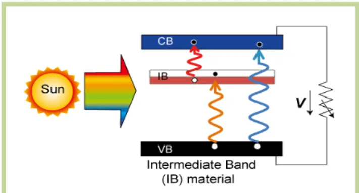
Shown in Fig. 1 is the schematic diagram of an IBSC. An intermediate band (IB) located between the conduction and valence bands (CB and VB) divides the semiconductor bandgap EG into two
bandgaps EIV and ECI. In a practical IBSC, IB
material is sandwiched between two conventional semiconductors of p and n type. The potential of this cell is equivalent to a three-junction solar cell
研究紹介
but without the requirement for tunnel junctions. Its practical implementation requires: (1) An IB material, to which it is possible to manufacture appropriate contacts (the p and n emitters). (2) The absorption of two sub-bandgap photons. One photon pumps an electron from the VB to the IB and a second photon pumps an electron from IB to the CB. (3) Carrier relaxation between bands has to occur at a much lower rate than carrier relaxation within bands. This allows the existence of three distinguishable quasi-Fermi levels associated with each of the bands in an IBSC. Approaches toward IB material fabrication
At present, there are two directions for the development of IB material; (1) Quantum nano-structure, such as Quantum dot (QD) and (2) thin films. In the QD approach, the IB arises for the energy levels corresponding to the electrons confined in the dots. In this digest of Okada Laboratory, there are other articles on this approach using III-V systems as InAs QD/GaAs, and details of this approach can be found therein. The class of thin film IBSC can be classified into two groups depending on the nature of the formation of intermediate bands (IB in Fig. 1): (1) Impurity band approach, and (2) Highly mismatched alloy (HMA) approach.
In the class of impurity band IBSC, the energetic position of the IB band can be defined by the position of impurity bands inside the host
semiconductor. When impurities of deep states are incorporated in a high amount, an impurity band is formed between the energy gaps of the host materials, and can be effectively designed as IB materials. Some of the reported material systems for this purpose are, for example, Ti doped Si, Ti doped GaAs, and transition metals (Ti, V, Cr. Ni, Fe, etc) doped CuInGaS2 etc.
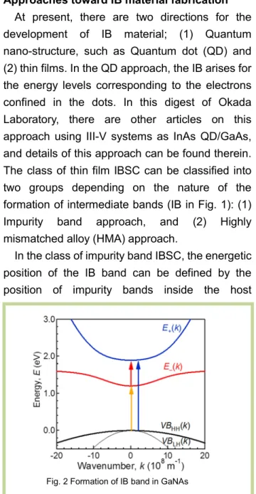
The other approach is based on HMA materials such as (ZnMnTe-O, GaAs-N, etc.). The electronic band structure of the HMA system is described by the band anti-crossing (BAC) model, which is an anti-crossing interaction between localized states of isoelectric dopants (N in GaAs and O in ZnTe) and the extended states of the host matrix. This interaction splits the conduction band in two subbands, a lower subband (E−) which can be
adopted for an IB and a higher subband (E+)
adopted for CB (shown in Fig. 2). The advantage of this approach lies in the freedom of tunability of the IB position by the amount of isoelectric dopants.
Thin film IBSC based on GaNAs(Sb) HMA As discussed, the key requirement for a proper operation of IBSC is an efficient excitation of electron-hole pairs with two below bandgap photons. Therefore, the experiment of the direct observation of production of photocurrent due to two-photon excitation (TPE) is required to demonstrate the IB activity in an IBSC.
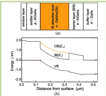
For this purpose, structures containing GaNAs and GaNAsSb absorbers were grown using radio-frequency plasma assisted molecular beam epitaxy (RF-MBE). Sb atoms are incorporated to improve the GaNAs material quality. Band diagrams were calculated using a Poisson equation solver. In these structures, namely the blocked intermediate band (BIB) structures, the backside n-AlGaAs layers were lightly doped providing a good barrier blocking the electrical contact between the IB and the GaAs substrate. Window layer on the top prevents carrier from
unblocked intermediate band (UIB) structure was fabricated in which the backside AlGaAs layer was heavily doped resulting in a thin electrically transparent barrier between the IB in GaNAs layer and the n-GaAs substrate.
QE, TPE experiment and Model Analysis The External quantum efficiency (EQE) spectra of the BIB structures are shown in Fig. 4 (a). The spectral features are identical in both of the structures except that an extended spectral response up to 1150 nm from the GaNAsSb BIB. These data are in agreement with VB→IB(E−)
transitions in PR spectra (not shown here).
IB(E−)→CB(E+) transition has been obtained in
TPE experiments using two optical sources, which are an infrared (IR) and a monochromatic source. With the monochromatic source “ON”, switching “ON” the IR illumination enables IB(E−)→CB(E+)
transitions, resulting in an increased photocurrent through two photon transfer of electrons from VB to CB(E+) via the IB(E−).
The ∆QE spectra of the TPE experiments are shown in Fig. 4 (b). In the UIB structure, there is no additional photocurrent associated with the IR illumination. In both of the IBSC structures, the
Fig. 4 (a) and (b) are EQE and ∆QE spectra respectively, for GaNAs and GaNAsSb BIB.. ∆QE of UIB structure is also shown in (b).
Fig. 5 (a) PR spectrum of GaNAs sample (b) Schematic transition diagram for TPE.
研究紹介
excess electrons trapped in the IB(E−) are excited
to CB(E+) with IR photons producing an additional
photocurrent that effectively results from two photons producing one electron-hole pair. The enhancement in the ∆QE value of the GaNAsSb IBSC above the VB → CB(E+) transitions by a
factor of 2 suggests improved IB(E−) → CB(E+)
transitions with IR photons producing an additional photocurrent.
Details of the photocurrent production in ∆QE spectra can be analyzed in terms of 3 transitions evident in the PR spectrum in Fig. 5 (a) and schematically shown in Fig. 5(b). The enhanced photocurrent production in the GaNAsSb IBSC can be attributed to the enhanced IB(E−)
→ CB(E+) transitions due to improved material
quality.
Solar Cell Performance
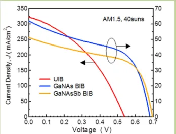
The current density-voltage (J−V) characteristics measured at room temperature under 40 suns of AM1.5 solar spectrum are shown in Fig. 6. The VOCin the GaNAsSb BIB structure is
somewhat improved compared to that in the GaNAs BIB. Despite a lower bandgap in GaNAsSb BIB than the GaNAs by 60 meV, the larger VOC in the GaNAsSb is likely due to the
reduction of electron traps, which also resulted in
the increase of effective electron concentration. The reduction in the photocurrent for GaNAsSb BIB structure in Fig. 6 can be attributed to reduced field-assisted carrier collection in the short wavelength region compared to the GaNAs BIB agreeing with EQE spectra in Fig. 4(a). The increased carrier concentration in the GaNAsSb IB(E−) is the origin of the narrowed depletion
width.
Key Issues for improvements
For low JSC values, one of the issues is
insufficient optical transition rate from the IB(E−) to
the CB(E+) band. To resolve this issue, a suitable
electron filling of the IB band has been theoretically predicted to generate improved photocurrent. Another issue is insufficient carrier collection due to short minority carrier diffusion lengths. Optimization of key parameters governing the material quality can lead to improvement of the carrier mobility and lifetime, and thus the improvement in carrier diffusion length.
Reference
[1] N. Ahsan, N. Miyashita, M. M. Islam, K. M. Yu, W. Walukiewicz, and Y. Okada, “Two-photon excitation in an intermediate band solar cell structure,” Appl. Phys. Lett. vol. 100, 172111 ( 2012).
[2] N. Ahsan, N. Miyashita, M. M. Islam, K. M. Yu, W. Walukiewicz, and Y. Okada, “Effect of Sb on GaNAs Intermediate Band Solar Cells,”IEEE J. Photovolt. vol. 3, 730 ( 2013).
Fig. 6 Current density-voltage (J-V) characteristics under 40 suns of AM1.5 illumination.