Japan Advanced Institute of Science and Technology
JAIST Repository
https://dspace.jaist.ac.jp/Title
Resonant surface second harmonic generation from
Au films on NaCl(100)
Author(s)
Kitahara, T.; Tanaka, H.; Nishioka, Y.; Mizutani,
G.
Citation
Physical Review B, 64(19): 193412-1-193412-4
Issue Date
2001-10-25
Type
Journal Article
Text version
publisher
URL
http://hdl.handle.net/10119/4184
Rights
T. Kitahara, H. Tanaka, Y. Nishioka, G. Mizutani,
Physical Review B, 64, 193412, 2001. "Copyright
2001 by the American Physical Society."
http://link.aps.org/abstract/PRB/v64/e193412
Description
Resonant surface second harmonic generation from Au films on NaCl
„100…
T. Kitahara, H. Tanaka, and Y. NishiokaSchool of Materials Science, Japan Advanced Institute of Science and Technology Tatsunokuchi, Nomi-gun, Ishikawa 923-1292, Japan G. Mizutani*
School of Materials Science, Japan Advanced Institute of Science and Technology Tatsunokuchi, Nomi-gun, Ishikawa 923-1292, Japan and ‘‘Fields and Reactions,’’ PRESTO, Japan Science and Technology Corporation 4-1-8 Kawaguchishi-Honmachi,
Saitama 332-0012, Japan
共Received 7 March 2001; revised manuscript received 2 July 2001; published 25 October 2001兲
We have found that the resonance energy of optical second-harmonic共SH兲 generation from Au films on NaCl共100兲 depends strongly on the film thickness. The resonance peak of the SH intensity was found at 2ប⫽3.2 eV for the island film of mean thickness 0.4 nm, while it appeared at 2ប⫽2.4 eV for the continu-ous film of thickness 40 nm. We suggest that the SH intensity peak observed at 2ប⫽3.2 eV originates from a resonant transition from occupied to unoccupied electronic levels of the 共100兲 surface on top of the Au islands. The SH intensity peak observed at 2ប⫽2.4 eV for the film thickness of 40 nm originates from the roughness-induced linear dielectric property of the film.
DOI: 10.1103/PhysRevB.64.193412 PACS number共s兲: 73.20.At, 42.65.Ky
I. INTRODUCTION
Optical second-harmonic共SH兲 spectroscopy has become a useful tool for investigating surface and interface electronic levels. However, there are still a lot of problems about how to relate SH spectra to the profiles of surface and interface electronic levels. Concerning smooth noble-metal surfaces the SH response is understood to originate either from the free-electron gas described by a ‘‘jellium’’ model1 or from localized surface electronic levels.2,3However, no systematic understanding of the relative importance of various sources contributing to the observed nonlinearity has yet been reached.
It has been pointed out that the SH response of surfaces of Ag共110兲,2 polycrystalline Cu,3 and Cu共111兲4 cannot be ex-plained by the jellium model. For Ag共110兲 a SH intensity peak observed at ប⬃1.7 eV has been assigned to a reso-nance of a transition from occupied to unoccupied surface levels.2As for another important noble metal Au, we have observed a strong enhancement of SH intensity at 2ប
⫽2.5 and 5.0 eV from a glass-Au interface. We suggested
that the SH enhancement arises from the resonance of an interband transition from an occupied d band to an unoccu-pied s, p band of a glass-polycrystalline Au共111兲 interface.5 Hohlfeld et al. reported that a similar peak observed near 2ប⫽5.0 eV for a polycrystalline Au film is rather due to the structure of linear Fresnel factors.6There has also been a SH observation by Pedersen et al. on a quantum-confinement effect of electrons in epitaxial Au films at coverage less than 45 ML.7SH enhancement at 2ប⬃2.4 eV is also observed for 4 nm diameter Au clusters embedded in an alumina ma-trix and the peak is assigned to the surface-plasmon resonance.8However, no detailed SH spectroscopy has been performed on Au crystalline surfaces, although such mea-surement is necessary in order to clarify the character of the nonlinear response of localized d electrons systematically.
In this study, we have investigated how the face index of
Au surfaces influences the resonance energy of its surface-electronic states. For this purpose we have selected Au films deposited on NaCl共100兲. This selection is motivated by the fact that 共100兲, 共111兲 and polycrystalline surfaces of Au oc-cur successively on NaCl共100兲 as the film thickness is increased.9 Namely, at the substrate temperature of 400 °C and for the mean film thickness less than 0.4 nm, films with
共100兲 surfaces grow epitaxially on NaCl共100兲. When the
thickness increases, the 共111兲 surface component with ran-dom azimuthal orientation emerges. For the thickness of sev-eral tens of nanometers, the 共111兲 surface component disap-pears and a polycrystalline component becomes dominant. Hence this sample is very convenient for the purpose of checking whether there is a change in the resonance energy as a function of the face index. However, we must take care of the fact that this film grows in the Volmer-Weber mode at low thicknesses.
II. EXPERIMENT
NaCl共100兲 surfaces were obtained by cleavage in air and Au thin films were evaporated on them with a metal evapo-rator by electron-bombardment heating 共OMICRON EFM3兲 in an ultrahigh vacuum chamber with a base pressure of 3
⫻10⫺10Torr. The substrate temperature measured with a thermocouple attached to the sample holder was 400 °C and the deposition rate was⬃0.1 nm/min. During the deposition the chamber pressure was around 5⫻10⫺9Torr. The film thickness was monitored by a quartz-crystal microbalance. In order to obtain the nominal mean thickness, the measured thickness was multiplied by 0.6, the sticking probability of Au on NaCl at 400 °C.10The surface structures of the depos-ited films were characterized by reflection high-energy elec-tron diffraction共RHEED兲 and the surface morphology of the films was checked with an atomic-force microscope 共AFM, Nanoscope III Digital Instruments兲 with spatial resolution of 1 nm. The linear reflection spectra of the film were also
measured in air, using a tungsten lamp as a light source and a monochromator 共Jobin-Yvon HR-320兲.
The chamber is equipped with a tubulated viewport with a cylindrical quartz glass wall. For SH-generation共SHG兲 mea-surements the sample is transported into the cylindrical part of this viewport and the optical excitation and observation was done through the quartz glass wall. During the SHG measurements the sample was kept at room temperature.
The experimental setup for SHG measurements has been described elsewhere.5 The light source of the fundamental frequency was an optical parametric oscillator共Spectra Phys-ics MOPO-730兲 driven by a frequency-tripled Q-switched Nd:YAG laser 共Spectra Physics GCR-250兲, with a tunable wavelength in the visible and near-infrared regions. The spectral bandwidth of the laser beam was ⬃20 meV, the pulse duration time was⬃3 nsec, and the repetition rate was 10 Hz. The p-polarized fundamental light was directed onto the sample at the angle of incidence of 45° and the reflected SH light of all polarizations from the sample was collected. The plane of incidence was parallel to the关010兴 direction of the NaCl共100兲 substrate. A fraction of the incident laser light was split off from the beam and directed onto a reference sample 关共a兲 GaAs共100兲 wafer兴 and the reflected SH light from it was used to correct for the laser-intensity fluctuations.
III. RESULTS AND DISCUSSION
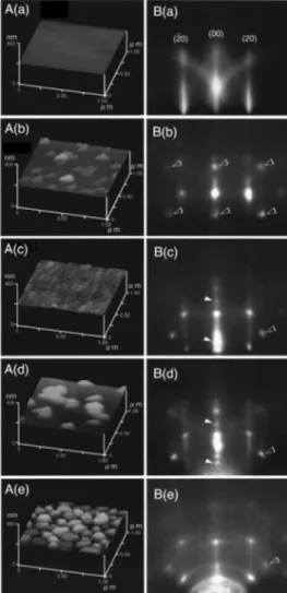
In Fig. 1 we show AFM and RHEED images of the Au films deposited on NaCl共100兲 substrates with various thick-nesses. Typically, NaCl共100兲 successfully cleaved gives smooth surface topography as shown in Fig. 1A共a兲 although we can also find step structures at other positions. The RHEED pattern of the cleaved NaCl共100兲 surface shows
共00兲, 共20兲, and (20¯) streaks as shown in Fig. 1B共a兲,
indicat-ing a smooth surface. For the Au film of mean thickness 0.4 nm, the AFM image 关Fig. 1A共b兲兴 shows isolated islands composed of small Au grains of height⬃20 nm and diameter
⬃60 nm. The corresponding RHEED pattern shows distinct 共100兲 spots of Au epitaxial component as are indicated by
open triangles in Fig. 1B共b兲. The fact that the diffraction from the Au共100兲 structure is observed as spots and the streaks from the substrate is still seen indicates that the Au layer grows in three-dimensional islands, consistent with the observation by AFM 关Fig. 1A共b兲兴. The other spots seen on the streaks are diffraction from the bulk NaCl induced by step structures. We have intentionally chosen the RHEED image including these spots to make the assignments of the spots from the Au film easier. For the Au film of the mean thickness 3.7 nm, the number of the islands observed by AFM is larger, but the sizes of the constituent grains are similar to those for the film of the mean thickness 0.4 nm
关Fig. 1A共c兲兴. The corresponding RHEED pattern shows spots
indicating the coexistence of Au共111兲 surfaces with random azimuthal orientation as are indicated by solid triangles in Fig. 1B共c兲. As a reference, RHEED spots expected from ep-itaxial Au共100兲 islands and the Au共111兲 polycrystalline do-mains with random azimuthal orientation on a NaCl共100兲 surface in the关001兴 azimuth are shown schematically in Fig.
2. For the Au film of the mean thickness 6.0 nm we see larger islands with the average height⬃80 nm and diameter
⬃250 nm 关Fig. 1A共d兲兴, but the RHEED pattern 关Fig. 1B共d兲兴
looks similar to that from the film of mean thickness 3.7 nm
关Fig. 1B共c兲兴. At the mean thickness 40 nm, the Au film is a
continuous film with surface roughness as shown in Fig. 1A共e兲. On the corresponding RHEED pattern 关Fig. 1B共e兲兴, we can see strong Debye rings indicating a polycrystalline structure but very weak 共100兲 spots, while the diffraction from the Au共111兲 surface component is not seen.
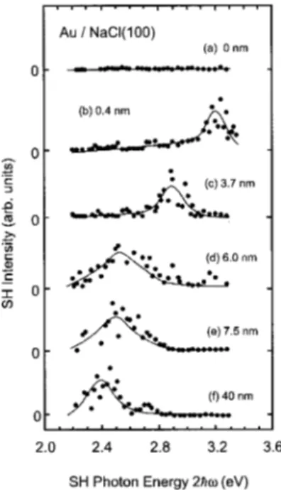
Figure 3 shows the SH intensity from Au thin films grown on NaCl共100兲 surfaces at various thicknesses as a function of the SH photon energy 2ប for p-polarized excitation. The SH intensity from the substrate NaCl共100兲 is very weak in the whole spectral region, as shown in Fig. 3共a兲. The SH intensity spectra from Au films of mean thicknesses 0.4, 3.7,
FIG. 1. AFM and RHEED images of the Au films deposited on NaCl共100兲 with various thicknesses. Panels 共a兲–共e兲 of part A are three-dimensional AFM images and panels 共a兲–共e兲 of part B are RHEED images. The mean thicknesses of the Au films are共a兲 0 nm,
共b兲 0.4 nm, 共c兲 3.7 nm, 共d兲 6.0 nm, and 共e兲 40 nm. The RHEED
patterns were taken in the 关001兴 azimuth and the energy of the incident electrons was 15 keV. Open triangles 共䉮兲 in the RHEED images indicate the spots from the epitaxial Au共100兲 structure. Solid triangles 共䉲兲 indicate the spots from the Au共111兲 structures with random azimuthal orientations.
BRIEF REPORTS PHYSICAL REVIEW B 64 193412
6.0, 7.5, and 40 nm have peaks at 2ប⬃3.2, 2.9, 2.5, 2.5, and 2.4 eV, respectively, as shown in Figs. 3共b兲–3共f兲.
Here we discuss the origins of the SH intensity peaks in Fig. 3. There are several candidate origins of the observed SH intensity peaks. They are the roughness-induced effective linear dielectric property of the film,11–15the ‘‘lightning-rod effect,’’16,17 the quantum-confinement effects of free-electron gas,7,18 the resonant radiation from the bulk dipoles19and higher-order multipoles,20and the resonance of surface-electronic levels.2The first two effects are related to the enhancement of the local electromagnetic field by the microscopic structures on the Au films. The others are asso-ciated with the enhancement of the nonlinear susceptibilities of the Au films themselves.19
First of all, we concentrate on the film of 40 nm thickness
关Fig. 3共f兲兴 and discuss the roughness-induced effective linear
dielectric property of the film as a candidate origin of the SH intensity peak. The film of 40 nm thickness is a continuous film, but it has a considerable roughness on the surface as can be seen in Fig. 1A共e兲. In order to check the possibility of this candidate origin, we have measured linear reflectance spectra of the same films 共not shown兲. For the Au film of mean thickness 40 nm, we have found a structure at 2.4 eV, the same energy as that of the SH intensity peak. It has been reported that change of dielectric property of Au occurs due to surface roughness or island structures.11,12 Mabuchi et al. have found a resonant absorption at 2.34 eV for Au particles with a diameter of 30 nm.13Palpant et al. have also found a blueshift of the absorption resonance with decreasing cluster size, from 2.33 eV for size 3.7 nm to 2.52 eV for size 2.0 nm.15Furthermore, Antoine et al. have found a SH intensity peak at 2ប⬃2.4 eV from Au clusters of 4 nm diameters embedded in an alumina matrix and have suggested that surface-plasmon excitation is involved.8 Because the peak positions of the SH intensity and the linear reflectance of our
Au film of mean thickness 40 nm are roughly close to these energies, we infer that the peaks are caused by the roughness-induced effective linear dielectric property of the film.
On the other hand, the SH intensity peak at 3.2 eV for the mean thickness of 0.4 nm in Fig. 3共b兲 cannot be assigned to the roughness-induced effective linear dielectric property of the film. It might be possible that the energy of the roughness-induced linear dielectric structure shifts to the higher-energy side due to the size effect of the Au grains. However, the average height and diameter of the Au grains in the film of mean thickness 0.4 nm are 20 and 60 nm, respec-tively, and this size is not small enough for a size effect to occur.15
Lightning-rod effect16is also possible if Au islands have sharp tops and it causes the shift of the surface-plasmonic resonance to the lower-energy side depending on the sharp-ness of the top of the islands.17 However, the shapes of Au islands in Figs. 1A共b兲–1A共e兲 are rather oblate and do not change remarkably as a function of the film thickness. Thus the ‘‘lightning-rod effect’’ is not a major origin of the ob-served shift of the SH resonance.
The nonlinear response of free-electron gas18 at the sur-face described by the jellium model should not show such sharp peaks as those in Fig. 3, and the quantum-confinement effect of free electrons7,21 is not expected for the film of 0.4 nm thickness because the film is too thick 共50 nm at maxi-mum兲 and has a nonuniform thickness. The bulk higher-order multipole’s resonance cannot be the origin of the structure at 3.2 eV in SH intensity spectrum for the following reason: The bulk higher-order multipole’s effect20 should have a resonance property similar to that of the bulk linear dielectric property, because they originate from the common electronic levels. Thus this resonance energy should not shift
consider-FIG. 2. Labeling of the RHEED spots from epitaxial Au共100兲 islands and the Au共111兲 polycrystalline domains with random azi-muthal orientation on a NaCl共100兲 surface, seen in the 关001兴 azi-muth. Open circles共䊊兲, solid squares 共䊏兲, and solid triangles 共䉱兲 indicate spots from the bulk NaCl structure, Au共100兲 surface struc-ture, and Au共111兲 structures with random azimuthal orientations, respectively. The largest dot 共䊉兲 indicates the direct spot of the primary electron beam. The hatched area indicates the field of view in the RHEED observation. a and b are the lattice constants of NaCl and Au, respectively.
FIG. 3. The SH intensity as a function of the SH photon energy from Au thin films grown on NaCl共100兲 at various thicknesses. The solid curves are guides to the eyes. The relative magnitudes of the vertical scales of the six figures are arbitrary.
ably to the higher-energy side as in Fig. 3, because the sizes of the Au grains are rather too large as mentioned above for a size effect to occur. It is also said that SHG from dipoles are allowed for metallic nanoparticles of noncentrosymmet-ric shape.19However, this SHG is observed for metallic par-ticles with much smaller sizes共radius R⭐5.0 nm兲 than those of the Au islands in this study. Thus, we can exclude this candidate also.
Now we are left with only the resonance of surface-electronic levels of Au共100兲 as a candidate origin of the peak at 2ប⫽3.2 eV in Fig. 3共b兲. There have been several reports on the occupied and unoccupied surface states of Au共100兲.22,23We can guess from them that resonant transi-tion may occur at X¯ point for the present excitation-photon energy. Hence, we suggest that the peak at 3.2 eV in Fig. 3共b兲 can be assigned to the resonant transition between the surface-electronic levels of the Au共100兲 surface.
The origin of the SH intensity peaks at 2ប⫽2.9 and 2.5 eV in Figs. 3共c兲, 3共d兲, and 3共e兲 for the mean film thickness 3.7, 6.0, and 7.5 nm may be twofold. The surfaces of these Au films are the mixture of an epitaxial Au共100兲 surface and Au共111兲 faces with random azimuthal orientation, as was found by the RHEED analysis. It has been reported that the SH intensity peak from the glass-polycrystalline Au共111兲 in-terface is located at 2.5 eV.5Thus, it is likely that the reso-nant transition between the bands of the mixed surface of the Au共100兲 and Au共111兲 may be located between 2.5 and 3.2 eV. However, the peak energy 2ប⫽2.5 eV in Figs. 3共d兲 and
3共e兲 is also close to the energy of the structure in the roughness-induced dielectric function, so it may also contrib-ute to the enhancement of the SH intensity.
In conclusion we have obtained SH intensity spectra from Au films of various thicknesses grown on NaCl共100兲 in UHV. We have found several resonances of SH intensity and their resonance energy depends on the film thickness. We suggest that the peak at 2ប⫽2.4 eV for the mean film thickness of 40 nm is caused by the roughness-induced ef-fective linear dielectric property and that the peak at 2ប
⫽3.2 eV is due to a resonance of the interband transition of
the Au共100兲 surface. As a next step, we plan to measure the azimuthal angle dependence of the SH intensity from the Au共100兲 surface, in order to check whether the d-electron character is found in the SH intensity response.
ACKNOWLEDGMENTS
The authors would like to thank Professor S. Ushioda of Tohoku University, Professor N. Otsuka, Professor M. Tomi-tori, Dr. H. Sano, and Dr. A. Sugawara of our Institute for valuable discussions, advice, and encouragement. They also acknowledge the contribution of H. Wakimoto at the early stage of this work and are grateful to H. Kita, E. Nakamura, and M. Uno of our Institute for their technical support. This work was supported in part by a Grant-in-Aid for Scientific Research from the Ministry of Education, Science, Sports and Culture.
*Author to whom all correspondence should be addressed: Japan Advanced Institute of Science and Technology, Tatsunokuchi, Ishikawa 923-1292, Japan. FAX: ⫹81-761-51-1149. Email ad-dress: mizutani@jaist.ac.jp
1J. Rudnick and E. A. Stern, Phys. Rev. B 4, 4274共1971兲. 2L. E. Urbach, K. L. Percival, J. M. Hicks, E. W. Plummer, and
H.-L. Dai, Phys. Rev. B 45, 3769共1992兲.
3G. Petrocelli, S. Martellucci, and R. Francini, Appl. Phys. A:
Sol-ids Surf. 56, 263共1993兲.
4H. W. K. Tom and G. D. Aumiller, Phys. Rev. B 33, 8818共1986兲. 5H. Tanaka, H. Wakimoto, T. Miyazaki, G. Mizutani, and S.
Ush-ioda, Surf. Sci. 427–428, 147共1999兲.
6J. Hohlfeld, S.-S. Wellershoff, J. Gu¨dde, U. Conrad, V. Ja¨hnke,
and E. Matthias, Chem. Phys. 251, 237共2000兲.
7K. Pedersen, T. G. Pedersen, T. B. Kristensen, and P. Morgen,
Appl. Phys. B: Lasers Opt. 68, 637共1999兲.
8R. Antoine, M. Pellarin, B. Palpant, M. Broyer, B. Pre´vel, P.
Galletto, P. F. Brevet, and H. H. Girault, J. Appl. Phys. 84, 4532
共1998兲.
9K. Mihama, H. Miyahara, and H. Aoe, J. Phys. Soc. Jpn. 23, 785
共1967兲.
10T. Inuzuka and R. Ueda, J. Phys. Soc. Jpn. 25, 1299共1968兲. 11D. E. Aspnes, E. Kinspron, and D. D. Bacon, Phys. Rev. B 21,
3290共1980兲.
12R. W. Wood, Philos. Mag. 4, 396共1902兲.
13M. Mabuchi, T. Takenaka, Y. Fujiyoshi, and N. Uyeda, Surf. Sci. 119, 150共1982兲.
14P.-M. Adam, S. Benrezzak, J. L. Bijeon, and P. Royer, J. Appl.
Phys. 88, 6919共2000兲.
15B. Palpant, B. Pre´vel, J. Lerme´, E. Cottancin, M. Pellarin, M.
Treilleux, A. Perez, J. L. Vialle, and M. Broyer, Phys. Rev. B 57, 1963共1998兲.
16O. A. Aktsipetrov, I. M. Baranova, E. D. Mishina, and A. V.
Petukhov, JETP Lett. 40, 1012共1984兲.
17J. Gersten and A. Nitzan, J. Chem. Phys. 73, 3023共1980兲. 18A. Liebsch and W. L. Schaich, Phys. Rev. B 40, 5401共1989兲. 19O. A. Aktsipetrov, I. M. Baranova, E. M. Dubinina, S. S.
Elov-ikov, P. V. Elyutin, D. A. EsElov-ikov, A. A. Nikulin, and N. N. Forminykh, Phys. Lett. A 117, 239共1986兲.
20J. E. Sipe, D. J. Moss, and H. M. van Driel, Phys. Rev. B 35, 1129
共1987兲.
21A. Beckmann, M. Klaua, and K. Meinel, Phys. Rev. B 48, 1844
共1993兲.
22R. Eibler, H. Erschbaumer, C. Temnitschka, R. Podloucky, and A.
J. Freeman, Surf. Sci. 280, 398共1993兲.
23S. H. Liu, C. Hinnen, C. Nguyen van Juong, N. R. de Tacconi,
and K. M. Ho, J. Electroanal. Chem. Interfacial Electrochem.
176, 325共1984兲.
BRIEF REPORTS PHYSICAL REVIEW B 64 193412